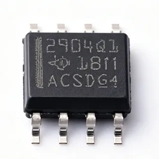
LM358ADDR - Dual 30V 700kHz Op Amp | Texas Instruments
部品番号: LM358ADDR ✓ 生産中| 数量 | 単価 | 小計 |
|---|---|---|
| 1 | $0.09 | $0.09 |
| 10 | $0.072 | $0.72 |
| 100 | $0.058 | $5.80 |
| 500 | $0.049 | $24.50 |
| 1,000 | $0.0541 | $54.10 |
LM358ADDR 概要
An operational amplifier (op amp) is a high-gain voltage amplifier with differential inputs and a single-ended output. It is a fundamental building block of analog electronics used in signal conditioning, filtering, and mathematical operations. The LM358 is a dual op amp containing two independent amplifiers in one package, offering design flexibility and space savings. It belongs to the broader category of linear integrated circuits (amplifier ICs) used across power management, sensor interfaces, and audio processing.
Key features include a common-mode input voltage range that extends to ground, enabling true single-supply operation with inputs referenced to ground. The gain-bandwidth product is 700kHz with a 0.3V/us slew rate, and maximum input offset voltage is 3mV. The operating temperature range is 0C to 70C for commercial applications. The device is RoHS compliant and lead-free.
Technically, the LM358 uses a bipolar process with a class-AB output stage for low output distortion. The PNP input pair enables the input common-mode range to include ground. The output swings close to but not rail-to-rail, a consideration for maximum-swing designs. Internal frequency compensation ensures unity-gain stability without external components.
Typical applications include transducer amplifiers, DC gain blocks, active filters, battery chargers, power supply control, and motor control loops. The dual configuration handles multiple signal paths in a compact footprint, reducing board space and component count.
When designing with the LM358ADDR, ensure input voltage does not exceed the supply rails to avoid phase reversal, decouple supply pins with 0.1uF capacitors, and account for output swing typically 1.5V from the rails. Pricing as of 2026-08-29 starts near $0.0541 at LCSC.
ドロップイン代替品: LM358ADDR — 同一パッケージでピン互換。PCBの作り直しが必要な異なるパッケージの部品は除外されています。
このシリーズのバリエーション
同一シリーズでドロップイン互換のモデル: LM358ADDR (同一形状・フットプリント) — 相違点: Amplifier Type, Gain Bandwidth Product, Package.
クイック比較ツール — 並列比較する代替部品を選択:
LM358QDRQ1
✅ ドロップイン✓ 在庫あり
$0.18 / 個
データシートを見る →LM2904DR
✅ ドロップイン ⚠️ 仕様未検証✓ 在庫あり
$0.1 / 個
データシートを見る →LM358DG
✅ ドロップイン📋 参考代替品(カタログ未掲載)
TL072CDR
✅ ドロップイン✓ 在庫あり
$0.093 / 個
データシートを見る →NJM4558D
✅ ドロップイン ⚠️ 仕様未検証📋 参考代替品(カタログ未掲載)
MC33202DR2
✅ ドロップイン ⚠️ 仕様未検証📋 参考代替品(カタログ未掲載)
LM358ADDR 最大定格&電気的特性
| Number of Channels | 2 |
| Supply Voltage Range (Single) | 3 V to 30 V |
| Supply Voltage Range (Dual) | +/-1.5 V to +/-15 V |
| Gain-Bandwidth Product | 700 kHz |
| Slew Rate | 0.3 V/us |
| Input Offset Voltage (Max) | 3 mV |
| Supply Current per Amplifier (Typ) | 500 uA |
| Input Common-Mode Range | Includes ground (single-supply) |
| 出力タイプ | Class-AB, not rail-to-rail |
| 動作温度範囲 | 0C to +70C |
| パッケージ | SOIC-8 (D) |
| 実装タイプ | Surface Mount |
| Amplifier Type | General Purpose, Bipolar |
| Unity-Gain Stability | Yes (internally compensated) |
| RoHS ステータス | Compliant |
| Lead Free | Yes |
LM358ADDR ピン構成
| ピン 1 | OUT1 — Output of amplifier 1 |
| ピン 2 | IN1- — Inverting input, amplifier 1 |
| ピン 3 | IN1+ — Non-inverting input, amplifier 1 |
| ピン 4 | GND / V- — Ground (single supply) or negative supply |
| ピン 5 | IN2+ — Non-inverting input, amplifier 2 |
| ピン 6 | IN2- — Inverting input, amplifier 2 |
| ピン 7 | OUT2 — Output of amplifier 2 |
| ピン 8 | V+ — Positive power supply, 3V to 30V |
主な用途
LM358ADDR の用途: 6 件s: Transducer and Sensor Amplifiers, Active Filter Design, Motor Control Loops, Power Supply Control and Monitoring, Battery-Powered Portable Devices, Audio Signal Processing.
Transducer and Sensor Amplifiers
The LM358ADDR's common-mode input range extending to ground makes it ideal for amplifying ground-referenced sensor signals such as thermocouples, RTD conditioners, and photodiode outputs on single 5V or 12V supplies. Its 700kHz GBW comfortably handles low-frequency sensor signals, and the dual configuration lets one package provide both gain and filter stages, halving board area versus two single op amps. Design with gain of 10-100 and keep output swings 1.5V below V+ to stay in the linear region.
おすすめ
Active Filter Design
As an internally compensated unity-gain-stable dual op amp, the LM358ADDR implements Sallen-Key and multiple-feedback active filters for audio and control signals. The 700kHz GBW limits practical corner frequencies to roughly 10-70kHz depending on Q and gain, so it suits low-pass anti-aliasing and motor-loop filters rather than RF. Both amplifiers enable 2-pole filter sections in a single SOIC-8. Use standard 0.1uF supply decoupling and account for the 3mV offset voltage in DC-coupled filter designs.
おすすめ
Motor Control Loops
In PWM motor drive systems, the LM358ADDR serves as the error amplifier in closed-loop speed and current control, comparing tachometer or shunt feedback against a setpoint. Its ground-including input range directly senses low-side shunt voltages, and the 0.3V/us slew rate is adequate for control bandwidths below 10kHz. The class-AB output drives PWM comparator inputs or RC filters. Keep the output 1.5V below the rail for linear operation, or use it as a comparator in bang-bang control schemes.
おすすめ
Power Supply Control and Monitoring
The LM358ADDR acts as a voltage monitor and error amplifier in linear regulators, battery chargers, and overvoltage protection circuits. One amplifier can regulate the output via a resistor divider from V+ while the second provides undervoltage lockout or current-limit sensing, all in one SOIC-8 operating up to 30V. Its wide 3V-30V supply range tolerates 24V industrial buses. For precision regulation better than 1%, the 3mV max offset dominates at low output voltages - add offset trimming or choose a precision amplifier for tighter tolerances.
おすすめ
Battery-Powered Portable Devices
Drawing typically 500uA per amplifier (1mA total), the LM358ADDR suits cost-sensitive battery-operated signal chains operating from single cells boosted to 3V or higher. The dual amplifiers buffer two sensor channels or implement a gain stage plus output driver in one package. Its input can sense signals at ground potential, critical for high-side-of-low-side current monitoring in portables. For stricter power budgets, modern CMOS alternatives with 10-50uA per amplifier exist, trading higher cost and offset for battery life.
おすすめ
Audio Signal Processing
The LM358ADDR provides economical gain, mixing, and active tone-control stages in consumer audio paths. Its class-AB output stage reduces crossover distortion compared to early designs, and 700kHz GBW supports full audio-bandwidth gain up to about 10 (70kHz closed-loop bandwidth). Note the output cannot swing within about 1.5V of V+, so use +/-12V or higher supplies for line-level headroom. Distortion rises when driving heavy capacitive or low-impedance loads; buffer outputs below 2k ohm loads for best performance.
おすすめ
おすすめ製品の概要
エンジニアリング参考データ: LM358ADDR — 比較、設計ガイダンス、コンプライアンス情報。
選定ガイド
代替品との比較
| パラメータ | この製品 | LM358QDRQ1 | LM2904DR | TL072CDR | MC33202DR2 |
|---|---|---|---|---|---|
| Package | SOIC-8 (D) | SOIC-8 (D) - same | SOIC-8 (D) - same | SOIC-8 (D) - same | SOIC-8 (D) - same |
| Brand | Texas Instruments | Texas Instruments | Texas Instruments | Texas Instruments | onsemi |
| Channels | 2 | 2 | 2 | 2 | 2 |
| Gain-Bandwidth Product | 700 kHz | 700 kHz | 700 kHz | 3 MHz | 2.2 MHz |
| Supply Voltage Range | 3 V to 30 V | 3 V to 30 V | 3 V to 26 V | 6.5 V (min) dual-supply | 2.2 V to 12 V |
| Operating Temperature | 0C to +70C | -40C to +125C | -40C to +125C | 0C to +70C | -40C to +105C |
| Automotive Grade | No | Yes (AEC-Q100) | Yes (AEC-Q100 eligible family) | No | No |
| Rail-to-Rail Output | No (~1.5V from rail) | No | No | No | Yes |
主な差別化要因
- Ground-sensing input for true single-supply operation (vs TL072CDR)
- Lowest cost general-purpose dual op amp (vs MC33202DR2)
- Automotive drop-in available (vs LM358QDRQ1)
設計ノート
Decouple the V+ pin (pin 8) with a 0.1uF ceramic capacitor placed within 5mm of the pin, plus a 10uF bulk capacitor per board section. The LM358 class-AB output draws load-dependent current spikes that can couple into nearby precision circuitry through shared supply impedance. On single supplies above 15V, verify total dissipation stays within SOIC-8 thermal limits (about 625mW at 25C ambient per TI LM358 datasheet).
Do not drive the inputs above V+; the LM358 can exhibit phase reversal when input common-mode exceeds the specified range, latching the output high. Also remember the output saturates about 1.5V below V+ (and about 5-20mV above ground), so gain-stage headroom calculations must use the reduced swing or the design will clip unexpectedly near the positive rail.
Keep input traces short and guard the high-impedance inverting node to limit leakage-induced offset; the 3mV maximum offset already dominates accuracy in DC-coupled gains above 10. For capacitive loads greater than about 50pF, add an isolation resistor (50-100 ohm) in series with the output to preserve phase margin and prevent ringing, per the TI LM358 application section.
SOIC-8 theta_JA is approximately 100-130 C/W on a typical 4-layer board; at 30V supply driving a heavy load, junction temperature can rise quickly. Estimate Pd = (V+ - VOUT) * ILOAD per amplifier and keep total under 400mW in 70C ambients for margin. The 0C to +70C rating of the commercial LM358ADDR makes it unsuitable for automotive under-hood use - select LM358QDRQ1 instead.
コンプライアンス情報
RoHS compliant and lead-free per TI product data. Commercial-grade 0C to +70C; not AEC-Q100 qualified - use LM358QDRQ1 for automotive.