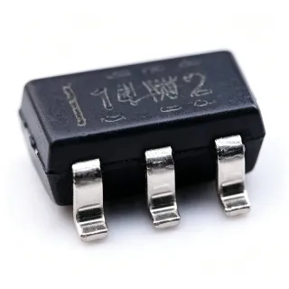
LMV321IDBVR - 1-MHz RRO Op Amp Single 5.5V | Texas Instruments
部品番号: LMV321IDBVR ✓ 生産中| 数量 | 単価 | 小計 |
|---|---|---|
| 1 | $0.34 | $0.34 |
| 10 | $0.28 | $2.80 |
| 100 | $0.19 | $19.00 |
| 500 | $0.16 | $80.00 |
| 1,000 | $0.14 | $140.00 |
| 3,000 | $0.12 | $360.00 |
LMV321IDBVR 概要
A rail-to-rail output (RRO) op amp is a linear amplifier whose output voltage can swing to within tens of millivolts of either supply rail, maximizing dynamic range in low-voltage single-supply systems. Compared with general-purpose amplifiers that lose 1 V to 2 V of headroom on each side, an RRO part lets the designer use the full ADC input range on a 3.3 V or 5 V rail. The LMV321 belongs to the broader family of CMOS operational amplifiers, a category of analog ICs that trades the lower noise of bipolar parts for very low quiescent current and single-supply operation.
Key features include 1 MHz gain bandwidth product, 130 µA typical quiescent current, no output phase reversal, low crossover distortion, and an industry-standard 5-pin SOT-23 footprint. An internal ESD clamp and EMI filtering are characteristics of the larger LMV321A family; the original LMV321 line is recommended for cost-sensitive designs where these features are not required. The device is unity-gain stable and drives 2 kΩ loads comfortably at 5 V.
The LMV321 is built on a CMOS process with a differential input pair and a rail-to-rail class-AB output stage, which keeps crossover distortion low compared to single-ended class-A CMOS outputs. The PSRR is specified at 50 dB at 1 kHz, and the input common-mode range extends from the negative rail to within 1.2 V of the positive rail — adequate for single-supply sensor buffers and instrumentation front-ends.
Typical applications include single-supply sensor signal conditioning, current-sensing shunts in portable battery packs, low-side current monitors, headphone line drivers, and 5 V active filters. The part is widely used as a buffer/amplifier stage between photodiodes, thermistors, or strain gauges and downstream ADCs in IoT nodes.
When designing with this device, place a 1 nF to 10 nF decoupling capacitor within 2 mm of the VCC pin and keep input trace lengths short to limit leakage-induced offsets. For driving heavy loads or large capacitive loads, add a 50 Ω to 100 Ω series resistor at the output to prevent oscillation.
This page synthesizes distributor pricing, drop-in same-footprint alternatives, and practical design notes not found in the manufacturer datasheet.
ドロップイン代替品: LMV321IDBVR — 同一パッケージでピン互換。PCBの作り直しが必要な異なるパッケージの部品は除外されています。
このシリーズのバリエーション
同一シリーズでドロップイン互換のモデル: LMV321IDBVR (同一形状・フットプリント) — 相違点: Number of Channels, Operating Temperature Range, Output Type, Input Type, Input Voltage Noise Density.
クイック比較ツール — 並列比較する代替部品を選択:
LMV321AIDBVR
✅ ドロップイン📋 参考代替品(カタログ未掲載)
TLV3201AIDBVR
✅ ドロップイン📋 参考代替品(カタログ未掲載)
TLV9061IDBVR
✅ ドロップイン📋 参考代替品(カタログ未掲載)
TLV9041IDBVR
✅ ドロップイン📋 参考代替品(カタログ未掲載)
TSV321IDBVR
✅ ドロップイン📋 参考代替品(カタログ未掲載)
LMV321SN3T1G
✅ ドロップイン📋 参考代替品(カタログ未掲載)
TP321-TR
✅ ドロップイン📋 参考代替品(カタログ未掲載)
LMV321IDBVR 最大定格&電気的特性
| Number of Channels | 1 (Single) |
| 出力タイプ | Rail-to-Rail |
| Gain Bandwidth Product (GBP) | 1 MHz |
| Supply Voltage (Single, 5V characterized) | 2.7 V to 5.5 V |
| Quiescent Current (typ) | 130 µA |
| Power Supply Rejection Ratio (PSRR) | 50 dB at 1 kHz (per family datasheet summary) |
| 動作温度範囲 | -40 °C to +125 °C |
| パッケージ | SOT-23-5 (DBV) |
| 実装タイプ | Surface Mount |
| MSLレベル | 1 (unlimited floor life, per JEDEC J-STD-020) |
| RoHS ステータス | Compliant |
| Lead-Free Finish | Yes (NiPdAu) |
LMV321IDBVR ピン構成
| ピン 1 | OUT — Amplifier output (rail-to-rail) |
| ピン 2 | VCC- / IN- — Negative supply / inverting input (per LMV321 DBV pinout) |
| ピン 3 | IN+ — Non-inverting input |
| ピン 4 | VCC — Positive supply (2.7 V to 5.5 V) |
| ピン 5 | NC — Not connected (per datasheet pinout) |
主な用途
LMV321IDBVR の用途: 6 件s: Battery-Powered Sensor Signal Conditioning, Low-Side Current Sensing Amplifier, Headphone / Audio Line Driver, Photodiode Transimpedance Amplifier, Active Filter for ADC Anti-Aliasing, Industrial 4-20 mA Current Loop Transmitter.
Battery-Powered Sensor Signal Conditioning
The LMV321IDBVR is widely deployed as the front-end amplifier for low-frequency analog sensors (thermistor, strain gauge, pH probe, gas sensor) in coin-cell and 2 x AA battery products. Its 130 µA typical quiescent current adds negligible load to the cell while still delivering 1 MHz GBP — enough to buffer high-impedance sensor outputs without 1/f noise overwhelming the signal. The rail-to-rail output lets the next-stage ADC use the full 0 V to VCC input range, doubling usable dynamic range versus a non-RRO part on a 3.3 V rail. In a typical design, the LMV321 sits between a 10 kΩ Wheatstone bridge and a 12-bit SAR ADC running at 100 kSPS, with a 10 nF decoupling cap within 2 mm of the VCC pin.
おすすめ
Low-Side Current Sensing Amplifier
For battery management and motor-drive current monitoring, the LMV321IDBVR is used as a differential amplifier across a 10 mΩ to 100 mΩ shunt resistor. Its input common-mode range to the negative rail is essential because the shunt sits in series with the load return, which can be near ground or below ground during inductance ringing. The 1 MHz GBP introduces only ~5 µs of additional delay at 50 kHz PWM frequencies — adequate for sub-kHz current loops. Designers bias the non-inverting input to VCC/2 with a resistor divider to keep the output within the rail, and add a 50 Ω series output resistor if the load is capacitive.
おすすめ
Headphone / Audio Line Driver
Consumer headphone amplifiers and line-level audio outputs frequently use the LMV321IDBVR as a unity-gain buffer driving 16 Ω to 32 Ω earphones from a low-voltage DAC. Its rail-to-rail output swing maximizes the audio dynamic range on a 3.3 V or 5 V rail, while 1 MHz GBP comfortably covers the 20 Hz to 20 kHz audio band with low distortion. The 130 µA Iq keeps total idle current in the single-digit mW region, important for battery-powered Bluetooth headphones. A typical circuit adds an AC-coupling capacitor in series with the output and a 10 kΩ load to ground, with the part operating from VCC = 3.3 V.
おすすめ
Photodiode Transimpedance Amplifier
A single LMV321IDBVR can function as a low-cost transimpedance front-end for visible-light or IR photodiodes in smoke detectors, heart-rate monitors, or proximity sensors. The 1 MHz GBP and low input bias current (sub-pA with CMOS inputs) support feedback resistors up to ~1 MΩ without instability, giving sensitivities in the µA/nW range. Because the photodiode is biased near ground and the op-amp output sits near VCC/2, the rail-to-rail output stage keeps the diode in its linear region even on 3.3 V supplies. A 10 pF feedback capacitor in parallel with Rf prevents peaking, and the 5-pin SOT-23 footprint keeps the BOM cost below $0.20.
おすすめ
Active Filter for ADC Anti-Aliasing
The LMV321IDBVR works well as a Sallen-Key or multiple-feedback active low-pass filter for 3rd-order, 4th-order anti-aliasing stages ahead of sigma-delta ADCs in instrumentation and metering. With 1 MHz GBP, designers can realize filter corner frequencies up to ~50 kHz while maintaining at least 20 dB of gain margin at the unity-gain crossover. The rail-to-rail output stage allows the filter output to track the ADC's common-mode input, simplifying single-supply designs. A 4th-order Butterworth with fc = 10 kHz is a common recipe; placing a 10 nF to 100 nF capacitor across the feedback resistor tames peaking at the resonant frequency.
おすすめ
Industrial 4-20 mA Current Loop Transmitter
On the transmitter side of an industrial 4-20 mA current loop, the LMV321IDBVR can be used as the error amplifier inside the V-to-I converter that drives the loop. Its ability to operate from a single 5 V rail and stay within 2.7 V to 5.5 V across wide temperature ranges suits 24 V industrial loops after the local regulator drops to 5 V. The 130 µA Iq keeps the loop itself well above 4 mA at zero signal. A typical circuit uses the LMV321 with a 250 Ω sense resistor and a 2N3904 pass transistor, creating a stable 4 mA to 20 mA loop from a 0 V to 4 V DAC output.
おすすめ
おすすめ製品の概要
エンジニアリング参考データ: LMV321IDBVR — 比較、設計ガイダンス、コンプライアンス情報。
選定ガイド
代替品との比較
| パラメータ | この製品 | LMV321AIDBVR | TLV3201AIDBVR | TLV9061IDBVR | TSV321IDBVR | LMV321SN3T1G | TP321-TR |
|---|---|---|---|---|---|---|---|
| Brand | Texas Instruments | Texas Instruments | Texas Instruments | Texas Instruments | STMicroelectronics | onsemi | 3PEAK |
| Package | SOT-23-5 (DBV) | SOT-23-5 (DBV) — same | SOT-23-5 (DBV) — same | SOT-23-5 (DBV) — same | SOT-23-5 (DBV) — same | SOT-23-5 (DBV) — same | SOT-23-5 (DBV) — same |
| Channels | 1 (Single) | 1 (Single) | 1 (Single, comparator) | 1 (Single) | 1 (Single) | 1 (Single) | 1 (Single) |
| Supply Voltage Range | 2.7 V to 5.5 V | 2.7 V to 5.5 V | 2.7 V to 5.5 V | 1.8 V to 5.5 V (wider) | 2.5 V to 5.5 V | 2.7 V to 5.5 V | 2.5 V to 5.5 V |
| Gain Bandwidth Product | 1 MHz | 1 MHz | N/A (comparator; prop delay 40 ns) | 10 MHz | 1.4 MHz | 1 MHz | 1 MHz |
| Quiescent Current (typ) | 130 µA | 130 µA | 50 µA | 538 µA | 500 µA | 130 µA | 150 µA |
| Output Type | Rail-to-Rail Output | Rail-to-Rail Output | Open-Drain / Push-Pull comparator output | Rail-to-Rail I/O | Rail-to-Rail Output | Rail-to-Rail Output | Rail-to-Rail Output |
| Operating Temperature | -40 °C to +125 °C | -40 °C to +125 °C | -40 °C to +125 °C | -40 °C to +125 °C | -40 °C to +125 °C | -40 °C to +85 °C (commercial) | -40 °C to +125 °C |
| Approx. Unit Price (qty 1000) | $0.14 | $0.18 (est.) | $0.28 (est.) | $0.30 (est.) | $0.22 (est.) | $0.16 (est.) | $0.05 (est., China-domestic) |
主な差別化要因
- Industry-benchmark cost / availability in SOT-23-5 (vs TLV9061IDBVR)
- Mature, broadly second-sourced design (vs TLV9041IDBVR)
- Higher bandwidth vs lower-Iq competitor (vs TSV321IDBVR)
設計ノート
Decouple VCC with a 0.1 µF ceramic capacitor placed within 2 mm of the supply pin, in parallel with a 1 µF to 10 µF bulk capacitor at the regulator output. The LMV321's 130 µA quiescent current is small enough that supply-line noise from a switching regulator can couple into the output — add an RC pi-filter (10 Ω + 10 µF) on the VCC rail if the part follows a noisy DC-DC converter. Estimated: power dissipation at 5 V is ~0.65 mW, well within SOT-23-5 thermal limits.
Route input traces away from noisy digital or switching signals; keep trace impedance below 100 Ω by using a ground plane on the input layer. For photodiode TIA applications, minimize the loop area of the feedback resistor and capacitor to limit stray capacitance — every extra pF of feedback capacitance reduces phase margin by roughly 1.5 ° per pF at the unity-gain crossover, and instability appears above ~5 pF with a 1 MΩ Rf.
The CMOS input stage has very low bias current but is sensitive to ESD; if the input will be exposed to user-accessible connectors, add a TVS diode and a 10 kΩ to 100 kΩ series resistor. The LMV321A variant integrates internal RFI/EMI filtering and 4 kV HBM ESD — preferred for industrial or human-interface designs. Do not drive the input above (VCC + 0.3 V) or below (VCC- − 0.3 V); use a clamping circuit if the input can exceed the rails during fault conditions.
The LMV321DBV and the LMV321M5 share the same SOT-23-5 outline but have different pin assignments — substituting one for the other without rerouting the PCB will short VCC to ground. Always check pin 1 orientation (the dot or tab mark) against the schematic before assembly. Estimating from the family datasheet: the LMV321 does not include an enable/shutdown pin; if low-Iq standby is required, choose TLV9041 (nanoPower) or add an external MOSFET load switch.
コンプライアンス情報
RoHS and lead-free status confirmed on TI product page and DigiKey listing. REACH compliance per TI product environmental information. AEC-Q100 not applicable — op amp not automotive-qualified by default; use TLV9061-Q1 for automotive designs.