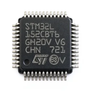
LPC1313FBD48/01 - 72MHz Cortex-M3 MCU | NXP | Embedded
部品番号: LPC1313FBD48/01 ✗ 生産終了LPC1313FBD48/01 概要
A microcontroller is a programmable system-on-chip that combines a processor core, memory, peripherals, and communication interfaces on one semiconductor device. The LPC1313FBD48/01 belongs to the MCU, embedded processor, and power-management-IC hierarchy. Its Cortex-M3 architecture provides a compact platform for control-oriented products, while its integrated interfaces allow the device to operate without several discrete interface components.
Key features include operation at up to 72 MHz, as much as 32 kB of embedded flash, and as much as 8 kB of SRAM. The peripheral set includes one Fast-mode Plus I2C interface, one UART, four general-purpose counter or timer blocks, and as many as 40 I/O ports. The 2 V to 3.6 V operating-voltage range supports low-voltage embedded systems, while the 48-pin LQFP package exposes the mixed-signal and digital resources through a conventional leaded footprint.
The LPC1313 family combines a deterministic Arm Cortex-M3 processor core with an integrated peripheral set intended for cost-sensitive embedded control. Flash memory supports in-system firmware storage, and the SRAM provides working memory for control code, interrupt handling, and peripheral data. The I2C and UART interfaces support connection to external sensors, EEPROMs, transceivers, and host controllers. Additional GPIO permits digital inputs, outputs, interrupt sources, and basic control signaling to be consolidated on the same device.
Typical applications include industrial sensor nodes, building and access-control equipment, consumer accessories, low-power data collectors, embedded USB peripherals, and compact control boards. A 72 MHz Cortex-M3 can manage multiple interrupt-driven peripherals, protocol handling, and application logic without requiring a higher-complexity processor. For designs requiring several independent timers, sensor interfaces, or communications channels, the integrated resources reduce board area and reduce the number of external devices.
The principal design consideration is the 2 V to 3.6 V supply range. The power architecture, regulator design, decoupling, and I/O voltage levels must therefore be coordinated so that every external signal remains within the device's electrical limits. Because the family has a published end-of-life notice, engineers should also confirm the exact orderable suffix, longevity requirements, and migration path before beginning a long-life production design.
This product page consolidates the official NXP device description, package and memory characteristics, lifecycle information, interface details, and same-family replacement guidance. It also adds application-oriented selection guidance and practical design notes to help engineers evaluate the LPC1313FBD48/01 beyond basic catalogue information.
ドロップイン代替品: LPC1313FBD48/01 — 同一パッケージでピン互換。PCBの作り直しが必要な異なるパッケージの部品は除外されています。
このシリーズのバリエーション
同一シリーズでドロップイン互換のモデル: LPC1313FBD48/01 (同一形状・フットプリント) — 相違点: Package, Flash Memory.
LPC1343FBD48,151
✅ ドロップイン価格はお問い合わせください
データシートを見る →LPC1345FBD48,151
✅ ドロップイン価格はお問い合わせください
データシートを見る →LPC1313FBD48/01 最大定格&電気的特性
| Product Type | 32-bit ARM Cortex-M3 microcontroller |
| CPU Core | Arm Cortex-M3 |
| Maximum CPU Frequency | 72 MHz |
| Flash Memory | Up to 32 kB |
| Data Memory | Up to 8 kB |
| Program Memory Type | Flash |
| 動作電源電圧 | 2 V to 3.6 V |
| I2C Interface | 1 Fast-mode Plus (Fm+) I2C interface |
| UART Interface | 1 UART |
| General-Purpose Timer Count | 4 |
| I/O Port Count | 40 |
| パッケージ | 48-pin LQFP, 7 mm x 7 mm |
| Package Height | 1.40 mm |
| 実装タイプ | Surface mount |
LPC1313FBD48/01 1.40 mm ピン配置ガイド
LPC1313FBD48/01 (1.40 mm パッケージ) のピン配置。 このデジタルICには、GPIO、通信インターフェース (UART、SPI、I2C)、および電源ピンが含まれています。代替ピン機能と設定オプションについては、メーカーのデータシートを参照してください。組み込みシステム設計とPCBレイアウトに不可欠です。

詳細なピン配置データはありません: LPC1313FBD48/01.
詳細は データシート をご参照ください。
主な用途
LPC1313FBD48/01 の用途: 6 件s: Industrial Sensor and Control Nodes, USB Connectivity and Peripherals, Building Access and Security Equipment, Consumer Data Collection and HMI, Battery-Powered Monitoring Equipment, Communication Interface Modules.
Industrial Sensor and Control Nodes
The LPC1313FBD48/01 fits compact industrial sensor nodes that need deterministic control, several timing resources, and low-voltage operation. Its Arm Cortex-M3 core can run up to 72 MHz, while four general-purpose timers support periodic sampling, timeout handling, capture, or compare functions. The Fast-mode Plus I2C interface can connect compatible sensors and EEPROMs, and the UART provides a simple path to an upstream controller. With up to 32 kB of flash and 8 kB of SRAM, the MCU can hold protocol handlers, filtering logic, and control code without requiring external memory. The 2 V to 3.6 V range suits 3.3 V industrial equipment, provided transient protection and grounding are designed for the installation environment.
おすすめ
USB Connectivity and Peripherals
The LPC1313FBD48/01 is applicable to USB-enabled embedded accessories and control peripherals where a compact Cortex-M3 platform is needed. The manufacturer describes the LPC1313 family as a USB device capable of combining up to 32 kB of flash and 8 kB of SRAM with communication peripherals. That combination is useful for implementing USB enumeration, descriptor handling, control commands, and application-specific functions in one device. Its 72 MHz maximum CPU frequency provides headroom for protocol processing and background tasks, while I2C and UART support sensor or host-side expansion. PCB implementation must follow the manufacturer's USB and power guidance, including correct signal routing, decoupling, and the device-specific pin assignments.
おすすめ
Building Access and Security Equipment
The LPC1313FBD48/01 supports access-control readers, keypads, door interfaces, and compact security modules that coordinate several discrete functions. Its 40 I/O ports provide ample digital connections for indicators, buttons, lock-control signals, tamper inputs, and status lines, while four timers can manage debounce, pulse timing, access intervals, or actuator control. The Cortex-M3 core operates up to 72 MHz, allowing the firmware to combine credential processing, event logging, communications, and real-time control. Fast-mode Plus I2C is suitable for compatible secure elements or configuration memories, and the UART supports system-level diagnostics. As the LPC13xx family has an end-of-life notice, new security designs should include a planned migration path and confirm suffix-specific availability.
おすすめ
Consumer Data Collection and HMI
The LPC1313FBD48/01 can serve as the controller in compact consumer interfaces, data loggers, and appliance subcontrollers where local logic must coordinate a display, keypad, sensor, or communications module. Its 72 MHz Cortex-M3 performance is suitable for responsive menu handling, data conditioning, and interrupt-driven peripheral management. The Fast-mode Plus I2C interface supports compatible sensors, display drivers, or configuration devices, while the UART provides a straightforward link to a host or service module. Forty I/O pins allow status LEDs, buttons, and discrete controls to remain close to the MCU. The 2 V to 3.6 V supply range simplifies integration into 3.3 V consumer electronics, although power consumption should be assessed across active and low-power operating modes.
おすすめ
Battery-Powered Monitoring Equipment
The LPC1313FBD48/01 is relevant to battery-powered monitoring and metering equipment because it consolidates processing, flash, SRAM, timers, and serial interfaces within a single low-voltage device. At 72 MHz it can support responsive measurement control and data processing, while its 32 kB flash capacity accommodates compact firmware and calibration information. I2C can connect suitable sensors or memory, UART can provide diagnostics or a host link, and the timers can establish accurate sampling intervals. The 2 V minimum operating voltage can assist battery-energy utilization, but the complete system budget must include sensor load, regulator quiescent current, and communications activity. Firmware should use the device's low-power operating modes when the application permits intermittent operation.
おすすめ
Communication Interface Modules
The LPC1313FBD48/01 is suitable for protocol adapters and communication modules that need a fast control core plus standardized serial interfaces. Its Cortex-M3 architecture executes at up to 72 MHz, allowing software handling of framing, checksums, state machines, and diagnostic commands. One Fast-mode Plus I2C interface can operate alongside the UART, allowing a module to bridge or supervise sensors, memories, transceivers, and host connections without a separate logic device. Forty GPIO lines add flexibility for modem-control signals, status indicators, configuration straps, and interrupts. The 48-LQFP package also provides a conventional assembly option for industrial or appliance equipment, subject to the manufacturer's land-pattern, solder, and decoupling requirements.
おすすめ
おすすめ製品の概要
エンジニアリング参考データ: LPC1313FBD48/01 — 比較、設計ガイダンス、コンプライアンス情報。
選定ガイド
代替品との比較
| パラメータ | この製品 | LPC1343FBD48 | LPC1345FBD48 |
|---|---|---|---|
| Package | 48-LQFP (7x7) | 48-LQFP (7x7) | 48-LQFP (7x7) |
| Brand | NXP Semiconductors | NXP Semiconductors | NXP Semiconductors |
| CPU Core | Arm Cortex-M3 | Arm Cortex-M3 | Arm Cortex-M3 |
主な差別化要因
- Direct match to an established 72 MHz Cortex-M3 embedded-control design (vs LPC1343FBD48)
- Defined 48-pin LQFP migration path within the LPC13xx family (vs LPC1345FBD48)
- Documented integration of 40 I/O ports and four general-purpose timers (vs LPC1343FBD48)
設計ノート
Design the supply rail for the stated 2 V to 3.6 V operating range and place the required decoupling capacitors at the device power pins with the shortest practical return paths. Use the pin-description table in the manufacturer datasheet to identify all supply and ground connections. Confirm regulator startup, load-transient response, and every attached peripheral's voltage level; do not assume that a nominal 3.3 V rail is compatible with every external interface.
Use the manufacturer's 48-pin LQFP land pattern and follow its assembly guidance for pad geometry, solder mask, paste, and the board outline around the 7 mm by 7 mm package. Preserve access for inspection and rework, and maintain adequate copper and thermal pathways for the device's normal dissipation. Because migration candidates can change peripheral functions, keep the PCB design documented by signal rather than by generic GPIO numbering.
Route sensitive analogue or communication signals away from switching nodes and high-current return paths, while keeping the Cortex-M3 supply, ground, and decoupling network compact. I2C and USB-related routing must follow the manufacturer's electrical and layout guidance, including appropriate trace geometry and return-path continuity. If an external transceiver is used, isolate its high-energy interface section from the MCU and its reference components.
Do not treat a related LPC13xx model as a drop-in part solely because it has the same family name and 48-pin LQFP outline. Compare the complete pin tables, clock requirements, peripheral multiplexing, USB behaviour, startup configuration, and software-driver support for LPC1343FBD48 or LPC1345FBD48. A successful hardware fit does not by itself establish software or functional compatibility.
コンプライアンス情報
The available product information does not provide a complete suffix-specific RoHS, REACH, AEC-Q100, lead-free, halogen-free, or conflict-minerals declaration. Obtain the current material and compliance documents from NXP for the exact orderable suffix.