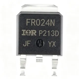
SQD50P08-28 - 80V P-Channel 48A TrenchFET MOSFET | Vishay
部品番号: SQD50P08-28 ✓ 生産中| 数量 | 単価 | 小計 |
|---|---|---|
| 1 | $1.85 | $1.85 |
| 10 | $1.65 | $16.50 |
| 100 | $1.42 | $142.00 |
| 500 | $1.18 | $590.00 |
| 1,000 | $0.95 | $950.00 |
| 3,000 | $0.82 | $2,460.00 |
SQD50P08-28 概要
What is a P-channel MOSFET? A P-channel MOSFET is a type of field-effect transistor in which the channel is formed by holes flowing from source to drain when a negative gate-to-source voltage is applied. As a member of the broader MOSFET hypernym hierarchy (P-channel MOSFET -> MOSFET -> FET -> power transistor -> discrete semiconductor), it is commonly used for high-side switching because it can be turned on by pulling the gate toward ground. The SQD50P08-28 specifically uses Vishay's TrenchFET technology, which reduces RDS(on) by etching vertical trenches into the silicon, dramatically lowering conduction losses versus planar MOSFETs.
Key specifications include a maximum on-resistance of 28 mΩ at VGS = -10 V, a maximum gate threshold of -2.5 V (typical), and an operating junction temperature up to 175 °C. The TO-252AA package provides a low-profile surface-mount form factor suitable for automated PCB assembly while maintaining thermal performance for power dissipation. The device is halogen-free per Vishay's documentation and is supplied in tape-and-reel packaging for high-volume manufacturing.
Typical applications include automotive load switching such as LED lighting drivers, HVAC blower motor control, power seat modules, and body electronics where high-side switches are preferred for fail-safe behavior. The P-channel topology eliminates the need for a charge pump or bootstrap circuit that would be required for an N-channel high-side switch, simplifying gate drive design. The 80 V rating also provides ample headroom for 12 V and 24 V automotive bus transients including load-dump pulses.
Design considerations include ensuring the gate drive circuit can pull the gate to within -10 V of source for full enhancement, and providing adequate PCB copper area for thermal dissipation at high currents. Because P-channel devices have higher RDS(on) per unit silicon area than comparable N-channel parts, the SQD50P08-28 is best suited for switching applications rather than continuous linear operation.
ドロップイン代替品: SQD50P08-28 — 同一パッケージでピン互換。PCBの作り直しが必要な異なるパッケージの部品は除外されています。
クイック比較ツール — 並列比較する代替部品を選択:
SQD50P08-28_GE3
✅ ドロップイン📋 参考代替品(カタログ未掲載)
SQD50P08-28_NE3
✅ ドロップイン📋 参考代替品(カタログ未掲載)
SQD50P08-25L
✅ ドロップイン📋 参考代替品(カタログ未掲載)
SQD50P08-28 最大定格&電気的特性
| Manufacturer | Vishay Siliconix |
| Part Family | TrenchFET Power MOSFET |
| FET Type | P-Channel |
| Configuration | Single |
| Drain-to-Source Voltage (VDS) | -80 V |
| Continuous Drain Current (ID) at TC | -48 A |
| Power Dissipation (PD) at TC | 136 W |
| On-Resistance RDS(on) at VGS = -10 V | 28 mΩ (max) |
| 動作接合温度 | -55 °C to +175 °C |
| パッケージ | TO-252AA (DPAK) |
| 実装タイプ | Surface Mount |
| Automotive Qualification | AEC-Q101 Qualified |
| Test Coverage | 100% Rg tested, 100% UIS tested |
| ハロゲンフリー | Yes |
| RoHS ステータス | Compliant |
SQD50P08-28 ピン構成
| ピン 1 | GATE — Gate control input (drive to near source potential to turn on P-channel) |
| ピン 2 | DRAIN — Drain (also connected to metal tab/back thermal pad) |
| ピン 3 | SOURCE — Source (typically connected to higher-potential supply rail for high-side switching) |
安全動作領域 (DC, TC=25°C)
主な用途
SQD50P08-28 の用途: 6 件s: Automotive LED Lighting Drivers, HVAC Blower Motor Control, Power Seat and Window Lift Modules, Battery Management System (BMS) Protection, Body Control Modules and Load Switches, Industrial 24V Bus Switching.
Automotive LED Lighting Drivers
The SQD50P08-28 serves as a high-side switch in automotive LED headlight and tail-light modules, where its P-channel topology eliminates the need for a charge pump. With -80 V VDS, -48 A ID, and 28 mΩ RDS(on) at VGS = -10 V, it efficiently handles the 12 V automotive bus while providing ample headroom for load-dump transients up to 35 V. AEC-Q101 qualification and 100% UIS testing ensure long-term reliability under the thermal and vibration stresses of under-hood and exterior lighting installations. Pair with a Vishay SQ7414 gate driver for sequenced turn-on and fault detection.
おすすめ
HVAC Blower Motor Control
In HVAC blower motor control modules, the SQD50P08-28 provides PWM-switched high-side control of fractional-horseprint blower motors drawing up to 30 A continuous. Its 136 W power dissipation rating at TC and TO-252AA package enable compact PCB integration with sufficient thermal margin. The 80 V rating protects against back-EMF transients when switching inductive loads, while AEC-Q101 qualification ensures operation across -40 °C to +125 °C ambient under-hood conditions. 100% UIS testing confirms robustness against unclamped motor kickback events common in PWM-driven inductive loads.
おすすめ
Power Seat and Window Lift Modules
The SQD50P08-28 is well-suited for power seat adjustment and window lift motor reverse-polarity protection circuits where bidirectional current blocking is required. Its P-channel configuration in a high-side H-bridge half-bridge position provides fail-safe default-off behavior when gate drive is removed, a critical safety feature in automotive body electronics. With 28 mΩ RDS(on) at -10 V VGS and 48 A continuous current capability, it handles the stall currents of small DC gear motors used in seat tracks and window regulators while dissipating minimal heat in a compact TO-252AA footprint.
おすすめ
Battery Management System (BMS) Protection
In 12 V automotive battery management systems, the SQD50P08-28 functions as a reverse-polarity protection FET or load disconnect switch on the high side of the battery rail. Its -80 V VDS rating exceeds the maximum expected battery voltage under all conditions including jump-start from a 24 V truck, while its 48 A continuous rating covers typical accessory loads. The P-channel topology ensures the load remains disconnected if gate drive fails, providing inherent fail-safe behavior critical for battery protection circuits where unintended discharge could leave a vehicle stranded.
おすすめ
Body Control Modules and Load Switches
Distributed body control modules use the SQD50P08-28 to switch various resistive and inductive loads including door lock actuators, mirror heaters, and wiper motors. Each module typically contains multiple high-side switches, and the TO-252AA package with 28 mΩ RDS(on) provides an excellent balance of footprint efficiency and thermal performance. AEC-Q101 qualification with 100% Rg testing ensures consistent switching characteristics across production lots, critical for modules that must meet tight EMI/EMC emissions limits set by automotive OEMs worldwide.
おすすめ
Industrial 24V Bus Switching
Beyond automotive, the SQD50P08-28 serves as a robust high-side switch in industrial 24 V control systems including PLCs, sensor power distribution, and solenoid drivers. Its 80 V rating provides >3x safety margin over nominal 24 V rails with tolerance for industrial supply transients, while the 48 A continuous rating handles most industrial load switching requirements. The TO-252AA surface-mount package enables high-density PCB designs, and although designed for automotive, the device's extended temperature range of -55 °C to +175 °C makes it suitable for industrial environments without automotive-grade cost premiums when AEC-Q101 is not required.
おすすめ
おすすめ製品の概要
エンジニアリング参考データ: SQD50P08-28 — 比較、設計ガイダンス、コンプライアンス情報。
選定ガイド
代替品との比較
| パラメータ | この製品 | SQD50P08-28_GE3 | SQD50P08-28_NE3 | SQD50P08-25L |
|---|---|---|---|---|
| Brand | Vishay Siliconix | Vishay Siliconix | Vishay Siliconix | Vishay Siliconix |
| Package | TO-252AA (DPAK) | TO-252AA (DPAK) - same | TO-252AA (DPAK) - same | TO-252AA (DPAK) - same |
| Drain-to-Source Voltage (VDS) | -80 V | -80 V | -80 V | -80 V |
| Continuous Drain Current (ID at TC) | -48 A | -48 A | -48 A | -48 A |
| RDS(on) max at VGS=-10V | 28 mΩ | 28 mΩ | 28 mΩ | 25 mΩ (lower) |
| Power Dissipation (PD at TC) | 136 W | 136 W | 136 W | 136 W |
| Automotive Qualification | AEC-Q101 | AEC-Q101 | AEC-Q101 | AEC-Q101 |
| Halogen-Free | Variant dependent | Yes (GE3 suffix) | No (NE3 suffix) | Variant dependent |
主な差別化要因
- Halogen-free construction available with GE3 suffix (vs SQD50P08-28_NE3)
- Lower on-resistance option available within same family (vs SQD50P08-25L)
- Same die across multiple orderable part numbers (vs SQD50P08-28_GE3 / SQD50P08-28_NE3)
設計ノート
Estimated: at 48 A continuous drain current with 28 mΩ RDS(on), conduction loss is approximately I² × R = 48² × 0.028 = 64.5 W. In the TO-252AA package with the thermal pad soldered to the PCB, ensure at least 1 square inch of 2 oz copper area on the drain tab to keep junction temperature rise within safe limits. Without adequate copper, the device will desolder the tab or trigger thermal shutdown at high ambient temperatures. For continuous operation above 30 A, forced air cooling or a heatsink attached to the drain tab is recommended.
The TO-252AA drain tab is electrically connected to pin 2 (DRAIN). For high-side switching applications, this means the heatsink or PCB copper spreader is at drain potential, not ground. Isolate the drain copper area from low-voltage control circuitry and use thermal interface materials rated for the drain voltage if attaching external heatsinks. Place the gate drive traces away from the drain copper to minimize capacitive coupling that could cause unintended turn-on during drain voltage transients.
Do not assume VGS(th) from one Vishay P-channel datasheet applies to all variants - VGS(th) for the SQD50P08-28 should be verified in the specific datasheet document 63215 before designing the gate drive circuit. Also note that P-channel MOSFETs have higher RDS(on) than equivalently sized N-channel parts, so the SQD50P08-28 should not be used as a drop-in for an N-channel circuit. Ensure gate drive pulls to within -10 V of source for full enhancement; weak gate drive at -4.5 V can result in 2-3x higher conduction loss.
コンプライアンス情報
AEC-Q101 (automotive) qualified per Vishay product page. GE3 suffix indicates halogen-free; NE3 suffix indicates standard RoHS-compliant non-halogen-free. RoHS and REACH compliance confirmed across all variants per Vishay documentation.