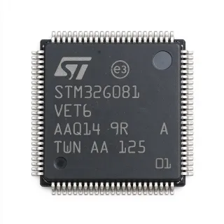
STM32F105VBT6 - 72MHz Cortex-M3 MCU | STMicroelectronics
部品番号: STM32F105VBT6 ✓ 生産中STM32F105VBT6 概要
A microcontroller is a semiconductor system that integrates a processor core, memory, peripherals, and I/O into one compact device. Within the product hierarchy, the STM32F105VBT6 is an ARM Cortex-M3 MCU, part of the STM32 product family and the STM32F1 series, and ultimately a category of embedded processor and semiconductor. Its combination of 72 MHz processing, 128 KB Flash, and extensive pin connectivity makes it suitable for systems that need deterministic control alongside multiple communication and general-purpose I/O functions.
The main technical features of this device include its 72 MHz ARM Cortex-M3 core, 128 KB Flash, 32-bit processing architecture, and 100-pin LQFP package. The large package provides enough pins for external memory interfaces, communication peripherals, analog inputs, timers, and board-level control signals. The manufacturer describes the STM32F105xx family as a connectivity line operating at 72 MHz, distinguishing it from simpler general-purpose members of the STM32F1 family.
Device code suffixes provide useful ordering information. The B position identifies the 128 KB Flash configuration, while the T6 suffix corresponds to the 100-pin LQFP package and 2.5 V to 3.3 V operating range represented by this exact orderable MPN. This suffix decoding is useful during PCB design, BOM review, and firmware-library selection because incorrect package or memory variants cannot be substituted directly on the same footprint.
Typical uses include industrial control and automation equipment, USB-enabled embedded systems, data acquisition units, communications controllers, and connected peripheral equipment. The 100-pin LQFP footprint is especially useful when a design requires a large number of exposed I/O pins while retaining a leaded, inspection-friendly surface-mount assembly process. Designers can connect the MCU to sensors, transceivers, displays, memories, and power-management circuitry without relying on a very fine-pitch ball-grid-array footprint.
PCB implementation should follow the exact pinout and electrical guidance in the STM32F105VB manufacturer documentation. The 100 leads require adequate copper routing and careful decoupling around the supply pins. Because the part is supplied as a 100-pin LQFP device, land-pattern design, solder-paste control, thermal planning, and signal-integrity review should be completed before high-volume production.
This page combines manufacturer device information, exact-order-code sourcing details, compatible package alternatives, and practical implementation guidance. It is intended to help engineers verify memory configuration, package compatibility, peripheral requirements, and supply-chain options before committing the STM32F105VBT6 to a PCB design.
ドロップイン代替品: STM32F105VBT6 — 同一パッケージでピン互換。PCBの作り直しが必要な異なるパッケージの部品は除外されています。
このシリーズのバリエーション
同一シリーズでドロップイン互換のモデル: STM32F105VBT6 (同一形状・フットプリント) — 相違点: Package, ADC, CAN, I2C, Operating Temperature.
STM32F107VBT6
✅ ドロップイン ⚠️ 仕様未検証価格はお問い合わせください
データシートを見る →GD32F105VBT6
✅ ドロップイン📋 参考代替品(カタログ未掲載)
STM32F105VBT6 最大定格&電気的特性
| Product Type | 32-bit ARM Cortex-M3 microcontroller |
| Processor Core | ARM Cortex-M3 |
| Architecture | 32-bit RISC |
| Maximum CPU Frequency | 72 MHz |
| Embedded Flash Memory | 128 KB |
| Flash Organization | 128K x 8 bits |
| 動作電源電圧 | 2.5 V to 3.3 V |
| パッケージ | 100-pin LQFP |
| Package Dimensions | 14 x 14 mm |
| 実装タイプ | Surface mount |
| Product Series | STM32F105xx connectivity line |
| ADC Resolution | 12 bits |
| DAC Resolution | 12 bits |
STM32F105VBT6 14 x 14 mm ピン配置ガイド
STM32F105VBT6 (14 x 14 mm パッケージ) のピン配置。 このデジタルICには、GPIO、通信インターフェース (UART、SPI、I2C)、および電源ピンが含まれています。代替ピン機能と設定オプションについては、メーカーのデータシートを参照してください。組み込みシステム設計とPCBレイアウトに不可欠です。

詳細なピン配置データはありません: STM32F105VBT6.
詳細は データシート をご参照ください。
主な用途
STM32F105VBT6 の用途: 6 件s: Industrial Automation Controller, USB-Connected Embedded Control, Data Acquisition and Monitoring System, Communication Gateway, USB-C Peripheral Interface Controller, Power and Battery Monitoring Unit.
Industrial Automation Controller
The STM32F105VBT6 fits industrial automation controllers that require deterministic control, extensive I/O, and communications in a 100-pin package. Its 72 MHz Cortex-M3 core executes control logic, timers, and communication tasks, while 128 KB Flash stores application firmware and configuration. The 100-pin LQFP provides a practical number of external connections for sensors, actuators, status indicators, and interface transceivers. A designer should allocate pins according to the manufacturer pin table and separate sensitive analog or communications routing from switching nodes. The principal trade-off is that 128 KB is modest for large feature-rich firmware, so code size and future expansion should be reviewed before layout release.
おすすめ
USB-Connected Embedded Control
The STM32F105VBT6 is appropriate for USB-connected embedded equipment where a compact processor and generous package pin count are more important than a very small ball-grid-array footprint. The 72 MHz Cortex-M3 core can handle protocol processing and control tasks, and the 128 KB Flash provides storage for application code and a bootloader. Its 100-pin LQFP package exposes the connectivity, power, clock, and general-purpose I/O resources required by a wired peripheral. Firmware configuration must follow the STM32F105 connectivity-line reference procedure, including clock setup and USB transceiver requirements. Verify the exact USB-capable variant and connector implementation before release.
おすすめ
Data Acquisition and Monitoring System
The STM32F105VBT6 can serve as the central controller in a data-acquisition or condition-monitoring system that combines sensor inputs with communications and local control. Its 12-bit ADC channels support measurements from suitable analog sensors, while the 72 MHz processor handles sampling orchestration, filtering, status logic, and data transfer. The 128 KB Flash limit requires disciplined firmware sizing, particularly when storing calibration tables, boot code, and communications stacks. Place analog inputs away from high-current switching paths, follow the analog supply recommendations, and assign external interface pins directly from the manufacturer pinout. This application is best suited to moderate channel counts rather than high-end precision measurement.
おすすめ
Communication Gateway
The STM32F105VBT6 suits a communications gateway that must bridge serial, network, and local-control interfaces. Its Cortex-M3 core runs at 72 MHz, providing enough performance for protocol conversion and status handling, while the 100-pin LQFP supports multiple communication and control connections. The 128 KB Flash configuration is appropriate for a focused gateway application but may constrain large protocol stacks, dual-image updates, and extensive local storage. Use the manufacturer pin-muxing tables to assign communication functions and keep Ethernet or high-speed differential routing away from switching power stages. Firmware should account for the device-specific connectivity errata and validate timing under full network traffic.
おすすめ
USB-C Peripheral Interface Controller
The STM32F105VBT6 can serve as the host controller in a USB-C peripheral or service interface when its documented USB resources cover the required device role. The 72 MHz Cortex-M3 processor supports protocol handling alongside product control functions, and the 100-pin package leaves capacity for USB data, power-delivery signaling, status indicators, and service interfaces. The 128 KB Flash budget can hold firmware, boot logic, and a modest configuration area, although complex composite USB devices may require careful code partitioning. USB routing must follow the manufacturer high-speed layout guidance, including controlled impedance and short return paths. The exact connector, protection network, and firmware configuration determine suitability.
おすすめ
Power and Battery Monitoring Unit
The STM32F105VBT6 fits a power-monitoring unit that measures analog system conditions, records operating states, and reports them through a communications link. The 72 MHz core provides headroom for control-loop execution, filtering, and event logging, while the 100-pin LQFP supplies ample connections for current and voltage sensing, temperature monitoring, relays, and communication ports. Its 12-bit ADC is suitable for many monitoring tasks, but gain, filtering, grounding, and calibration determine usable accuracy. Use the exact electrical limits for analog inputs and isolate high-current paths. The 128 KB Flash is adequate for a focused monitor but should be checked against logging, networking, and bootloader requirements.
おすすめ
おすすめ製品の概要
エンジニアリング参考データ: STM32F105VBT6 — 比較、設計ガイダンス、コンプライアンス情報。
選定ガイド
代替品との比較
| パラメータ | この製品 | STM32F107VBT6 | GD32F105VBT6 |
|---|---|---|---|
| Package | 100-LQFP (14 x 14 mm) | 100-LQFP | 100-LQFP |
| Brand | STMicroelectronics | STMicroelectronics | GigaDevice |
| Processor Core | ARM Cortex-M3 | ARM Cortex-M3 | ARM Cortex-M3 |
| Maximum CPU Frequency | 72 MHz | 72 MHz | 108 MHz |
| Embedded Flash Memory | 128 KB | 128 KB | 128 KB |
| ADC Resolution | 12 bits | 12 bits | 12 bits |
主な差別化要因
- Exact 128 KB Flash configuration in the 100-pin connectivity-line footprint (vs STM32F105VCT6)
- Established STMicroelectronics device family with direct STM32F105VB documentation (vs GD32F105VBT6)
- 100-pin LQFP implementation supports both fine routing and leaded-package inspection (vs GD32F105VBT6)
設計ノート
Design the land pattern for the exact 100-pin LQFP package and preserve the manufacturer's recommended pad dimensions and solder-mask configuration. Assign every power, ground, reset, clock, boot, and peripheral function directly from the STM32F105VB pin table rather than from a visually similar STM32 family. After schematic capture, run a package-versus-footprint comparison and inspect pin 1 orientation to prevent a mirrored or rotated footprint from entering the PCB library.
Place the required local decoupling capacitors close to their corresponding supply pins and follow the manufacturer's recommended network and connection geometry. Keep the 2.5 V to 3.3 V operating class within the exact electrical limits for the selected temperature range. Separate sensitive analog and communication paths from switching supplies, provide a controlled ground reference for analog measurements, and verify startup current before adding load. The MCU's 72 MHz capability should not be treated as permission to relax power-supply transient design.
Do not substitute the B, C, V, R, or T6 order-code suffixes interchangeably. The STM32F105VBT6 combines 128 KB Flash with the 100-LQFP package, whereas other suffix combinations can change memory capacity, pin count, or thermal grade. After any alternative review, verify startup behavior, clock initialization, debug access, USB or communication peripherals, and all multiplexing options. A matching package alone is not sufficient to prove functional interchangeability.
Route clocks and communications according to the manufacturer layout guidance, using short return paths and avoiding long stubs. If high-speed communication is used, define controlled-impedance routing in the PCB stack-up and preserve the prescribed spacing around sensitive analog inputs. The 14 x 14 mm footprint provides more perimeter space than a fine-pitch BGA, but its 100 leads still create narrow routing channels between pins, so component placement and via usage require deliberate planning.
コンプライアンス情報
The STM32F105VBT6 is an industrial and commercial embedded MCU rather than an automotive-qualified AEC-Q100 device. Exact RoHS, REACH, lead-free, halogen-free, and conflict-minerals declarations are not stated on the cited product-page text and require confirmation from the manufacturer documentation or declaration.