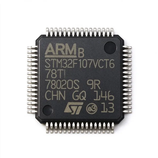
STM32G071RBT6 - 128KB Flash Cortex-M0+ MCU 64MHz | STMicroelectronics
部品番号: STM32G071RBT6 ✓ 生産中| 数量 | 単価 | 小計 |
|---|---|---|
| 1 | $1.6031 | $1.60 |
| 10 | $1.1578 | $11.58 |
| 100 | $1.0242 | $102.42 |
| 500 | $0.9797 | $489.85 |
| 1,000 | $0.9352 | $935.20 |
STM32G071RBT6 概要
A microcontroller (MCU) is a compact integrated circuit that combines a processor core, memory, and programmable peripherals on a single chip to govern a specific operation in an embedded system. The STM32G0 series sits within the broader STM32 family of Arm Cortex-M based MCUs, which in turn belongs to the general taxonomy of 32-bit microcontrollers, embedded processors, and semiconductors. The STM32G0 series targets cost-sensitive and power-efficient mainstream applications while retaining the extensive peripheral ecosystem and development toolchain support of the STM32 platform.
Key features of the STM32G071RBT6 include a 12-bit ADC with hardware oversampling, multiple communication interfaces including I2C, SPI, USART, and LPUART, advanced timers, and an integrated USB 2.0 full-speed device controller. It also integrates a real-time clock (RTC), a CRC calculation unit, a memory protection unit (MPU), and a DMA controller for efficient data transfer, plus a 12-bit DAC for analog signal generation.
Technically, the device is built around a high-performance Arm Cortex-M0+ core featuring a single-cycle multiplier and a nested vectored interrupt controller (NVIC). The 64 MHz core clock, combined with DMA-assisted data movement and hardware oversampling on the ADC, allows the MCU to service demanding sensor, control, and communication workloads while keeping CPU loading and power consumption low. The wide operating temperature range of -40 C to +85 C makes it robust for industrial environments.
Typical applications include industrial control systems, consumer electronics, IoT nodes, smart home automation, battery-powered devices, sensor interfacing, motor control, and USB-connected data logging or firmware update endpoints. The USB device controller enables direct host connectivity, while the analog peripherals support motor current sensing and signal conditioning.
A key design consideration: decouple every VDD pin with 100 nF capacitors placed close to the pins, connect VDDA to a clean analog supply, and configure the BOOT0 pin correctly to select the desired boot mode.
This page synthesizes distributor pricing, drop-in alternatives, and practical design notes not found in the manufacturer datasheet.
ドロップイン代替品: STM32G071RBT6 — 同一パッケージでピン互換。PCBの作り直しが必要な異なるパッケージの部品は除外されています。
このシリーズのバリエーション
同一シリーズでドロップイン互換のモデル: STM32G071RBT6 (同一形状・フットプリント) — 相違点: Package, Timers, Communication Interfaces, Core, ADC.
クイック比較ツール — 並列比較する代替部品を選択:
STM32G081RBT6
✓ 在庫あり
$2.19 / 個
データシートを見る →STM32G071R8T6
📋 参考代替品(カタログ未掲載)
STM32G071CBT6
✓ 在庫あり
価格はお問い合わせください
データシートを見る →STM32G071RBT6 最大定格&電気的特性
| Core | ARM Cortex-M0+ |
| Core Size | 32-bit |
| 最大クロック周波数 | 64 MHz |
| Flash Memory | 128 KB (128K x 8) |
| SRAM | 36 KB |
| Supply Voltage Range | 2.0 V to 3.6 V |
| ADC Resolution | 12-bit |
| DAC Resolution | 12-bit |
| Communication Interfaces | I2C, SPI, USART, LPUART |
| USB Controller | USB 2.0 full-speed device |
| DMA Channels | 5-channel DMA |
| 動作温度 | -40 C to +85 C |
| パッケージ | 64-LQFP (10x10 mm) |
| 実装タイプ | Surface Mount |
| Memory Protection Unit | Yes (MPU) |
| RTC | Yes |
| RoHS ステータス | Compliant |
STM32G071RBT6 64-lqfp (10x10 mm) ピン配置ガイド
STM32G071RBT6 (64-lqfp (10x10 mm) パッケージ) のピン配置。 このデジタルICには、GPIO、通信インターフェース (UART、SPI、I2C)、および電源ピンが含まれています。代替ピン機能と設定オプションについては、メーカーのデータシートを参照してください。組み込みシステム設計とPCBレイアウトに不可欠です。

詳細なピン配置データはありません: STM32G071RBT6.
詳細は データシート をご参照ください。
主な用途
STM32G071RBT6 の用途: 6 件s: Industrial Control Systems, IoT and Smart Home Devices, USB-Connected Data Logging, Motor Control, Consumer Electronics, Sensor Interfacing and Instrumentation.
Industrial Control Systems
The STM32G071RBT6 fits industrial control nodes because its 64 MHz Cortex-M0+ core, 128 KB Flash, and advanced timers can handle deterministic control loops and communication simultaneously. The 12-bit ADC with hardware oversampling provides high-resolution current and voltage feedback for closed-loop control, while the -40 C to +85 C operating range and wide 2.0 V to 3.6 V supply tolerance survive industrial electrical environments. In typical circuits the MCU runs the control loop with timer-generated PWM outputs and DMA-assisted ADC sampling, keeping CPU loading low; the 5-channel DMA moves sensor data without core intervention, delivering quantifiable real-time margin for fieldbus handling.
おすすめ
IoT and Smart Home Devices
For IoT nodes and smart home products, the STM32G071RBT6 aligns well: its 2.0 V to 3.6 V supply range suits battery and USB-powered designs, and the 64 MHz Cortex-M0+ core with 128 KB Flash and 36 KB RAM provides headroom for connectivity stacks and OTA firmware staging. The LPUART allows low-power communication with wireless modules while the core sleeps, and the RTC keeps time-of-day scheduling alive in low-power modes. The integrated USB 2.0 full-speed device controller enables direct configuration and data logging to hosts without an external bridge IC, reducing BOM cost; the MPU and CRC unit add data-integrity support for firmware update paths.
おすすめ
USB-Connected Data Logging
The STM32G071RBT6's integrated USB 2.0 full-speed device controller makes it a natural single-chip solution for USB data loggers and firmware-update endpoints. Sensor data captured through the 12-bit ADC or USART/SPI peripherals is buffered in the 36 KB SRAM and streamed over USB, with the 5-channel DMA offloading transfers so the 64 MHz core can format packets and manage the protocol stack. Because the USB controller is on-chip, no external USB bridge is required, cutting BOM cost and board area; the 128 KB Flash accommodates USB class stacks alongside application code, and the CRC unit supports in-application firmware integrity checking before bootloader handoff.
おすすめ
Motor Control
In small motor control applications such as fans, pumps, and consumer appliance drives, the STM32G071RBT6 offers advanced timers for complementary PWM generation, a 12-bit ADC for phase-current sampling synchronized to PWM events, and a 12-bit DAC for reference or setpoint generation. The 64 MHz Cortex-M0+ core executes field-oriented or trapezoidal control loops with low-level interrupt latency managed by the NVIC, while DMA handles ADC result retrieval without CPU intervention. The -40 C to +85 C temperature range covers appliance and industrial drive environments; designers should budget ADC input filtering and shunt sizing to exploit the hardware oversampling feature for noise reduction.
おすすめ
Consumer Electronics
Cost-sensitive consumer products such as small appliances, chargers, toys, and accessories benefit from the STM32G071RBT6's mainstream positioning: 64 MHz Cortex-M0+ performance, 128 KB Flash, and a rich peripheral set at a commodity price point (from about $1.28 at volume as of 2026-09-06). The I2C and SPI interfaces connect touch controllers, displays, and sensors, while timers drive LEDs, buzzers, and simple actuation. Its 2.0 V to 3.6 V operation supports both USB-powered and battery-powered consumer form factors. Compared with 8-bit MCUs, the 32-bit core with DMA and hardware oversampling ADC enables features such as capacitive touch sensing and precise battery monitoring at similar BOM cost.
おすすめ
Sensor Interfacing and Instrumentation
The STM32G071RBT6 serves as a sensor-hub and measurement frontend because its 12-bit ADC with hardware oversampling achieves higher effective resolution without CPU cost, and its 12-bit DAC plus comparators support closed-loop analog conditioning. Multiple USARTs, LPUART, I2C, and SPI ports allow simultaneous interfacing with digital sensors and radios, while the 5-channel DMA streams conversion results into the 36 KB SRAM. The VDDA pin requires a clean analog supply decoupled per datasheet guidance (100 nF on each VDD, 1 uF on VREF+) to realize the ADC's accuracy; with this layout discipline the device provides stable, low-drift measurements for environmental and industrial sensors.
おすすめ
おすすめ製品の概要
エンジニアリング参考データ: STM32G071RBT6 — 比較、設計ガイダンス、コンプライアンス情報。
選定ガイド
代替品との比較
| パラメータ | この製品 | STM32G071R8T6 | STM32G081RBT6 | STM32G071CBT6 |
|---|---|---|---|---|
| Package | 64-LQFP (10x10 mm) | 64-LQFP (10x10 mm) - same | 64-LQFP (10x10 mm) - same | 48-LQFP (7x7 mm) - smaller footprint |
| Brand | STMicroelectronics | STMicroelectronics | STMicroelectronics | STMicroelectronics |
| Core / Frequency | Arm Cortex-M0+ @ 64 MHz | Arm Cortex-M0+ @ 64 MHz | Arm Cortex-M0+ @ 64 MHz | Arm Cortex-M0+ @ 64 MHz |
| Flash Memory | 128 KB | 64 KB | 128 KB | 128 KB |
| SRAM | 36 KB | 36 KB | 36 KB | 36 KB |
| USB Device Controller | USB 2.0 full-speed device | USB 2.0 full-speed device | USB 2.0 full-speed device | USB 2.0 full-speed device |
| Hardware Security (AES) | No | No | Yes (AES accelerator) | No |
| Operating Temperature | -40 C to +85 C | -40 C to +85 C | -40 C to +85 C | -40 C to +85 C |
主な差別化要因
- On-chip USB 2.0 full-speed device at mainstream price (vs STM32G071R8T6)
- Larger 128 KB Flash with same footprint as the G081 (vs STM32G081RBT6)
- General-purpose mainstream SKU (vs STM32G071CBT6)
設計ノート
Decouple every VDD pin with 100 nF ceramic capacitors placed as close as possible to the pin, each with a low-impedance path to the VSS plane. Connect VDDA to a clean, filtered analog supply and decouple the VREF+ pin with a 1 uF capacitor to preserve 12-bit ADC accuracy. The supply range is 2.0 V to 3.6 V; avoid exceeding 3.6 V absolute maximum. Estimated: at 64 MHz with typical peripheral loading, core current is in the low tens of mA, so a linear regulator from 5 V is acceptable for USB-powered designs.
Configure the BOOT0 pin correctly to select the boot mode: tied low for execution from main Flash, pulled high (with nBOOT option bits considered) for the system bootloader used in production programming via USART or USB. Misconfigured BOOT0 is one of the most common bring-up failures on STM32G0 boards. Also verify the NRST pin (shared with PG10) pull-up configuration, and do not float unused PA13/PA14 SWD pins if debugger access must be retained after production.
For the 64-LQFP (10x10 mm) footprint, place the 100 nF decoupling capacitors on the opposite side of the board directly beneath each VDD pin or on the same side within 2 mm, and use a solid ground plane. Keep the VDDA/VREF+ analog supply routing away from USB D+/D- and PWM switching nets to protect ADC accuracy. Route USB D+/D- as a 90-ohm differential pair with matched lengths when the USB full-speed device port is used.
コンプライアンス情報
RoHS compliant per distributor listings (DigiKey, LCSC). REACH, halogen-free, and conflict minerals status should be confirmed on the ST compliance portal.


