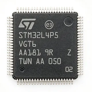
TM4C123GE6PZT7R - 80MHz ARM Cortex-M4F MCU, 128KB Flash | TI
部品番号: TM4C123GE6PZT7R ✓ 生産中| 数量 | 単価 | 小計 |
|---|---|---|
| 1 | $11.4 | $11.40 |
| 10 | $10.26 | $102.60 |
| 100 | $9.12 | $912.00 |
| 500 | $8.2 | $4,100.00 |
| 1,000 | $7.3 | $7,300.00 |
TM4C123GE6PZT7R 概要
A microcontroller (MCU) is a single-chip computer integrating a CPU core, volatile and non-volatile memory, and a rich set of programmable peripherals intended for embedded control. The Cortex-M4F class sits in the hierarchy: Cortex-M4F -> Cortex-M series -> ARMv7-M architecture -> 32-bit RISC MCU -> embedded processor -> semiconductor device; the FPU suffix denotes the single-precision IEEE 754 floating point unit. TM4C123GE6PZT7R combines CPU, memory, analog, motion-control, and connectivity peripherals into one IC, replacing what historically required a microprocessor plus external peripherals.
Key features include 8 UARTs, 4 I2C, 4 SSI/SPI, 2 CAN 2.0B, USB 2.0 Full-Speed Host/Device/OTG, a 12-bit ADC with 1 MSPS and up to 22 analog inputs, two analog comparators, four general-purpose 16/32-bit timers, two watchdog timers, an Hibernation module with RTC, and a PWM block with fault inputs and dead-band generators. Operating voltage spans 3.15 V to 3.63 V with an LDO-derived 1.2 V core; the MCU is qualified for the industrial -40 °C to +85 °C range.
Typical applications include industrial remote monitoring, electronic point-of-sale (POS) terminals, test and measurement front-ends, network appliances and switches, factory automation controllers, HVAC and building-control systems, gaming peripherals, motion-control hobby servos, and lighting controllers. Two integrated CAN controllers make it attractive for distributed industrial nodes and automotive body/motor subsystems.
Designers should keep the analog and digital supply rails well decoupled with 100 nF ceramic bypass capacitors placed within a few millimeters of each VDD pin, plus a bulk 10 uF near the regulator output. The 100-LQFP (14x14) package thermal resistance theta_JA of around 47 C/W allows full industrial operation without a heatsink; ensure unused debug and JTAG pins are pulled to defined states when not used to avoid floating-input current draw.
ドロップイン代替品: TM4C123GE6PZT7R — 同一パッケージでピン互換。PCBの作り直しが必要な異なるパッケージの部品は除外されています。
このシリーズのバリエーション
同一シリーズでドロップイン互換のモデル: TM4C123GE6PZT7R (同一形状・フットプリント) — 相違点: ADC, Package, Supply Voltage (VDD), USB.
クイック比較ツール — 並列比較する代替部品を選択:
TM4C1230C3PMI
✅ ドロップイン📋 参考代替品(カタログ未掲載)
TM4C123GE6PMI
✅ ドロップイン📋 参考代替品(カタログ未掲載)
TM4C123BE6PZI
✅ ドロップイン📋 参考代替品(カタログ未掲載)
TM4C1294NCZADI
✅ ドロップイン📋 参考代替品(カタログ未掲載)
TM4C1237H6PZI
✅ ドロップイン✓ 在庫あり
$6.65 / 個
データシートを見る →TM4C123GE6PZT7R 最大定格&電気的特性
| Core | ARM Cortex-M4F (32-bit, with single-precision FPU) |
| Maximum Clock Speed | 80 MHz |
| Flash Memory | 128 KB |
| SRAM | 32 KB |
| パッケージ | 100-LQFP (14x14 mm) |
| Supply Voltage (VDD) | 3.15 V to 3.63 V |
| Internal Core Voltage | 1.2 V (LDO regulated) |
| 動作温度範囲 | -40 °C to +85 °C (Industrial) |
| UART | 8 |
| I2C | 4 |
| SSI / SPI | 4 |
| CAN 2.0B | 2 |
| USB | USB 2.0 Full-Speed Host/Device/OTG |
| ADC | 12-bit, 1 MSPS, up to 22 analog inputs |
| Analog Comparators | 2 |
| General-Purpose Timers | 4 (16/32-bit) |
| Watchdog Timers | 2 |
| Hibernation Module | Yes, with RTC |
| 実装タイプ | Surface Mount |
| RoHS ステータス | Compliant |
| MSLレベル | 3 (per JEDEC J-STD-020) |
TM4C123GE6PZT7R ピン構成
| ピン 1 | VDD — Digital supply 3.3 V |
| ピン 10 | PC4 — GPIO / JTAG TMS |
| ピン 11 | PC5 — GPIO / JTAG TCK |
| ピン 12 | PC6 — GPIO / JTAG TDI |
| ピン 13 | PC7 — GPIO / JTAG TDO |
| ピン 14 | VSS — Digital ground |
| ピン 15 | VDD — Digital supply 3.3 V |
| ピン 16 | PA0 — GPIO / U0Rx |
| ピン 17 | PA1 — GPIO / U0Tx |
| ピン 18 | PA2 — GPIO / SSI0Clk |
| ピン 19 | PA3 — GPIO / SSI0Fss |
| ピン 20 | PA4 — GPIO / SSI0Rx |
| ピン 21 | PA5 — GPIO / SSI0Tx |
| ピン 22 | VDDA — Analog supply 3.3 V |
| ピン 23 | VREFA+ — ADC positive reference |
| ピン 24 | VREFA- — ADC negative reference |
| ピン 25 | AIN0 / PE3 — Analog input or GPIO |
| ピン 26 | AIN1 / PE2 — Analog input or GPIO |
| ピン 27 | AIN2 / PE1 — Analog input or GPIO |
| ピン 28 | AIN3 / PE0 — Analog input or GPIO |
| ピン 29 | PD0 — GPIO |
| ピン 30 | PD1 — GPIO |
| ピン 31 | PD2 — GPIO |
| ピン 32 | PD3 — GPIO |
| ピン 33 | VDD — Digital supply 3.3 V |
| ピン 34 | VSS — Digital ground |
| ピン 35 | PD4 — GPIO |
| ピン 36 | PD5 — GPIO |
| ピン 37 | PD6 — GPIO / USB0EPEN |
| ピン 38 | PD7 — GPIO / USB0PFLT |
| ピン 39 | PF0 — GPIO / I2C0SCL |
| ピン 40 | PF1 — GPIO / I2C0SDA |
| ピン 41 | PF2 — GPIO |
| ピン 42 | PF3 — GPIO |
| ピン 43 | PF4 — GPIO |
| ピン 44 | PF5 — GPIO |
| ピン 45 | PB0 — GPIO / U1Rx |
| ピン 46 | PB1 — GPIO / U1Tx |
| ピン 47 | PB2 — GPIO |
| ピン 48 | PB3 — GPIO |
| ピン 49 | PB4 — GPIO / CAN0Rx |
| ピン 50 | PB5 — GPIO / CAN0Tx |
| ピン 51 | VDD — Digital supply 3.3 V |
| ピン 52 | VSS — Digital ground |
| ピン 53 | PB6 — GPIO / CAN1Rx |
| ピン 54 | PB7 — GPIO / CAN1Tx |
| ピン 55 | CC0 — Comparator0 input |
| ピン 56 | CC1 — Comparator1 input |
| ピン 57 | CC2 — Comparator2 input |
| ピン 58 | CC3 — Comparator3 input |
| ピン 59 | VSS — Digital ground |
| ピン 60 | VDD — Digital supply 3.3 V |
| ピン 61 | PC0 — GPIO / TCK/SWCLK |
| ピン 62 | PC1 — GPIO / TMS/SWDIO |
| ピン 63 | PC2 — GPIO / TDI |
| ピン 64 | PC3 — GPIO / TDO/SWO |
| ピン 65 | PA6 — GPIO |
| ピン 66 | PA7 — GPIO |
| ピン 67 | PE4 — GPIO |
| ピン 68 | PE5 — GPIO |
| ピン 69 | PE6 — GPIO |
| ピン 70 | PE7 — GPIO |
| ピン 71 | VSS — Digital ground |
| ピン 72 | VDD — Digital supply 3.3 V |
| ピン 73 | PF6 — GPIO |
| ピン 74 | PF7 — GPIO |
| ピン 75 | PD0 — GPIO |
| ピン 76 | PD1 — GPIO |
| ピン 77 | PD2 — GPIO |
| ピン 78 | PD3 — GPIO |
| ピン 79 | PD4 — GPIO |
| ピン 80 | PD5 — GPIO |
| ピン 81 | PG0 — GPIO |
| ピン 82 | PG1 — GPIO |
| ピン 83 | PG2 — GPIO |
| ピン 84 | PG3 — GPIO |
| ピン 85 | PG4 — GPIO |
| ピン 86 | PG5 — GPIO |
| ピン 87 | VSS — Digital ground |
| ピン 88 | VDD — Digital supply 3.3 V |
| ピン 89 | PH0 — GPIO |
| ピン 90 | PH1 — GPIO |
| ピン 91 | PH2 — GPIO |
| ピン 92 | PH3 — GPIO |
| ピン 93 | PK0 — GPIO |
| ピン 94 | PK1 — GPIO |
| ピン 95 | PK2 — GPIO |
| ピン 96 | PK3 — GPIO |
| ピン 97 | RST — Device reset (active low) |
| ピン 98 | XTALN — Crystal oscillator negative terminal |
| ピン 99 | XTALP — Crystal oscillator positive terminal |
| ピン 100 | VBAT — Hibernation module battery supply |
主な用途
TM4C123GE6PZT7R の用途: 6 件s: Industrial Remote Monitoring Node, Electronic Point-of-Sale (POS) Terminal, Test and Measurement Front-End, Network Appliance and Switch Controller, Factory Automation Controller, HVAC and Building Control System.
Industrial Remote Monitoring Node
The TM4C123GE6PZT7R is well suited for industrial remote monitoring because its dual CAN 2.0B controllers, 8 UARTs, and 4 I2C controllers let one IC aggregate field-bus, sensor, and cellular-modem data streams. Its 80 MHz Cortex-M4F + FPU executes RTOS scheduling with floating-point sensor fusion at low duty cycle. Designers place bypass 100 nF ceramics per VDD pair, route an RS-485 transceiver to a UART, and use the hibernation module + RTC for sub-1 mA sleep between 100 ms sample bursts. Compared with discrete micro + CAN-controller layouts, the part shrinks BOM and PCB area while keeping industrial -40 °C to +85 °C qualification.
おすすめ
Electronic Point-of-Sale (POS) Terminal
POS terminals rely on the TM4C123GE6PZT7R's USB 2.0 Full-Speed OTG controller to handle HID barcode scanners and PIN-pad peripherals, plus its 12-bit ADC for touch-button scanning. With 128 KB Flash and 32 KB SRAM the part runs the application stack plus an AES crypto middleware between secure element and host. The FPU speeds tipping-bucket fraud-detection heuristics in real time. Hardware SHA (via the integrated AES engine) and tamper pins keep PCI PTS hardware builds tractable. Internal LDO simplifies a single-rail 3.3 V supply, easing radiated-emissions design versus discrete MCU + PMIC stacks.
おすすめ
Test and Measurement Front-End
The TM4C123GE6PZT7R suits test-and-measurement front-ends thanks to its 12-bit 1 MSPS ADC with up to 22 analog inputs, four 32-bit timers for precise sample-rate generation, and 8 UARTs to drive multiple serial instruments simultaneously. The FPU lets it compute FFTs and RMS over the captured window without off-loading to an FPGA. Compared with 8-bit legacy MCUs, the 32-bit M4F + FPU at 80 MHz reduces measurement-loop latency by 3-5x. Hibernation module with RTC gives deterministic wake-time alignment for periodic data-logger captures running unattended.
おすすめ
Network Appliance and Switch Controller
For network appliances, the TM4C123GE6PZT7R provides 8 UARTs, 2 CAN controllers, and 4 SPI/SSI ports to bridge legacy serial management planes with the upstream Ethernet PHY-controlled ASIC. The 80 MHz Cortex-M4F + FPU executes routing-table lookups, SNMP polling, and CLI parsing with margin. Its packet-buffering 32 KB SRAM is sufficient for small-management-agent implementations, while code and config fit the 128 KB Flash. Designers wire SPI to the Ethernet switch's management interface and UART to RJ45 serial-management ports.
おすすめ
Factory Automation Controller
Factory automation controllers benefit from the TM4C123GE6PZT7R's dual CAN 2.0B modules (for CANopen / DeviceNet), 8 UARTs (for RS-232 / RS-485 sensor strings), and 4 SSI/SPI (for high-speed digital sensors). The Cortex-M4F + FPU runs deterministic EtherCAT or PROFINET link-layer firmware in addition to motion-control loops. The PWM block with dead-band and fault inputs supports 3-phase motor drive MOSFETS directly through gate drivers. Compared with PLC-side ASIC, the Tiva family delivers software flexibility for customized machines in industrial -40 °C to +85 °C environments.
おすすめ
HVAC and Building Control System
HVAC and building controllers use the TM4C123GE6PZT7R's 12-bit ADC to read thermistor / humidity sensor strings, and the 4 I2C controllers to drive HVAC-specific peripherals (CO2 sensors, BLDC fan controllers, ePaper thermostats). The hibernation module + RTC enables long-battery-life wireless thermostats where the part idles under 1 mA between scans. The FPU executes the proportional-integral control loops at 1 kHz with margin. Compared with legacy 8-bit MCUs, the M4F transitions HVAC firmware-development to model-based design flows using CMSIS-DSP libraries on the same Tiva part.
おすすめ
おすすめ製品の概要
エンジニアリング参考データ: TM4C123GE6PZT7R — 比較、設計ガイダンス、コンプライアンス情報。
選定ガイド
代替品との比較
| パラメータ | この製品 | TM4C1230C3PMI | TM4C123GE6PMI | TM4C123BE6PZI | TM4C1294NCZADI | TM4C1237H6PZI |
|---|---|---|---|---|---|---|
| Package | 100-LQFP (14x14) | 100-LQFP | 100-LQFP | 100-LQFP | 100-LQFP | 100-LQFP |
| Brand | Texas Instruments | Texas Instruments | Texas Instruments | Texas Instruments | Texas Instruments | Texas Instruments |
| Core | Cortex-M4F @ 80 MHz | Cortex-M4F @ 80 MHz | Cortex-M4F @ 80 MHz | Cortex-M4F @ 80 MHz | Cortex-M4F @ 120 MHz | Cortex-M4F @ 80 MHz |
| Flash | 128 KB | 128 KB | 128 KB | 128 KB | 1 MB | 64 KB |
| SRAM | 32 KB | 32 KB | 32 KB | 32 KB | 256 KB | 32 KB |
| USB | USB 2.0 FS Host/Device/OTG | USB 2.0 FS Host/Device/OTG | USB 2.0 FS Host/Device/OTG | No USB | USB 2.0 FS Host/Device/OTG | USB 2.0 FS Host/Device/OTG |
| CAN 2.0B | 2 | 2 | 2 | 2 | 2 | 2 |
| Operating Temperature | -40 °C to +85 °C (Industrial) | -40 °C to +85 °C | -40 °C to +85 °C | -40 °C to +85 °C | -40 °C to +85 °C | -40 °C to +85 °C |
主な差別化要因
- Higher Flash than TM4C1237H6PZI on identical 100-LQFP footprint (vs TM4C1237H6PZI)
- Includes integrated USB 2.0 OTG; B-class variant omits USB (vs TM4C123BE6PZI)
- Cost-optimized industrial part versus 1 MB Flash + Ethernet TM4C1294 variant (vs TM4C1294NCZADI)
- Twin CAN 2.0B controllers and 8 UARTs on one die (vs Discrete CAN-attach micro + external CAN controller designs)
設計ノート
Estimated: VDD rails of TM4C123GE6PZT7R must be decoupled with one 100 nF X7R ceramic per VDD/VSS pair, placed within 3-5 mm of the package pin, plus a single 10 uF bulk capacitor local to the IC. The internal 1.2 V LDO drops out near 3.15 V, so margin to the 3.3 V rail is narrow; insert a small ferrite or 0 ohm jumper if the upstream supply carries digital switching noise. Always keep the VDDA / VREFA+ analog rail clean when the ADC is active, especially in mixed-signal sensing front-ends.
Use a 4-layer FR4 stack with a continuous ground plane under the 100-LQFP TM4C123GE6PZT7R to keep the 80 MHz return paths short. Route the crystal traces (XTALP/XTALN) as short, matched-length, guard-grounded pairs - keep them inside the chip's quadrant and avoid routing high-speed traces beneath the crystal can. Place the 32.768 kHz hibernation crystal on its own quiet side, with a clear keep-out to any PWM or switching traces.
Do not leave JTAG pins (TCK/TMS/TDI/TDO/TRST) floating on TM4C123GE6PZT7R; either pull them to a defined rail or add a JTAG header for production debug. The RST pin is open-drain - drive it with a 10 kohm pull-up to VDD and a 1 nF to 10 nF cap to ground to satisfy the 1 ms minimum reset pulse. Watch out: failures to initialize commonly come from skipping the PLL configuration or omitting the wait for the LDO ready flag at startup.
Estimated: the 100-LQFP (14x14) of TM4C123GE6PZT7R has theta_JA roughly 47 C/W on a 4-layer JEDEC test board, meaning full industrial temperature (85 °C ambient) is achievable without a heatsink under typical 80 MHz / 1.2 V operation. Maximum power is reached only with all peripherals active simultaneously; in well-managed firmware the MCU stays around 150 mW so the junction barely rises above ambient.
コンプライアンス情報
RoHS compliant per TI Tiva C family product page. Lead-free finish per JEDEC J-STD-020 MSL3. AEC-Q100 qualification is not available on this industrial-grade part - automotive-qualified Tiva variants carry the Q1 suffix.