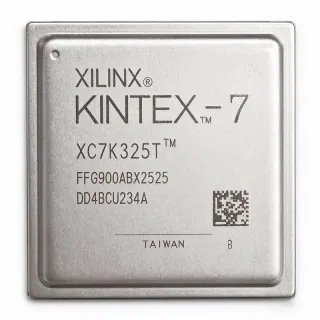
XCKU13P-3FFVE900E - Kintex UltraScale+ FPGA 900-BBGA | AMD
部品番号: XCKU13P-3FFVE900E ✓ 生産中XCKU13P-3FFVE900E 概要
An FPGA is a programmable semiconductor whose internal digital logic, interconnect, memory resources, and peripheral blocks are configured after manufacture. The Kintex UltraScale+ family belongs to the broader field-programmable gate array category, then to programmable-logic devices and semiconductor ICs. This hierarchy places the XCKU13P-3FFVE900E in applications where hardware parallelism, reconfigurable architecture, and deterministic digital signal processing are more valuable than the simplicity of a fixed-function controller.
The XCKU13P-3FFVE900E is distinguished by its -3 speed designation, the XCKU13P family designation, and its 900-BBGA FCBGA construction. Distributor catalog data identifies it as the Kintex UltraScale+ series and confirms a 900-terminal ball package with a square package shape. The exact programmable logic elements, transceivers, I/O standards, memory resources, power characteristics, and temperature limits are not stated in the available catalog records and must be taken from the manufacturer datasheet before design release.
Because the device uses a large ball-grid array, PCB construction demands careful escape-routing planning. Every signal reaching the FPGA must be routed through the ball matrix, including power, ground, configuration pins, clock inputs, and high-speed I/O. Layer-count selection, via-in-pad construction, solder-mask design, and component placement should therefore be evaluated together rather than as independent fabrication choices.
Typical FPGA implementation categories include parallel signal processing, network and communications equipment, industrial control, test and measurement, high-speed data acquisition, and accelerator logic. These uses fit the programmable architecture of the Kintex UltraScale+ family, although project-specific timing closure depends on the complete clocking, pin, and power configuration.
The -3 grade is appropriate when the design requires a higher performance grade within the same package and device family, but grade substitution must be validated against the target operating conditions, timing margins, power budget, and system qualification plan. Use the AMD package pinout files and the manufacturer datasheet to confirm every ball assignment before layout.
This page combines manufacturer-family positioning, verified package information, commercial availability data, drop-in same-package alternatives, comparison parameters, and PCB-design guidance. It also distinguishes catalog-confirmed facts from parameters that require direct confirmation in the official device documentation, helping engineers move from part selection to a controlled hardware design.
ドロップイン代替品: XCKU13P-3FFVE900E — 同一パッケージでピン互換。PCBの作り直しが必要な異なるパッケージの部品は除外されています。
このシリーズのバリエーション
同一シリーズでドロップイン互換のモデル: XCKU13P-3FFVE900E (同一形状・フットプリント) — 相違点: Package Type, Product Type, Speed Grade.
XCKU13P-3FFVE900I
✅ ドロップイン📋 参考代替品(カタログ未掲載)
XCKU13P-2FFVE900I
✅ ドロップイン価格はお問い合わせください
データシートを見る →XCKU13P-1FFVE900E
✅ ドロップイン価格はお問い合わせください
データシートを見る →XCKU13P-2FFVE900I
✅ ドロップイン価格はお問い合わせください
データシートを見る →XCKU13P-FFVE900
✅ ドロップイン📋 参考代替品(カタログ未掲載)
XCKU13P-3FFVE900E 最大定格&電気的特性
| Manufacturer | AMD / Xilinx |
| Product Type | Field Programmable Gate Array (FPGA) |
| Device Family | Kintex UltraScale+ |
| Series | XCKU13P |
| Speed Grade | -3 |
| Package Code | BGA |
| Package Type | 900-BBGA, FCBGA |
| Number of Terminals | 900 |
| Terminal Form | Ball |
| Package Shape | Square |
| 実装タイプ | Surface Mount |
| Programmable Logic Type | FPGA |
| RoHS ステータス | ROHS |
XCKU13P-3FFVE900E square ピン配置ガイド
XCKU13P-3FFVE900E (square パッケージ) のピン配置。 このデジタルICには、GPIO、通信インターフェース (UART、SPI、I2C)、および電源ピンが含まれています。代替ピン機能と設定オプションについては、メーカーのデータシートを参照してください。組み込みシステム設計とPCBレイアウトに不可欠です。

詳細なピン配置データはありません: XCKU13P-3FFVE900E.
詳細は データシート をご参照ください。
主な用途
XCKU13P-3FFVE900E の用途: 6 件s: High-Speed Data Acquisition, Network Packet Processing, Industrial Control Systems, Test and Measurement Equipment, Communications Infrastructure, Aerospace and Defense Prototyping.
High-Speed Data Acquisition
The XCKU13P-3FFVE900E is appropriate for parallel data-acquisition systems that combine wide input channels with real-time digital processing. Its programmable Kintex UltraScale+ architecture allows acquisition, filtering, thresholding, and data reduction to be consolidated in one device instead of split across multiple fixed-function blocks. The 900-BBGA FCBGA package also offers dense access to the device's ball matrix, although usable I/O count and supported interface standards must be confirmed in the manufacturer documentation. Design the PCB with short, matched escape routes and verify timing closure with the intended clocking architecture before release.
おすすめ
Network Packet Processing
The XCKU13P-3FFVE900E can support programmable packet-processing, protocol-conversion, and traffic-management functions where parallel logic and flexible interfaces are valuable. Engineers can implement framing, classification, filtering, and buffering logic in the Kintex UltraScale+ fabric while retaining the option to revise the design through device reconfiguration. Exact line rates and transceiver availability depend on the device resource configuration, so the AMD datasheet and Vivado implementation results must confirm the target interface. High-speed board design also requires controlled impedance, continuous reference planes, and careful power-delivery planning.
おすすめ
Industrial Control Systems
The XCKU13P-3FFVE900E suits industrial controllers that require deterministic parallel logic, multiple I/O functions, or hardware-level timing behavior. A programmable FPGA can implement motion sequencing, sensor fusion, safety interlocks, and communication adaptation within a compact system, while the -3 designation provides a defined higher performance tier for timing-critical paths. The designer must still verify I/O standards, operating-temperature requirements, and the final ordering suffix against the AMD documentation. The 900-ball package requires an assembly process qualified for its thermal and solder-joint requirements.
おすすめ
Test and Measurement Equipment
The XCKU13P-3FFVE900E can be used in test and measurement instruments that combine trigger logic, pattern generation, digital signal conditioning, and real-time analysis. Parallel programmable resources allow multiple measurement channels to share one processing fabric, reducing dependence on fixed-function converters and controllers. Achieving the intended result requires verified clock specifications, I/O rates, supported voltage standards, and deterministic timing from the manufacturer documentation. PCB implementation should account for the FCBGA thermal pad, decoupling distribution, and the large escape-routing area needed by the 900-ball footprint.
おすすめ
Communications Infrastructure
The XCKU13P-3FFVE900E is suitable for communications infrastructure that uses programmable logic for aggregation, channelization, protocol adaptation, or low-latency forwarding. Its Kintex UltraScale+ position and 900-BBGA construction provide a platform for designs that benefit from parallel processing and extensive package connectivity. Interface speed, transceiver use, clocking topology, and power limits must be confirmed in the AMD datasheet before schematic capture. A production layout should also include complete ball-assignment review, reference-plane continuity, and power-plane segmentation around high-speed and high-current regions.
おすすめ
Aerospace and Defense Prototyping
The XCKU13P-3FFVE900E can be evaluated for aerospace, defense, and rugged embedded prototypes that benefit from programmable parallel logic and deterministic processing. The device family offers flexible implementation resources, but a laboratory-grade part is not automatically qualified for a flight program. Qualification status, temperature range, screening level, reliability documentation, and ordering-code meaning must be reviewed with the manufacturer. Engineering development should preserve footprint flexibility, define a controlled configuration process, and plan for long-term supply and traceability requirements.
おすすめ
おすすめ製品の概要
エンジニアリング参考データ: XCKU13P-3FFVE900E — 比較、設計ガイダンス、コンプライアンス情報。
選定ガイド
代替品との比較
| パラメータ | この製品 | XCKU13P-3FFVE900I | XCKU13P-2FFVE900I | XCKU13P-1FFVE900E | XCKU13P-2FFVE900I | XCKU13P-FFVE900 |
|---|---|---|---|---|---|---|
| Brand | AMD | AMD | AMD | AMD | AMD | AMD |
| Package | 900-BBGA, FCBGA | 900-BBGA, FCBGA - same | 900-BBGA, FCBGA - same | 900-BBGA, FCBGA - same | 900-BBGA, FCBGA - same | 900-BBGA, FCBGA - same |
| Device Family | XCKU13P Kintex UltraScale+ | XCKU13P Kintex UltraScale+ | XCKU13P Kintex UltraScale+ | XCKU13P Kintex UltraScale+ | XCKU13P Kintex UltraScale+ | XCKU13P Kintex UltraScale+ |
| Number of Terminals | 900 | 900 | 900 | 900 | 900 | 900 |
| Programmable Logic Type | Field Programmable Gate Array | Field Programmable Gate Array | Field Programmable Gate Array | Field Programmable Gate Array | Field Programmable Gate Array | Field Programmable Gate Array |
| Ordering Suffix | E | I | I | E | I | No E or I suffix shown |
主な差別化要因
- Highest listed speed grade within the compared XCKU13P package options (vs XCKU13P-1FFVE900E)
- Same 900-BBGA footprint as the lower-speed family alternatives (vs XCKU13P-2FFVE900I)
- Catalog-confirmed 900-terminal surface-mount construction (vs XCKU13P-FFVE900)
設計ノート
Plan the 900-BBGA escape routing before schematic-to-layout handoff. Import the official AMD package-pinout file into the PCB library and verify every ball number against the selected device ordering code. The package is large and dense, so component placement, layer transitions, reference-plane continuity, and thermal-via placement should be optimized together. Avoid hand-transcribed ball maps, which create a substantial risk of silent connectivity errors.
Build the power tree around the voltage rails and current limits stated in the AMD device documentation. Place bulk energy-storage components near the device's power-entry structure and distribute high-frequency decoupling across the power and ground ball fields. Validate return-current paths under simultaneous switching activity rather than only under a static operating condition. Confirm the selected -3 speed grade against the final power budget because performance and thermal requirements are design-specific.
The 900-ball FCBGA depends on a controlled thermal path through its package substrate and PCB copper. Model the board, thermal-via array, heat spreader, and enclosure as one system, then select the assembly method from the manufacturer package information. Validate junction-temperature targets with the actual operating profile. Keep the thermal design separate from electrical simulation, but tie them together through component placement and the location of power-delivery structures.
Do not treat speed-grade or ordering-suffix changes as automatic substitutions. A lower -1 or -2 grade can alter timing margins, power consumption, and qualification conditions, while the final E or I character can carry ordering distinctions. Before substitution, compare the complete AMD ordering table, rerun implementation timing, verify temperature and qualification requirements, and confirm that the package pinout remains identical.
コンプライアンス情報
The LCSC catalog record marks the XCKU13P-3FFVE900E as ROHS. No verified information was provided for REACH, AEC-Q100, halogen-free status, or conflict-minerals compliance.