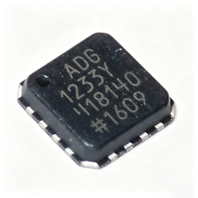
ADF4113BRU
ADF4113BRU - 4 GHz Integer-N RF PLL | Analog Devices
The Analog Devices ADF4113BRU is a single integer-N RF frequency synthesizer with a 4.0 GHz maximum operating frequency, programmable prescaler and charge pump, and a 16-pin TSSOP package. The device combines a low-noise digital phase-frequency detector, precision charge pump, programmable reference divider, programmable A and B counters, and a dual-modulus prescaler for local-oscillator generation in wireless receivers and transmitters. Its programmable architecture lets designers divide down a stable reference source and synthesize the required carrier frequency while controlling channel spacing through the reference divider, counters, and prescaler settings.
An integer-N PLL is a frequency-synthesizer category in which the feedback prescaler and integer counters establish the output frequency while the phase-frequency detector and charge-pump network close the loop around a voltage-controlled oscillator. The ADF4110 family therefore belongs to the broader hierarchy of clock and timing ICs, frequency synthesizers, phase-locked loops, RF signal-chain ICs, and semiconductors. Integer-N operation simplifies control compared with fractional-N architectures, while the maximum RF input rate enables high-frequency local-oscillator designs when the VCO and loop bandwidth are suitable.
The ADF4113BRU supports RF synthesis up to 4.0 GHz and includes programmable dual-modulus prescaling, programmable charge-pump currents, a separate charge-pump supply, and a programmable reference divider. The family documentation also identifies 3 V system operation. Separate charge-pump supply capability allows extended tuning-voltage headroom, which is useful when the external VCO requires a tuning range beyond the main supply rail. The programmable charge-pump current provides another control point for loop dynamics and reference-spur trade-offs.
The internal signal path uses a low-noise digital phase-frequency detector, precision charge pump, programmable reference divider, A and B counters, and P/P+1 dual-modulus prescaler. This arrangement is intended for integer-N local oscillators in RF upconversion and downconversion paths. The 16-TSSOP body is 4.40 mm wide and corresponds to the 0.173-inch package description listed by DigiKey. Package, lead finish, and orderable suffix must be checked against the Analog Devices ordering guide before substituting an alternative.
Typical uses include GSM and other wireless receiver or transmitter local oscillators, RF upconversion and downconversion blocks, communications test equipment, and frequency-generation subsystems. In such systems, the reference divider can reduce a high-frequency reference before comparison with the divided VCO output. The A counter, B counter, and dual-modulus prescaler determine the integer multiplication relationship, while the charge pump and external loop filter translate phase error into VCO tuning voltage.
The principal design constraint is loop stability. Component values for the charge-pump, loop filter, and VCO must be derived for the actual reference frequency, target output frequency, prescaler, phase margin, and tuning range. RF routing also requires short, controlled-impedance paths, solid return planes, and careful separation between sensitive synthesizer inputs and high-energy clock or switching nodes. The ADF4113 datasheet family should be consulted for the complete pin table and application circuit.
This product record combines verified manufacturer and distributor information with a focused comparison of same-package options, practical loop-filter and layout guidance, and commercial availability context. It is intended to help engineers confirm footprint, frequency capability, programming architecture, and source-document status before committing a PLL design to layout or production.
견적 요청
문의하기