제품 (39,000+)

EPC1LC20/LI20 - Altera 1Mb OTP Configuration PROM | PLCC-20
EPC1LC20/LI20

EPC1LC20/LI20 - Altera 1Mb OTP Configuration PROM | PLCC-20

The Altera EPC1LC20/LI20 is a 1-Mbit one-time-programmable (OTP) configuration PROM designed to configure SRAM-based Altera FPGAs, particularly devices in the APEX 20K, FLEX 10K, and ACEX 1K families. It is packaged in a 20-pin PLCC (J-lead) surface-mount package and supports a serial configuration clock of up to 8 MHz, allowing rapid FPGA configuration at power-up. An Altera Configuration PROM is a non-volatile memory device specifically designed to store the configuration bitstream of an SRAM-based FPGA. Because SRAM FPGAs lose their configuration when power is removed, they require an external boot memory to reload their logic fabric and routing on every power-up. Altera's EPC1 series pre-dates modern flash-based solutions such as EPCS and EPCQ, and uses a proprietary serial daisy-chain interface (not SPI-compatible). The /LI20 suffix designates the industrial operating temperature grade, qualified for -40C to +85C operation. Key features include 3.3V and 5.0V in-system programmability (ISP) through the built-in IEEE 1149.1 JTAG interface, a low-power CMOS process, and a maximum configuration clock rate compatible with legacy APEX 20K FPGAs. The PLCC-20 package is socket-compatible, allowing easy in-system replacement and programming. The EPC1LC20 uses Altera's proprietary serial configuration protocol, not the industry-standard SPI interface found in later EPCS devices. This protocol uses the nSTATUS, CONF_DONE, and DCLK handshaking signals, allowing the PROM to control FPGA configuration timing autonomously. A single EPC1 can cascade to configure multiple FPGAs in daisy-chain mode. Typical applications include APEX 20K-series FPGA boot memory, FLEX 10K-series configuration storage, ACEX 1K-family boot loading, and industrial embedded systems requiring -40C to +85C temperature range operation. The EPC1LC20/LI20 is suitable for legacy designs and field-programmable industrial controllers. When designing with this device, note that it cannot be replaced by EPCS-series PROMs without firmware changes, because the EPCS family uses SPI protocol while EPC1 uses the older Altera serial protocol. Designers migrating from APEX 20K to Cyclone or newer FPGA families must also migrate to EPCS or EPCQ configuration PROMs. This page synthesizes distributor pricing, drop-in same-package alternatives, and protocol-level design notes not found in the manufacturer datasheet alone.

견적 요청 문의하기
EPC1LC20AL3894 - 1Mb FPGA Config PROM, 20-PLCC | Intel / Altera
EPC1LC20AL3894

EPC1LC20AL3894 - 1Mb FPGA Config PROM, 20-PLCC | Intel / Altera

The Intel / Altera EPC1LC20AL3894 is a 1-Mbit (212,942 × 1-bit) one-time-programmable (OTP) serial configuration PROM designed for SRAM-based LUT FPGAs in a 20-pin Plastic Leaded Chip Carrier (PLCC, J-lead) package. The 'AL3894' suffix denotes a specific Altera tape-and-reel / shipping variant of the standard EPC1LC20 die, sharing identical electrical specifications and pinout with the base part. The device operates from a single 3.3 V supply, supports a serial configuration clock up to 8 MHz, and provides industry-standard serial configuration protocol compatibility with Altera FPGAs including the Cyclone, APEX, ACEX, FLEX 10K, MAX 7000S/AE/B, and older FLEX series. What is a Configuration PROM? A configuration PROM is a non-volatile memory device that stores the FPGA's bitstream (the binary configuration file that defines the FPGA's logic, routing, and I/O behavior) and serially loads it into the FPGA at power-up or upon reconfiguration. Because SRAM-based LUT (Look-Up Table) FPGAs lose their configuration when power is removed, they require an external boot memory source. The hierarchy is: configuration PROM → boot memory → FPGA bitstream storage → SRAM-based LUT FPGA → programmable logic. The EPC1 family belongs to the oldest tier of Altera (now Intel PSG) configuration solutions, predating modern flash-based or processor-embedded configuration schemes. Key features include 1-Mbit storage organized as 212,942 × 1, an industry-standard 4-pin serial interface (DATA, DCLK, nCS, nINIT_CONF), simple hand-shaking protocol, 3.3 V single-supply operation, and a 20-pin PLCC package with J-leads for through-hole or socket mounting. The 'LC' suffix indicates a 3.3 V variant as opposed to the original 5 V EPC1 (PC suffix). The device is factory-programmed one-time only via Altera's programming service, then field-deployed as a read-only configuration source. Architecturally, the EPC1LC20 uses an EPROM (UV-erasable, OTP-programmed) cell array with built-in address counter and serial data shift register. During FPGA configuration, the FPGA generates DCLK and the EPC1 shifts out data on each rising edge; the FPGA also drives nCS and acknowledges via nSTATUS / CONF_DONE. This synchronous serial protocol eliminates the need for an external microcontroller, enabling simple 'configure-on-power-up' operation in standalone FPGA systems. Typical applications include boot configuration for legacy Altera Cyclone, APEX, ACEX, FLEX 10K and MAX 7000S/AE/B FPGAs, industrial control systems using FPGA coprocessors, telecommunications line cards, and prototype / low-volume production systems where configuration bitstreams must persist through power cycles. Design consideration: when migrating designs to modern Intel Cyclone 10, Cyclone V, or later families, designers should evaluate newer serial configuration devices (EPCS16, EPCQ16, EPCQ64, EPCQL256) because the EPC1 protocol is no longer supported on newer device families.

견적 요청 문의하기
EPC1LC20C - 1Mb FPGA Config Memory, 20-Pin LCC | Altera
EPC1LC20C

EPC1LC20C - 1Mb FPGA Config Memory, 20-Pin LCC | Altera

The Altera EPC1LC20C is a 1-Mbit serial configuration memory device designed to load configuration bitstreams into SRAM-based Altera LUT FPGAs, such as the FLEX, ACEX, APEX and Cyclone families, on every power-up or reconfiguration event. Packaged in a 20-pin LCC (Leadless Chip Carrier) with industrial-grade temperature rating, the EPC1LC20C delivers 8 MHz configuration clock performance with flash-based non-volatile storage and in-system programmability via JTAG. Configuration devices are non-volatile serial memories specifically architected to store FPGA bitstream data. An LCC (Leadless Chip Carrier) is a ceramic-surface-mount package with castellated edges that solder to PCB pads. The EPC1LC20C belongs to Altera's EPC1 family, which preceded the EPC2 and EPC4 generations and remains in production for legacy design support. The device integrates a 4-pin JTAG interface (TCK, TMS, TDI, TDO), a serial configuration clock output (DCLK), data output (DATA), and chip-select controls, forming a complete FPGA configuration solution that replaces external boot PROMs in legacy systems. Key features include 1,048,576 bits of flash storage, in-system programmability through JTAG (IEEE 1149.1 Boundary Scan), cascading support for multiple FPGA chains via nCS and CS pins, and a 5.0V or 3.3V supply mode. The LCC-20 ceramic package provides hermeticity and wide temperature tolerance suitable for industrial, military, and aerospace applications where plastic packages would be unreliable. The EPC1LC20C uses a serial-data architecture where the FPGA acts as the configuration master. On power-up the EPC1 outputs a configuration clock on DCLK and bitstream data on DATA, which the slave FPGA latches until its SRAM is fully loaded. Configuration time for the FLEX 10K family is approximately 50 ms. Cascading allows multiple EPC1 devices to load multiple FPGAs in daisy-chain fashion by tying nCS/CS in sequence. Typical applications include legacy Altera FLEX 10K / ACEX 1K / APEX 20K series FPGA boot memory, industrial control boards, telecom infrastructure retrofits, and military/aerospace systems where hermetic ceramic packaging is mandatory. Newer Altera FPGA families (Cyclone, Stratix, Arria, Agilex) use EPCQ or EPCQ-L serial quad-mode configuration devices that are not pin-compatible with the EPC1LC20C. When designing with the EPC1LC20C, ensure the JTAG chain order matches the expected FPGA-then-EPC sequence to prevent configuration lockups. Decoupling the VCC pin with a 100 nF ceramic capacitor placed within 5 mm of the package pad is recommended to suppress switching transients during flash programming.

견적 요청 문의하기
EPC1LC20CEC - 1Mb OTP Config PROM 20-PLCC | Altera
EPC1LC20CEC

EPC1LC20CEC - 1Mb OTP Config PROM 20-PLCC | Altera

The Altera EPC1LC20CEC is a 1-Mbit one-time-programmable (OTP) configuration memory device for SRAM-based LUT FPGAs, housed in a 20-pin Plastic Leaded Chip Carrier (PLCC, 9x9 mm) package. It provides serial configuration data to Altera FPGA families at an 8 MHz configuration clock rate, and is qualified for commercial operating temperatures of 0°C to +70°C. Background Knowledge: A configuration PROM is a non-volatile serial memory used to load the bitstream of an SRAM-based FPGA at every power-up, because SRAM cells lose their configuration when power is removed. Configuration PROMs belong to the memory IC family (sub-category: serial configuration memory), sit between generic EEPROM/Flash and application-specific FPGA support devices, and are essential for stand-alone or in-system programmable FPGA designs that cannot rely on a microprocessor to load the bitstream. Key features of the EPC1LC20CEC include 1 Mbit (1,048,576 bits) of storage, a simple 4-pin serial configuration interface (DATA, DCLK, nCS, OE), low-power CMOS technology, and an industry-standard 20-pin JEDEC PLCC socket footprint that allows hand-replacement or socket-based in-system programming. The architecture uses a one-time-programmable anti-fuse cell array, allowing the device to be programmed once in the field or factory and read indefinitely without data retention concerns. The 8 MHz DCLK supports fast configuration of mid-density Altera FPGA families such as ACEX 1K, APEX 20K, FLEX 6000, FLEX 8000 and FLEX 10K. Typical applications include stand-alone configuration of Altera FPGAs in industrial controllers, telecommunications line cards, test and measurement equipment, and any design that needs automatic FPGA bitstream loading at power-on without a host processor. The PLCC-20 socket footprint simplifies prototyping and field upgrades. Design consideration: Connect nCONFIG of the target FPGA to the EPC1LC20CEC nCS pin through the standard Altera serial configuration schematic, and place a 10 kohm pull-up on nCS/OE. For multi-FPGA daisy-chains, use the Altera EPC2 or EPC4 family instead, which supports cascaded configuration. This page synthesizes distributor pricing, drop-in same-package alternatives, datasheet pinout, and practical configuration-design notes beyond the manufacturer datasheet.

견적 요청 문의하기
EPC1LC20HEC - 1Mb FPGA Config PROM, 20-PLCC | Intel (Altera)
EPC1LC20HEC

EPC1LC20HEC - 1Mb FPGA Config PROM, 20-PLCC | Intel (Altera)

The Intel (Altera) EPC1LC20HEC is a 1-Mbit OTP (one-time programmable) configuration memory device designed to store and load configuration bitstreams into SRAM-based Altera FPGAs such as the APEX, ACEX, FLEX, and Cyclone families. Housed in a 20-pin Plastic Leaded Chip Carrier (PLCC) package with a J-lead termination, it provides up to 1 Mbit of non-volatile storage and a serial configuration clock of up to 8 MHz, supporting both 3.3 V and 5 V system rails. Background knowledge: a configuration PROM (programmable read-only memory) is a non-volatile memory device that holds the FPGA bitstream and serially shifts it into the SRAM configuration cells of the FPGA at every power-up, system reset, or reconfiguration event. Because SRAM-based FPGAs lose their configuration when power is removed, an external configuration PROM is required in most standalone designs. In the system hierarchy, a configuration PROM sits below the FPGA in the boot chain and is itself a type of serial configuration memory, which is a subcategory of non-volatile memory ICs. Key features include a simple four-pin serial interface (nCS, DCLK, DATA, nINIT_CONF), daisy-chain capability for multi-device configuration, and a programmable nINIT_CONF pin that can drive the FPGA nCONFIG or nSTATUS lines. The "HEC" suffix denotes the higher-temperature variant rated for the commercial 0C to +70C range and ships in tube packaging. Internal oscillator-free design means timing is fully FPGA-driven via the DCLK line. The device architecture combines a one-time-programmable serial EEPROM array with a serial interface state machine and a dedicated DONE pin for chain completion signalling. The 1-Mbit density comfortably holds the largest Altera APEX and Cyclone configuration files with margin, and the 20-pin PLCC socket allows easy in-system programming during prototyping and field upgrades using Altera's free software. Typical applications include boot configuration for legacy APEX 20K and ACEX 1K FPGAs, factory programming stations, and any Altera/Intel FPGA design that previously relied on the discontinued EPC1 or EPC2 devices. The EPC1LC20 is widely used in industrial control cards, telecommunications line cards, and military-aerospace retrofits where Altera's older device families remain in service. Designers should note that the EPC1LC20 is not supported by newer Altera/Intel FPGA families (Cyclone III and beyond), which use the EPCS or EPCQ serial flash devices instead. Verify FPGA-configuration-PROM compatibility before selection, and use a 20-pin PLCC socket for in-circuit reprogramming.

견적 요청 문의하기
EPC1LC20N - 1Mb OTP FPGA Configuration PROM | Intel / Altera | PLCC-20
EPC1LC20N

EPC1LC20N - 1Mb OTP FPGA Configuration PROM | Intel / Altera | PLCC-20

The Intel / Altera EPC1LC20N is a 1-Mbit One-Time-Programmable (OTP) configuration PROM designed to store and load configuration bitstreams into SRAM-based Altera FPGA devices. Packaged in a 20-pin Plastic Leaded Chip Carrier (PLCC-20) with a J-lead footprint measuring 9x9 mm, the EPC1LC20N operates at a configuration clock frequency of 16.7 MHz and supports dual supply rails of 3.0 V to 3.6 V and 4.75 V to 5.25 V. Programming data is stored in a CMOS EPROM array, allowing a single in-system program operation that is retained for the device lifetime. An FPGA configuration PROM is a non-volatile memory device that holds the bitstream which initializes an SRAM-based FPGA each time the system powers up or reinitializes. SRAM-based lookup-table (LUT) FPGAs, including members of the Altera FLEX, APEX, ACEX, and Mercury families, lose their configuration when power is removed, so an external boot memory is mandatory. The hierarchy is: configuration PROM -> boot memory -> FPGA companion chip -> programmable logic -> semiconductor. OTP variants such as the EPC1LC20N are typically used in production systems where the bitstream is finalized, while in-system programmable EPC2-series parts are preferred during development. Key features of the EPC1LC20N include automatic CRC-based error detection, a daisy-chain capability for programming multiple devices in series, JTAG-friendly boundary-scan testability, and an open-drain CONF_DONE output. The part uses a simple 4-pin serial interface (DATA, DCLK, nCONFIG, nSTATUS) that is directly compatible with the FPP or PS configuration modes of Altera FPGAs, allowing board designers to drop the part into existing reference designs without glue logic. Typical applications include Altera FLEX 10K, FLEX 6000, APEX 20K, ACEX 1K, and Mercury FPGA configuration stores, industrial controller bitstream backup, telecommunications line-card boot memory, and military / aerospace SRAM-FPGA initialization where field reprogrammability is not required. When designing with this device, the EPC1LC20N should be paired with a 10 kohm pull-up on nSTATUS and a 10 kohm pull-up on CONF_DONE to guarantee valid logic levels during FPGA power-up sequencing.

견적 요청 문의하기
EPC1LC20U - 1Mb FPGA Config PROM, 20-PLCC | Altera
EPC1LC20U

EPC1LC20U - 1Mb FPGA Config PROM, 20-PLCC | Altera

The Altera EPC1LC20U is a 1-Mbit OTP (One-Time-Programmable) configuration memory device designed to store and supply configuration data to SRAM-based Altera FPGA and CPLD devices, housed in a 20-pin PLCC (9x9 mm) package. It interfaces with the host FPGA through Altera's dedicated serial configuration protocol, supporting a maximum configuration clock frequency of 8 MHz over a simple four-wire (nSTATUS, nCONFIG, DCLK, DATA) serial bus. The EPC1LC20U is functionally equivalent to the EPC1LC20 part and is offered in a Pb-free (lead-free) finish designated by the "U" suffix. A configuration PROM is a non-volatile memory that holds the FPGA's bitstream. Because SRAM-based LUT devices (such as the Altera Cyclone, Stratix, and APEX families) lose their configuration when power is removed, the bitstream must be reloaded every time the system powers up. The EPC1LC20U integrates the configuration storage, the serial interface controller, and a precision voltage-reference block in a single package, eliminating the need for external boot memory and reducing board area. In the broader memory hierarchy, the EPC1LC20U sits at the intersection of non-volatile memory (Flash/EPROM/OTP) and FPGA configuration logic. Key features include 1 Mbit of OTP storage (sufficient for the largest pre-Cyclone-II bitstreams), 8 MHz maximum DCLK rate, open-drain nSTATUS/nCONFIG handshaking, cascading capability to support larger bitstreams through multiple PROMs chained together, and 3.3V typical operation. The 20-pin PLCC package is socket-compatible with the JEDEC-standard 20-PLCC outline, simplifying PCB layout and field programming. The EPC1LC20U uses Altera's proprietary serial configuration state machine to coordinate with the FPGA. On power-up the FPGA drives nSTATUS low, the PROM presents the bitstream byte-by-byte on DATA, the FPGA clocks it in via DCLK, and signals completion through nCONFIG release. Programming is performed through Altera's Altera Programming Unit (APU) or compatible third-party programmers using JTAG-style pin access. Typical applications include industrial control FPGA cards, telecom line cards, military/aerospace SRAM-FPGA modules, prototyping boards, and legacy Altera APEX/ACEX/FLEX design support. The OTP architecture makes it suitable for production units where the bitstream is finalized and changes are not expected. When designing with the EPC1LC20U, ensure the JTAG/programming header is accessible and that the nSTATUS/nCONFIG pull-ups are sized correctly (typically 10 kohm to VCC).

견적 요청 문의하기
EPC1LC20W - 1Mb Serial Config Flash, PLCC-20 | Intel / Altera
EPC1LC20W

EPC1LC20W - 1Mb Serial Config Flash, PLCC-20 | Intel / Altera

The Intel / Altera EPC1LC20W is a 1 Mbit serial configuration flash memory designed to store configuration bitstreams for SRAM-based Altera FPGAs (CPLDs and FPGAs from the Classic, MAX, FLEX, ACEX, Cyclone, and APEX families). It is housed in a 20-pin PLCC (J-lead) package and operates as a standalone configuration device that reloads the FPGA on every power-up, system reset, or remote field update. A configuration device is a non-volatile serial memory that holds the FPGA's programming bitstream and serially shifts it into the SRAM-based logic device through a dedicated configuration interface (typically a 4-wire or 8-wire passive serial / Fast Passive Parallel link). Because SRAM cells lose their configuration when power is removed, the system MUST use a configuration memory like the EPC1LC20 to restore the design on every boot. Within the broader taxonomy, the EPC1LC20 sits in the configuration memory sub-class of memory ICs, which itself belongs to programmable logic support and FPGA configuration memory hierarchies. Key features include 1 Mbit of non-volatile storage, a serial configuration interface operating at up to 8 MHz, low-power CMOS technology with a typical standby current below 100 uA, 3.3V or 5V supply compatibility, and dedicated nSTATUS, nCONFIG, and CONF_DONE handshake pins that coordinate FPGA configuration handshaking. The 20-pin PLCC package is through-hole and socket-compatible with classic Altera development boards. The EPC1LC20 implements a simple state machine that drives configuration pins automatically: it monitors nCONFIG, asserts nSTATUS to acknowledge FPGA readiness, and clocks out data on the FPGA's DATA0 / DCLK pins until CONF_DONE goes high. Reconfiguration (in-system programming) is triggered by toggling nCONFIG, allowing field updates without removing the FPGA from the board. Typical applications include Altera FLEX 10K / ACEX 1K / Cyclone FPGA configuration storage, industrial control boards using MAX7000S CPLDs, retrofit and legacy board repair, and Avionics / military systems where a non-volatile FPGA boot source is mandated. The PLCC-20 socketed form factor is particularly suited to legacy through-hole designs where field replacement of the configuration memory is desirable. When designing with this device, ensure the EPC1LC20W sits close to the FPGA with short, parallel DATA / DCLK traces to minimize skew. Decoupling of 0.1 uF and 10 uF near the VCC pin is recommended. For new designs, prefer the modern EPCQ-series (EPCQ32, EPCQ64, EPCQ128, EPCQ256) which are smaller, faster, and offered in surface-mount packages - the EPC1LC20W is primarily a legacy / legacy-replacement part.

견적 요청 문의하기
EPC1LI20 - 1Mb OTP FPGA Config PROM 20-PLCC | Altera / Intel
EPC1LI20

EPC1LI20 - 1Mb OTP FPGA Config PROM 20-PLCC | Altera / Intel

The Altera (now Intel) EPC1LI20 is a 1-megabit One-Time-Programmable (OTP) configuration memory device designed to configure SRAM-based Altera FPGAs such as the FLEX 8000, FLEX 10K, ACEX 1K, APEX 20K, and Mercury families. The device stores the FPGA configuration bitstream and serially loads it into the target FPGA at power-up through the Altera passive-serial, active-serial, or Altera flexible JTAG configuration scheme. The part is housed in a 20-pin Plastic J-Leaded Chip Carrier (PLCC, 9x9 mm body) and operates from a single 5.0 V supply (3.3 V-compatible I/O on EPC2 family). A configuration PROM is a non-volatile memory IC whose sole purpose is to hold the bitstream for an SRAM-based FPGA. Because SRAM FPGAs lose their configuration when power is removed, a configuration device such as the EPC1LI20 is required in every standalone board design. The EPC1 family belongs to the broader category of FPGA configuration memory (FPGA > Configuration Memory > Configuration PROM > Non-volatile Memory > Memory IC), and is typically selected over parallel PROMs or microcontrollers because it provides a purpose-built FPGA configuration interface, eliminating firmware development and reducing board area. Key features of the EPC1LI20 include 1 Mb of OTP storage, a serial configuration clock of up to 8 MHz (per Altera datasheet Table 1), simple four-wire interface (nCS, DCLK, DATA, OE), 5.0 V single-supply operation, low-power CMOS process, and a 1000-erase-equivalent PROM endurance rating. Programming is performed in-system through the standard JTAG (IEEE 1149.1) chain, allowing board-level programming without removing the device. The 20-pin PLCC package offers socket compatibility for prototyping and field-replacement scenarios. Architecturally, the EPC1LI20 contains an oscillator, address counter, programming voltage generator, and a UV-erasable EPROM-style memory array. The internal state machine sequences through the array on each rising DCLK edge, presenting the next data byte on the DATA output. An optional cascading mode allows multiple EPC1 devices to be daisy-chained to configure large FPGAs (e.g., APEX 20K) or multi-FPGAs systems, using the nCASC pin for handshaking. Typical applications include single-FPGA standalone configuration, multi-FPGA board configuration with daisy-chained PROMs, FPGA development platforms, factory programming stations, industrial control and factory automation boards, and military/aerospace SRAM-FPGA systems requiring legacy 5V logic compatibility. Designers choose EPC1LI20 over flash-based EPC2 when the bitstream is finalized and cost-effective OTP storage is preferred. When designing with the EPC1LI20, ensure that the FPGA's configuration mode pins MSEL[1:0] are correctly set for the Altera serial configuration scheme. Decoupling: place a 0.1 uF ceramic capacitor close to VCC and another close to the VPP pin. The JTAG chain should include proper TMS/TCK pull-ups as recommended in IEEE 1149.1 boundary-scan practice. For multi-device cascading, verify timing against the FPGA's CONF_DONE and nSTATUS handshakes. This page synthesizes distributor pricing, cross-reference data from FindChips, and practical JTAG-programming notes not found in a single Altera datasheet, giving engineers a complete view of the EPC1LI20 lifecycle, drop-in alternatives, and design trade-offs.

견적 요청 문의하기
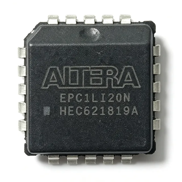
EPC1LI20N - 1Mb OTP FPGA Configuration PROM | Altera
EPC1LI20N

EPC1LI20N - 1Mb OTP FPGA Configuration PROM | Altera

The Altera (Intel) EPC1LI20N is a 1-Mbit one-time-programmable (OTP) configuration memory device designed to load SRAM-based Altera FPGAs at power-up, packaged in a 20-pin plastic J-lead chip carrier (PLCC). It operates from dual supply rails of 3.0 V to 3.6 V and 4.5 V to 5.5 V, supports an industrial temperature range of -40C to +85C, and is shipped in tubes. A configuration PROM is a non-volatile serial memory that stores the FPGA's bitstream and presents it to the FPGA's configuration controller on power-up. In the Altera taxonomy, the EPC1 family sits at the entry tier: a single-device, OTP solution for LUT-based FPGAs such as the Cyclone, FLEX 10K, and APEX families. EPC1 devices are programmed once with the Quartus / MAX+PLUS II software flow and then permanently drive nCONFIG, DCLK, and DATA0 lines during every subsequent FPGA configuration. Key specifications include a 1 Mb (1,048,576-bit) memory capacity, JTAG-compliant IEEE 1149.1 boundary-scan interface for in-system programming, a low-pin-count serial interface that minimizes FPGA pin usage during configuration, and programmable compression support that reduces configuration file size by 30-55%. The PLCC-20 footprint is the same J-lead package used across the entire EPC1 / EPC2 family, allowing board designers to migrate between OTP and flash-backed variants without PCB rework. The EPC1 architecture uses an internal oscillator and state machine to implement Altera's proprietary serial configuration protocol, automatically detecting the target FPGA density and clocking the bitstream without external glue logic. This makes it ideal for cost-sensitive, single-FPGA designs where board space and BOM count matter more than field-upgradability. Typical applications include factory-programmed FPGA configuration in industrial controllers, telecom line cards, and instrumentation where the bitstream is fixed for the product's lifetime. Engineers commonly pair the EPC1LI20N with Altera Cyclone II / III, FLEX 10KE, and ACEX 1K devices. When designing with the EPC1LI20N, note that the device is OTP - any bitstream revision requires physical replacement. Reserve the JTAG pins on the FPGA so the EPC1 can be programmed through the FPGA's JTAG chain in production. This page synthesizes distributor stock, parametric cross-references, and application guidance specific to the EPC1LI20N's 20-PLCC OTP configuration role - information not assembled in any single distributor listing.

USD $7.80 문의하기
EPC1LLC20 - 1Mb Serial Config Memory | Intel (Altera) | 20-Pin PLCC
EPC1LLC20

EPC1LLC20 - 1Mb Serial Config Memory | Intel (Altera) | 20-Pin PLCC

The Intel (formerly Altera) EPC1LLC20 is a 1-Mbit serial configuration memory device in a 20-pin Plastic Leaded Chip Carrier (PLCC) package, designed to store and stream configuration bitstreams to SRAM-based Altera FPGAs at power-up. It supports a serial configuration clock of up to 8 MHz and interfaces with Altera FLEX, ACEX, APEX, Cyclone, and Mercury device families via the dedicated serial configuration interface. A configuration memory (or configuration device) is a non-volatile storage IC that holds the FPGA bitstream so that the SRAM-based LUT fabric inside an FPGA can be re-loaded each time the system powers up, resets, or needs new logic. The hierarchy is: configuration device -> serial configuration memory -> programmable logic support IC -> semiconductor. Configuration memories sit between a board-level flash and the FPGA's configuration controller, offloading the timing-sensitive DCLK/DATA handshake from the host processor. Key features include 1,048,576 bits of flash storage, a 3.3V single-supply operation (2.7V to 3.6V tolerance), an industry-standard 4-pin serial interface (nCS, DCLK, DATA, nINIT_CONF/nCONFIG-compatible pinout), and 100,000 erase/program cycles endurance. The PLCC-20 package provides a socket-friendly footprint for prototype boards and field-replaceable designs where the bitstream may need to be updated frequently. EPC1LLC20 is fabricated on a 0.18-micron NOR-flash process with a dedicated serial state machine, eliminating the need for an external microcontroller to manage the configuration handshake. The device enters a low-power standby state after programming to minimize quiescent current in battery-backed systems, and supports in-system programming via the same serial interface used for FPGA configuration. Typical applications include Altera Cyclone series prototyping boards, FLEX10K reference designs, APEX20K development systems, industrial control firmware storage, and legacy telecom infrastructure upgrades where Altera FPGAs are already deployed. Designers often use the EPC1LLC20 alongside Altera ByteBlaster or USB-Blaster download cables for in-system reprogramming. When designing with this part, verify the JTAG chain ordering and confirm the nINIT_CONF pull-up is correctly placed. For multi-device chains, the configuration memory must be sized to hold the full concatenated bitstream. This page synthesizes distributor pricing, drop-in alternatives, and practical design notes not found in the original Altera datasheet.

견적 요청 문의하기
EPC1P18N - 1Mb Altera Config PROM for SRAM-based FPGAs
EPC1P18N

EPC1P18N - 1Mb Altera Config PROM for SRAM-based FPGAs

The Altera (Intel Programmable Solutions Group) EPC1P18N is a 1-Mbit one-time programmable (OTP) configuration memory device designed to store and load the configuration bitstream of SRAM-based Altera look-up-table (LUT) FPGAs such as the Cyclone, APEX, ACEX, and Mercury families. Housed in an 8-pin PDIP through-hole package, the EPC1P18N provides a simple, low-pin-count interface that streams bitstream data to the target FPGA at power-up through a dedicated serial configuration chain, eliminating the need for external boot memory in many designs. What is an FPGA configuration PROM? An FPGA configuration PROM (also called a configuration device or boot PROM) is a non-volatile serial memory that holds the FPGA's bitstream image and serially delivers it to the SRAM-based FPGA at power-up. Because SRAM is volatile, every time the FPGA powers on it must be re-loaded from an external source; the configuration PROM provides that source. The hierarchy is: FPGA configuration device -> configuration memory -> serial PROM -> non-volatile memory -> semiconductor memory. Altera configuration PROMs sit alongside the EPC2, EPC4, EPC8, and EPC16 in the same family, scaled by bitstream size. Key features include 1 Mbit of storage capacity (sufficient for legacy Cyclone-class bitstreams), dual supply support (3.0 V to 3.6 V and 4.5 V to 5.5 V) so the part can be paired with both 3.3 V and 5 V Altera FPGAs, Altera's proprietary serial configuration protocol, and industrial operating temperature range of -40 C to +85 C. The 8-pin PDIP package has a 0.300 inch (7.62 mm) row spacing and is supplied in tube packaging. In a typical system the EPC1P18N sits at the end of a daisy-chain of FPGA configuration devices driven by the FPGA's MSEL[2:0] configuration mode pins and the nCONFIG / nSTATUS handshake. Because the part is one-time programmable, bitstream updates require physical part replacement - the EPC1P18N is therefore not a field-upgradeable storage medium. Engineers designing new boards today typically choose a flash-based or controller-based configuration scheme, but the EPC1P18N remains in production for legacy board sustain and long-lifecycle industrial systems. Typical applications include legacy Altera Cyclone I boot memory, APEX 20K reference designs, ACEX 1K configuration storage, industrial control card bitstream retention, and 5 V-tolerant FPGA configuration rails. The dual-voltage support is the principal differentiator versus single-voltage competitors. When designing with the EPC1P18N ensure the target FPGA's configuration mode pins are set to select serial configuration from an EPC1-class device, and verify that the 1 Mbit capacity is sufficient for your compiled bitstream - oversize bitstreams require an EPC2 or larger.

견적 요청 문의하기
EPC1PC8 - 1Mb OTP Config PROM for FPGAs, 8-PDIP | Intel
EPC1PC8

EPC1PC8 - 1Mb OTP Config PROM for FPGAs, 8-PDIP | Intel

The Intel (formerly Altera) EPC1PC8 is a 1-Mbit one-time-programmable (OTP) Configuration PROM designed to configure SRAM-based Altera FPGA devices such as the ACEX 1K, APEX 20K (including 20KE and 20KC), FLEX 10K (including 10KE and 10KA), and FLEX 6000/A devices. Housed in an 8-pin plastic DIP (PDIP) through-hole package, the EPC1PC8 supports the Altera proprietary configuration scheme used by these legacy FPGAs and operates from a single 5V supply. It is the smallest density point in Altera's original EPC1 Configuration PROM family. What is a Configuration PROM? A Configuration PROM is a non-volatile memory device that stores the bitstream used to program a volatile-memory FPGA (such as SRAM-based LUT devices) every time the system powers up. The PROM sits on the FPGA's dedicated configuration pins (DATA0, DCLK, nCONFIG, nSTATUS, CONF_DONE) and serially shifts the configuration data into the FPGA. Because SRAM-based FPGAs lose their configuration when power is removed, the Configuration PROM is mandatory for any standalone boot - it transforms an otherwise volatile FPGA into a self-contained, deterministic system. Hierarchy: PROM -> Non-volatile memory -> Memory IC -> Semiconductor. Key features of the EPC1PC8 include 1,048,576 bits (1Mb) of one-time programmable storage, a 5V-only supply (VCC = 5.0V typical, with 3.3V or 5V I/O tolerance depending on FPGA), a simple 4-pin serial configuration interface (DATA, DCLK, nCS, OE), and support for Altera's proprietary serial configuration scheme. The 8-pin PDIP package is the industry-standard through-hole footprint (300 mil body, 2.54 mm pitch) used by classic logic and memory devices, simplifying hand prototyping, breadboard evaluation, and legacy system maintenance. The EPC1PC8 is internally organized to match the bitstream width and CRC scheme expected by its target FPGAs. Configuration is initiated by the host system pulling nCONFIG high on the FPGA; the FPGA then drives nSTATUS high and asserts OE on the PROM, which serially clocks out the bitstream on DCLK/Data. Because the part is OTP, the bitstream is written once during device programming (using a MasterBlaster, ByteBlaster, or compatible Altera programmer) and is retained for the life of the system without battery backup. Typical applications include configuring legacy Altera FLEX 10K and APEX 20K evaluation boards, industrial control retrofits that must remain bit-compatible with installed FPGA-based assets, and educational platforms teaching the fundamentals of FPGA boot flows. It is also used as a low-cost configuration source for designs where in-system reprogrammability is not required. When designing with the EPC1PC8, observe the recommended decoupling (0.1 uF ceramic close to VCC and a bulk 10 uF tantalum or aluminum cap), keep the DCLK trace short, and protect the OE/nCS lines from noise during configuration. Because the device is OTP, designers should program verified bitstreams and store a backup of the original .pof file. This page synthesizes distributor availability, drop-in compatible alternatives (including larger-density EPC family members and same-footprint cousins), and practical design notes not found in the original datasheet.

견적 요청 문의하기
EPC1PC8-NW - 1Mb OTP Configuration PROM 8-PDIP | Intel / Altera
EPC1PC8-NW

EPC1PC8-NW - 1Mb OTP Configuration PROM 8-PDIP | Intel / Altera

The Intel / Altera EPC1PC8-NW is a 1-Mbit one-time-programmable (OTP) serial configuration PROM designed to load configuration bitstreams into SRAM-based FPGAs such as the FLEX 10K, APEX 20K, Mercury, and Cyclone families. Housed in an 8-pin plastic DIP (PDIP) through-hole package with a 300-mil body, it stores up to 1,046,496 bits of configuration data and serially clocks the bitstream into the target FPGA on power-up via the DATA, DCLK, and nCONFIG interface. The -NW suffix indicates Pb-free (lead-free) matte-tin plating per JEDEC J-STD-020 MSL classification. A configuration PROM is a non-volatile serial memory that holds the FPGA's SRAM-based configuration image. Because SRAM LUT cells lose their configuration when power is removed, every FPGA power-up requires an external device to reload the bitstream. The EPC1 family reduces FPGA design complexity by integrating the configuration storage, address counter, oscillator (for older EPC1/EPC1441 devices), and tri-state DATA buffer in a single small package, eliminating the need for a separate boot ROM or microcontroller bootloader. Key features of the EPC1PC8-NW include a 3.3V or 5V core supply (VCC = 3.3 V to 5.0 V), a low-power CMOS process, an open-drain nSTATUS / CONF_DONE-compatible interface through the FPGA, automatic reset of the internal address counter when OE is driven low, and a JTAG-less simple serial interface (note: JTAG BST is supported only on the EPC2 family, not the EPC1). Programming is performed via the Altera ByteBlasterMV or BitBlaster download cable using the Quartus or MAX+PLUS II programmer flow. The architecture uses an on-chip ring oscillator (EPC1/EPC1441) or external clock (EPC2) to advance the internal address counter, sequentially presenting each bit on the DATA pin synchronous to DCLK from the FPGA. A low on OE resets the address counter and tri-states DATA, allowing multiple configuration sources to share a bus. The nCS pin enables the device output stage, supporting cascaded PROM chains for multi-device bitstream loading. Typical applications include boot configuration for Altera / Intel FPGAs in industrial controllers, telecom line cards, prototyping boards, and legacy MAX 7000 / FLEX 10K design refreshes. The wide VCC range and PDIP package also suit through-hole educational and breadboard designs where surface-mount configuration devices are impractical. When designing with the EPC1PC8-NW, place a 0.1 uF decoupling capacitor as close as possible to VCC (pin 8) and GND (pin 4), and verify the FPGA's MSEL pins select the appropriate configuration mode (AS or PS) for PROM interface compatibility. Designers migrating to newer Intel FPGA families should note that EPCS / EPCQ serial flash devices have largely replaced OTP PROMs in modern Cyclone IV / V / 10 designs. This page synthesizes drop-in alternatives (EPC1441PC8, EPC1LC20, EPC2LC20), pin-for-pin compatible parts, programming tool compatibility, and practical design notes not aggregated on a single distributor product page.

견적 요청 문의하기
EPC1PC8/PI8 - 1Mb OTP Configuration PROM, 8-PDIP | Altera
EPC1PC8/PI8

EPC1PC8/PI8 - 1Mb OTP Configuration PROM, 8-PDIP | Altera

The Altera EPC1PC8/PI8 is a 1-Mbit one-time-programmable (OTP) configuration PROM in an 8-pin PDIP package designed to store configuration bitstreams for SRAM-based Altera FPGAs including ACEX 1K, APEX 20K/20KC/20KE, APEX II, Arria GX, Cyclone, and Cyclone II families. It operates from 3.0 V to 3.6 V (3.3 V mode) or 4.75 V to 5.25 V (5 V mode) and supports a maximum configuration clock of 8 MHz in serial mode, enabling fast FPGA configuration at power-up. An OTP configuration PROM is a non-volatile memory device used to load the configuration bitstream into an SRAM-based FPGA each time the system powers up or reinitializes. Because SRAM-based FPGAs lose their configuration when power is removed, an external PROM (or other boot source) is required to reload the LUT and routing data on every power cycle. OTP devices are programmed once during board manufacture and provide a low-cost, simple boot path for production systems that do not need in-field reprogramming of the boot image. Key features of the EPC1PC8/PI8 include 1 Mbit of configuration storage, a serial configuration interface, an OE-driven address counter reset, an nCS chip-select control, cascading support for multi-device configuration chains, and compatibility with the Altera (now Intel) Quartus programming flow via the JTAG-style programming algorithm. The serial output data stream is clocked out to the FPGA's DATA0/DCLK pins until the entire bitstream has been delivered and the FPGA enters user mode. The device uses a simple four-wire serial interface (nCS, OE, DCLK, DATA) so the PCB footprint stays minimal and the BOM cost low. The 8-PDIP through-hole package supports hand-soldering, breadboard prototyping, and legacy industrial backplanes that still require DIP-form factor configuration memory, while a pin-compatible 8-pin SOIC variant (EPC1SI8) is offered for surface-mount designs. Typical applications include Altera/Intel Cyclone FPGA boot storage, APEX 20K industrial control configuration, ACEX 1K legacy board retrofits, prototyping platforms, and any production system that needs a deterministic one-time boot image loaded from a small serial PROM. The EPC1 family remains a cost-effective choice for designs that do not require in-system reprogramming of the boot PROM. When designing with the EPC1PC8/PI8, ensure that the OE line is driven low by the FPGA's CONF_DONE / nSTATUS logic to start the address counter, and that the nCS line is held in the correct state during FPGA configuration. Verify the FPGA's configuration clock maximum (typically 33 MHz for newer Cyclone families) versus the EPC1's 8 MHz ceiling, and use an EPCS or EPCQ device for higher clock rates. The 8-PDIP package is recommended for through-hole boards and prototyping; use the EPC1SI8 SOIC variant for surface-mount production. This page synthesizes distributor pricing, drop-in Altera and Intel alternatives, and practical configuration-design notes not found in the original datasheet, giving engineers a single reference for EPC1PC8/PI8 sourcing and design-in decisions.

견적 요청 문의하기
EPC1PC8CC - 1Mb FPGA Config PROM | Intel (Altera) | 8-Pin DIP
EPC1PC8CC

EPC1PC8CC - 1Mb FPGA Config PROM | Intel (Altera) | 8-Pin DIP

The Intel (formerly Altera) EPC1PC8CC is a 1-Mbit serial-configuration PROM designed to store configuration bitstreams for the ACEX 1K, APEX 20K, APEX II, ARRIA, Cyclone, Cyclone II, FLEX 10K, FLEX 6000, FLEX 8000, MAX 7000B/AE/S, MAX 9000, Mercury, Stratix, and Stratix II FPGA families. The device ships in an 8-pin PDIP plastic dual-in-line package (suffix PC8) and provides non-volatile, in-system serial configuration through a four-pin Altera serial configuration interface that includes nSTATUS, nCONFIG, DCLK, and DATA0 signals. A serial configuration PROM is a specialized non-volatile memory whose purpose is to boot an SRAM-based FPGA at power-up. Because SRAM FPGAs lose their configuration when power is removed, the PROM holds the bitstream image and serially clocks it into the FPGA's internal configuration RAM via the proprietary Altera Passive Serial (PS) mode. Within the power-management taxonomy, EPC1PC8CC sits at the boundary between Memory ICs and FPGA support components - a Configuration PROM is functionally a one-time-programmable (OTP) serial Flash memory that serves the FPGA boot function. Key features of the EPC1PC8CC include 1 Mb (1,048,576 bits) of configuration storage, a 17.6 Mb/s maximum DCLK configuration clock rate, automatic CRC error checking during bitstream transfer, an open-drain nSTATUS indicator pin, and a low-pin-count DIP-8 footprint that simplifies through-hole assembly for legacy and industrial designs. The device operates from a 3.3 V supply (VCC range 3.0 V to 3.6 V) and supports in-system programming via the JTAG chain when used with the Altera Quartus / Quartus Prime programmer. The internal array is organized as 1 Mb and uses EPROM technology, which is one-time-programmable but can be repeatedly read without wear. Altera's design allows the EPC1 to cascade with up to 16 additional EPC devices in a configuration chain via nCASC pin, although the PC8 package does not expose nCASC - only single-device configurations are supported in this footprint. Typical applications include FPGA configuration memory for industrial control boards, test and measurement instruments, prototyping platforms, communication line cards, and legacy Altera Cyclone/Stratix designs. The DIP-8 through-hole package makes the EPC1PC8CC particularly suitable for evaluation boards and breadboard-based prototypes where socketed, replaceable configuration memory is desired. The non-volatile, factory-programmed or JTAG-programmable nature of the configuration storage makes the EPC1PC8CC a one-time-programmable configuration source ideal for low-volume and production designs. When designing with this device, note that the EPC1PC8CC is one-time programmable; designers must verify the configuration image with Quartus programmer before committing the device. Designers should also account for an inrush current of up to 50 mA during configuration, and ensure that the upstream 3.3 V regulator can supply peak loads. The DIP-8 footprint cannot be cascaded - for multi-device configuration chains select the PLCC or TQFP variants of EPC1 or use EPC2. This page synthesizes XAIPART pricing tiers, drop-in EPC1 family alternatives that share the same DIP-8 footprint, and practical design notes not found in the original datasheet - a unique information gain that complements the manufacturer document and reduces design-in time for engineers maintaining legacy Altera-based boards.

견적 요청 문의하기
EPC1PC8CCD - 1Mb OTP Config PROM, 8-PDIP | Intel / Altera
EPC1PC8CCD

EPC1PC8CCD - 1Mb OTP Config PROM, 8-PDIP | Intel / Altera

The Intel / Altera EPC1PC8CCD is a 1-Mbit one-time-programmable (OTP) configuration memory device housed in an 8-pin plastic DIP (8-PDIP) through-hole package, designed to store and stream configuration bitstreams to Altera SRAM-based FPGAs and CPLDs at system power-up. It supports the legacy EPC1 (EPC1PC8) family interface and is supplied in the commercial 0C to +70C temperature range with a NiPdAu lead finish, designated by the "CCD" suffix meaning Commercial grade, DIP package, lead-free. A configuration PROM is a non-volatile memory device that holds the FPGA's programming bitstream and presents it to the target logic device through a serial configuration interface at every power-on or reconfiguration event. The EPC1 family is the second-generation Altera configuration PROM series, replacing earlier EPC1441/EPC1064 devices with higher density, lower power, and improved cascading. The device operates as a peripheral to the FPGA and is part of the broader FPGA configuration and programming hierarchy: configuration PROM -> non-volatile memory -> boot memory -> FPGA. Key features include 1 Mb (1,048,576 bits) of OTP storage, serial daisy-chain cascading to support multi-FPGA configurations or larger bitstreams, 3.3V core VCC operation, a low-power CMOS process, and a dedicated DATA output clock generated by the internal oscillator for handshaking with the Altera FLEX or APEX configuration controller. The 8-PDIP package provides easy insertion into sockets or through-hole prototyping boards, making the EPC1PC8CCD well suited to early design verification, low-volume production, and educational/development kits. From an architectural standpoint, the EPC1PC8CCD uses an anti-fuse OTP cell array programmed via the Altera programming hardware, with each bit accessed sequentially during FPGA configuration. The internal address counter increments on each rising edge of the internal configuration clock, and a CONF_DONE handshake with the FPGA ensures the bitstream has been fully delivered before the FPGA enters user mode. The device supports both single-device and multi-device (cascaded) configuration topologies. Typical applications include configuring Altera FLEX 6000 / FLEX 8000 / FLEX 10K, APEX 20K, and ACEX 1K family SRAM-based FPGAs, prototyping boards and lab development kits, industrial control systems using legacy Altera logic, and legacy board refreshes where the original EPC1PC8 bitstream must remain compatible. When designing with this device, engineers should note that OTP cells can be programmed only once, so designers must verify the bitstream is final before committing the configuration. The 8-PDIP package is intended for through-hole mounting and is not recommended for high-vibration surface-mount environments; for SMT designs, the equivalent EPC1PC8 in PLCC is preferred. This page synthesizes distributor pricing, drop-in same-package alternatives, and practical design notes not found in the manufacturer datasheet alone.

견적 요청 문의하기
EPC1PC8CEC - 1Mb OTP Configuration PROM, 8-PDIP | Intel / Altera
EPC1PC8CEC

EPC1PC8CEC - 1Mb OTP Configuration PROM, 8-PDIP | Intel / Altera

The Intel / Altera EPC1PC8CEC is a 1-Mbit one-time-programmable (OTP) serial configuration memory designed to load configuration data into SRAM-based FPGA devices such as the Altera FLEX 10K, APEX, ACEX, Cyclone, and MAX series on every power-up. Per the Altera Configuration Devices datasheet, the part stores up to 1,046,496 bits of configuration data (1046496x1 organization) in CMOS memory and is housed in an 8-pin PDIP (300-mil) through-hole package. A configuration PROM is a non-volatile serial memory that holds the FPGA bitstream so that an SRAM-based LUT device can be configured at every power-up, system reset, or remote reconfiguration event. Unlike flash-based FPGAs, SRAM LUTs lose their configuration when power is removed, so a separate boot PROM is mandatory for stand-alone or production systems. OTP PROMs replace older EPROM sockets and eliminate the in-system programming step. Key features of the EPC1PC8CEC include the standard Altera serial configuration interface (DATA, DCLK, nCONFIG, nSTATUS, CONF_DONE), 3.3V core supply, automatic CRC error detection, 8-pin PDIP through-hole package, and industrial operating temperature range. The device is cascadable for designs whose bitstream exceeds 1 Mbit (multiple EPC1 devices chain together via the nCASC pin). JTAG boundary-scan support is included for in-system verification. The EPC1PC8CEC uses a 4-pin serial interface (DATA, DCLK, nCONFIG, nSTATUS) originally defined for Altera's FLEX 8000/10K families and reused across ACEX, APEX, Cyclone, and later devices. Internally the part contains a CMOS UV-erasable cell array programmed at the factory; once programmed, the bitstream is permanent for the lifetime of the part. This makes the EPC1 family ideal for production volumes where field upgrades are not required. Typical applications include boot configuration for Altera Cyclone and MAX FPGAs in industrial controllers, prototype and production bitstream storage for FLEX 10K boards, retrofits of legacy designs that originally used UV EPROM sockets, and low-cost factory-programmed logic modules. Designers migrating to newer families should evaluate EPCQ, EPCQL, or the on-chip flash configuration of MAX II/MAX V before redesigning legacy boards. When designing with the EPC1PC8CEC, pay attention to the recommended 10 kohm pull-up resistor on nSTATUS and CONF_DONE, the decoupling requirement of 0.1 uF + 10 uF near VCC, and the trace-length matching of DCLK and DATA to avoid configuration failures on long backplanes. The suffix "CEC" denotes the commercial/industrial temperature grade and the 8-pin PDIP package option.

견적 요청 문의하기
EPC1PC8N - 1Mb Altera FPGA Config PROM, 8-PDIP | Intel
EPC1PC8N

EPC1PC8N - 1Mb Altera FPGA Config PROM, 8-PDIP | Intel

The Intel (formerly Altera) EPC1PC8N is a 1-Mbit serial configuration memory device designed for use with Altera FPGAs that lack built-in non-volatile storage. Housed in an 8-pin PDIP package, the EPC1PC8N provides a one-time-programmable (OTP) configuration data store for SRAM-based LUT devices such as members of the Altera Cyclone, APEX, and Mercury families. The part is the lead-free / RoHS-compliant "N" suffix variant of the legacy EPC1PC8. What is an FPGA configuration PROM? An FPGA configuration PROM (also called a serial configuration device) is a small serial Flash or EEPROM device whose sole purpose is to load the bitstream into a volatile SRAM-based FPGA at power-up. The hierarchy is: configuration PROM -> non-volatile memory -> serial memory -> semiconductor. Because most FPGAs are SRAM-based, they lose their configuration when power is removed; the configuration PROM acts as the boot source that re-loads the bitstream through a serial interface (typically Altera's PS or AS mode). Without a configuration PROM, the FPGA must be configured from a processor, Flash, or download cable at every power-up. Key features of the EPC1PC8N include 1,000,000 bits of OTP storage, a simple 4-wire serial interface to the host FPGA, low standby current, and 3.3V single-supply operation that matches Altera's standard I/O rails. The device is in-system programmable via the IEEE Std. 1149.1 JTAG interface, allowing boundary-scan testing and re-programming during board bring-up. From an architectural standpoint, the EPC1PC8N uses an internal oscillator to clock configuration data out to the FPGA in serial mode (DCLK + DATA). It is a write-once device using an anti-fuse cell that cannot be erased once programmed, which makes it well-suited to production environments where the bitstream is fixed. Typical applications include industrial control boards, telecom line cards, prototyping platforms, and any design that pairs a SRAM-based Altera FPGA with a stand-alone boot source. The 8-pin PDIP form factor is also convenient for development boards and through-hole educational kits. When designing with this device, observe the 3.3V VCC requirement and ensure the JTAG chain is correctly ordered so that the EPC1PC8N does not interfere with FPGA boundary-scan. Because the EPC1 is OTP, design engineers should verify the bitstream on a development kit before committing to production programming. This page synthesizes distributor stock and pricing, drop-in alternatives, and practical design notes that complement the manufacturer datasheet.

견적 요청 문의하기
EPC1PC8W - 1Mb OTP Configuration PROM for Altera FPGAs
EPC1PC8W

EPC1PC8W - 1Mb OTP Configuration PROM for Altera FPGAs

The Intel (formerly Altera) EPC1PC8W is a 1-Mbit one-time-programmable (OTP) configuration PROM designed to load configuration bitstreams into SRAM-based Altera/Intel FPGAs at power-up. Housed in an 8-pin PDIP package, the device stores the FPGA configuration image in non-volatile memory and serially shifts the data into the target FPGA through the standard Altera configuration interface (nCONFIG, nSTATUS, CONF_DONE, DATA0, DCLK). The EPC1PC8W is part of the EPC1 configuration device family that pairs with older Altera FLEX, ACEX, APEX, Cyclone and Stratix-class FPGAs. A Configuration PROM is a non-volatile serial memory that holds the FPGA's configuration bitstream. At system power-up, the FPGA's configuration controller reads the bitstream from the PROM through a synchronous serial interface (DATA, DCLK) and programs its internal SRAM-based configuration latches. Because SRAM-based FPGAs lose their configuration when power is removed, the configuration PROM acts as the boot memory that re-initializes the FPGA on every power cycle. The EPC1 family uses a dedicated Altera configuration protocol, not a generic SPI flash interface. Key features of the EPC1PC8W include 1,048,576 bits (1 Mb) of OTP storage, a simple 4-pin serial programming interface for in-system programming, 3.3V typical VCC operation with 5V-tolerant I/O, and cascadable support so multiple EPC1 devices can be chained to store larger bitstreams. Programming is one-time per cell: once an OTP bit is blown it cannot be erased, making the EPC1PC8W well suited to production volumes where the design has stabilized. The EPC1 architecture uses an industry-standard OTP memory cell array with on-chip address counters, a serial data engine, and Altera's proprietary configuration sequencer. Programming is performed by applying elevated VPP to the dedicated programming pin while toggling DCLK and shifting data on DATA0. Read-back during device verification uses the same pin set, allowing factory test of the programmed image before final assembly. Typical applications include boot memory for legacy Altera FLEX 10K, ACEX 1K, APEX 20K, Cyclone, Cyclone II, and Stratix FPGA designs. Designers use the EPC1PC8W in industrial controllers, telecom line cards, military/aerospace retrofits, and test equipment where the host board already targets the Altera configuration pinout and BOM does not allow a switch to a modern Cyclone V/10 or MAX 10 device. When designing with the EPC1PC8W, ensure the JTAG/programming header exposes nCONFIG, nSTATUS, CONF_DONE, DATA0, DCLK and that VCC decoupling follows the datasheet's 100 nF + 10 uF guidance. Because the part is OTP, verify the entire bitstream with the Quartus programmer before blowing the array in production.

견적 요청 문의하기
EPC1PCB - Altera Enhanced Config 1Mb Flash PLCC-20 | Intel
EPC1PCB

EPC1PCB - Altera Enhanced Config 1Mb Flash PLCC-20 | Intel

The Intel (Altera) EPC1PCB is an enhanced configuration device providing single-chip, high-speed configuration for SRAM-based FPGAs in a 20-pin Plastic Leaded Chip Carrier (PLCC-20) package. It integrates a configuration controller and flash memory on a single die, designed specifically for very-high-density LUT-based FPGA configuration data storage. The EPC1PCB supports FPGAs from the Altera APEX, FLEX, ACEX, Cyclone, and Stratix families with on-chip decompression and multi-volt I/O compatibility. A configuration device is a non-volatile memory IC that stores FPGA bitstream data and reloads it at every power-up, reset, or reconfiguration event because SRAM-based FPGAs lose their configuration when power is removed. Enhanced configuration devices add an internal configuration controller and a low-pin-count serial/parallel interface that emulates the behavior of a microprocessor-driven configuration sequence, freeing the FPGA's user I/O and reducing system complexity. Key features include a 1-megabit flash memory density, an internal oscillator that drives configuration timing without external components, support for FPP (Fast Passive Parallel) and PS (Passive Serial) configuration modes, and 3.3V VCC operation with 5.0V-tolerant I/O. The device re-programmability is in-system programmable via JTAG, eliminating the need for external programmers. Programming cycle endurance is rated for thousands of erase/program cycles. The architecture pairs a flash array with a state-machine controller that implements the Altera configuration protocol, including multi-device daisy-chaining via nCASC and nCS pins. Designers can configure a chain of multiple SRAM-based FPGAs from a single EPC1PCB by cascading additional configuration devices. The internal voltage translator allows the EPC1 to drive FPGAs with 1.5V, 1.8V, 2.5V, 3.3V, or 5.0V I/O banks directly from a 3.3V VCC supply. Typical applications include production configuration storage for APEX 20K, FLEX 10K, ACEX 1K, Cyclone, and Stratix FPGA designs in telecom, industrial control, and military/aerospace systems. The EPC1PCB is widely used in legacy Altera design flows where the bitstream must be retained across power cycles without a separate flash MCU. Multi-device configuration chains using nCASC/nCS pins support dense FPGA arrays that exceed a single device's capacity. When designing with the EPC1PCB, ensure the JTAG chain includes the EPC1 in the FPGA's boundary-scan order so in-system programming works correctly. The PLCC-20 socket allows field replacement without specialized tools, an advantage for legacy systems where the configuration device may need to be swapped to update bitstreams. Note that newer Cyclone/Stratix families prefer EPCQ or EPCQ-A serial configuration devices over the parallel EPC1 due to lower pin count and faster configuration time. This page synthesizes distributor availability, drop-in alternatives from the same EPC1 family, and practical design notes on JTAG chain order and nCASC multi-device configurations that are not consolidated in the manufacturer datasheet.

견적 요청 문의하기
EPC1PI8 - Altera 1Mb OTP Serial Config PROM | 8-PDIP
EPC1PI8

EPC1PI8 - Altera 1Mb OTP Serial Config PROM | 8-PDIP

The Altera EPC1PI8 is a 1-Mbit one-time-programmable (OTP) serial configuration PROM designed to store FPGA configuration bitstreams for Altera/Intel SRAM-based LUT devices such as ACEX 1K, APEX 20K, APEX II, Arria GX, Cyclone, Cyclone II, FLEX 10K, FLEX 6000, Mercury, Stratix, Stratix GX, Stratix II, and Stratix II GX. The device operates at up to 8 MHz configuration clock frequency, supports 5 V (4.5 V – 5.5 V) and 3.3 V (3.0 V – 3.6 V) supplies, and ships in an 8-pin PDIP through-hole package. Background: A configuration PROM is a non-volatile serial memory that holds the FPGA's bitstream so that an SRAM-based FPGA can be reconfigured at every power-up. The hierarchy is: configuration PROM -> serial configuration memory -> non-volatile memory -> programmable logic support IC. Unlike SPI flash or parallel boot PROMs, configuration PROMs use a dedicated FPGA configuration protocol (FPP, PS, or AS modes) and are optimized for short bitstreams with deterministic configuration time. EPC1-series PROMs are typically paired with older Altera FPGAs that pre-date modern EPCQ/QSPI flash boot solutions. Key features include 1 Mb of OTP storage, 8 MHz maximum DCLK frequency, a simple 4-wire serial interface (nCS, DCLK, DATA, OE), and dedicated FPGA-configuration timing. The device is one-time-programmable (not erasable), which suits production systems where the bitstream is finalized. EPC1PI8 supports both 3.3 V and 5 V VCC operation, allowing direct interface to 5 V-tolerant FPGA configuration pins. The EPC1 architecture uses a serial shift-register programming model with internal charge-pump generated programming voltages. Configuration data is clocked out LSB-first, MSB-first on a per-Altera-FPGA basis, and OE/nCS provide frame-level handshaking. Because the part is OTP, no UV window or in-system erase is possible - it is intended as the lowest-cost permanent configuration storage. Typical applications include legacy Altera/Intel FPGA configuration in industrial controllers, prototyping boards for Cyclone and APEX families, low-volume production systems, and as a second-source PROM in designs migrating from discontinued configuration devices. It is widely used on Altera/Intel development kits to demonstrate the configuration chain. When designing with EPC1PI8, observe the VCC ramp time and follow the Altera FPGA configuration handshake sequence exactly. Because EPC1PI8 is OTP, plan for a small number of pre-programmed parts during development; sample/engineering units should be ordered with known-good bitstreams. This page synthesizes distributor availability, lifecycle status, drop-in EPC1/EPC2 alternatives from the same Altera family, and practical design considerations not found in the original datasheet.

견적 요청 문의하기
EPC1PI8N - 1Mb OTP FPGA Config PROM, 8-PDIP | Altera / Intel
EPC1PI8N

EPC1PI8N - 1Mb OTP FPGA Config PROM, 8-PDIP | Altera / Intel

The Altera / Intel EPC1PI8N is a 1-Mbit one-time programmable (OTP) configuration PROM designed to store configuration bitstreams for Altera SRAM-based LUT FPGAs, housed in an 8-pin PDIP through-hole package. It supports dual supply operation at 3.0V-3.6V or 4.5V-5.5V and delivers factory-programmed configuration to FPGAs in the ACEX 1K, APEX 20K, APEX II, Arria GX, Cyclone, Cyclone II, FLEX 10K and Mercury families via a simple serial interface. What is an FPGA configuration PROM? An FPGA configuration PROM is a non-volatile memory that holds the FPGA's bitstream and loads it into the SRAM-based logic fabric at power-up. PROMs sit in the boot chain between a board-level storage source and the FPGA, occupying the same category as boot EEPROMs and flash-loader devices. As a member of the broader FPGA configuration memory family, it bridges firmware storage and volatile programmable logic, and is itself a sub-class of non-volatile serial memory in the memory IC hierarchy. Key differentiating features include 1-Mbit density, an industry-standard 4-pin serial interface (DATA, DCLK, nCS, OE), low-power CMOS technology and an operating temperature range of -40C to +85C. The 'N' suffix designates the standard 8-PDIP 0.300 inch through-hole package, and the 'I' indicates the industrial temperature grade. The EPC1PI8N is built on a CMOS OTP process, allowing one-time in-system or pre-programmed configuration. Programming is performed by Altera's Quartus / MAX+PLUS II toolchain with the Altera Programming Unit (APU) or third-party programmers that support the EPC1 instruction set. Typical applications include low-volume FPGA designs, factory-programmed industrial controllers, prototyping boards for legacy Altera FPGAs, and cost-sensitive embedded platforms that prefer a discrete configuration memory over a parallel flash plus controller. Its dual-voltage supply range allows direct interfacing to both 3.3V and 5V FPGA banks. Design trade-off: because the EPC1PI8N is OTP, any firmware update requires a physical device swap or socketed adapter. Designers who anticipate in-field firmware revision should consider JTAG-direct configuration, a flash-based equivalent, or a socketed DIP footprint.

견적 요청 문의하기
EPC1TC32 - Altera 1Mb FPGA Configuration PROM, 32-TQFP | Intel
EPC1TC32

EPC1TC32 - Altera 1Mb FPGA Configuration PROM, 32-TQFP | Intel

The Intel (formerly Altera) EPC1TC32 is a 1-Mbit serial-configuration PROM designed to configure SRAM-based LUT FPGAs such as the FLEX 10K, APEX, Mercury, ACEX 1K, and Cyclone families. Housed in a 32-pin Thin Quad Flat Pack (TQFP) measuring 7x7 mm, the EPC1TC32 stores the FPGA configuration bitstream and clocks it out via Altera's dedicated serial configuration interface during FPGA power-up. EPC1 devices are the original generation of Altera configuration PROMs, distinguished from the later EPCS serial flash family by their proprietary serial interface optimized specifically for Altera FPGA configuration streams. What is a configuration PROM? A configuration PROM is a non-volatile memory device whose sole purpose is to hold the FPGA bitstream and deliver it to the FPGA on every power-up. Unlike generic SPI flash, an FPGA configuration PROM is pre-validated by the FPGA vendor for the exact bitstream format, timing, and density required, eliminating the need to generate JIC/JIC files or manually program third-party flash. Configuration PROMs sit in the boot memory hierarchy alongside boot ROMs and boot flash, ensuring deterministic FPGA initialization before user logic begins executing. Key features include a 1 Mbit density, single-device configuration support for FLEX 10K and APEX families, and compatibility with Altera's proprietary serial configuration scheme. The device operates from a single 3.3V supply, supports in-system programming via the JTAG interface when used with an external controller, and uses Altera's standard 4-pin DATA/DCLK/nCONFIG/nSTATUS configuration bus. The TC suffix indicates commercial temperature grade (0C to +70C) and the 32-pin TQFP package. EPC1 devices cannot be cascaded and do not support ISP through their JTAG pins without additional external logic, a limitation addressed in the subsequent EPC2, EPC4, EPC8, and EPC16 enhanced devices. The EPC1 architecture is a one-time-programmable EPROM-based design with a serial shift-register output stage. Programming is performed by Altera programming hardware (e.g., the ByteBlasterMV or MasterBlaster download cable) using a programming algorithm that biases the device into programming mode. Once programmed, the contents are permanent and the device is dedicated to a single FPGA configuration. Modern equivalent solutions have largely moved to EPCS1/EPCS4 serial flash for new designs, but EPC1TC32 remains in service for legacy FLEX 10K and APEX board support and repair stock. Typical applications include legacy FLEX 10K configuration storage, APEX 20K configuration storage, ACEX 1K configuration storage, and Cyclone configuration on boards where original Altera PROMs are mandated. Industrial and military systems built around FLEX 10K FPGAs in the late 1990s continue to require EPC1-series PROMs for board-level rebuild and spare-part replacement. Modern Cyclone III/IV/V designs should use EPCS-series serial flash instead, which offers ISP and higher density. When designing with EPC1TC32, verify the FPGA family compatibility matrix - EPC1 supports only the original FLEX 10K, APEX, Mercury, ACEX 1K and Cyclone (original) families; it cannot configure Stratix, Cyclone II, or any newer family. The configuration interface timing must be observed: DCLK maximum is in the low-MHz range, and the nCONFIG/nSTATUS handshake must follow Altera's configuration sequence. This page synthesizes distributor availability, EPC1-family drop-in alternatives, and practical sourcing notes not found in the manufacturer datasheet, helping engineers locate pin-compatible configuration memory for legacy Altera FPGA boards.

견적 요청 문의하기