EPM240GT100I5N
EPM240GT100I5N - 240-LE MAX II CPLD, 4.7ns, 100-TQFP | Intel
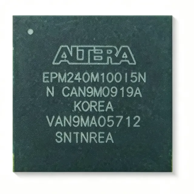
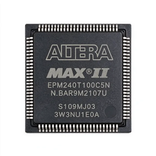
The Intel (Altera) EPM240GT100I5N is a MAX II family instant-on, non-volatile CPLD with 240 logic elements (192 macrocells), 4.7 ns pin-to-pin propagation delay, and 80 user I/Os in a 100-pin TQFP (14x14 mm, 0.5 mm pitch) package. Built on a 0.18-µm 6-layer-metal flash process, the device integrates 8 Kbits of non-volatile configuration Flash that eliminates the external configuration memory required by SRAM FPGAs, delivering true instant-on behavior at sub-100 µs power-up.
A CPLD (Complex Programmable Logic Device) is a non-volatile programmable logic device that sits in the hierarchy of glue logic between discrete 74-series logic gates, PALs/GALs, and SRAM FPGAs. CPLDs are favored for deterministic timing, predictable I/O behavior, fast input-to-output propagation, and instant-on capability, while FPGAs offer higher density but require configuration download at every power-up. The MAX II family specifically targets low-power, low-cost, instant-on logic integration for bus bridging, interface conversion, and power-up sequencing.
Key features include 4.7 ns tPD (speed grade -5), 304 MHz internal performance, in-system programmability through IEEE 1149.1 JTAG, MultiVolt core and I/O support allowing 1.5 V, 1.8 V, 2.5 V, 3.3 V interfaces on a single device, and an industrial temperature range of -40 °C to +100 °C. The 'I' in the part number designates the industrial temperature grade, and 'N' denotes a lead-free / RoHS-compliant finish. The MAX II architecture also provides 8 Kbits of user Flash memory that designers can use for parameter storage, board revision codes, or serial numbers.
The EPM240GT100I5N is implemented with a Logic Element (LE) fabric of 240 LEs organized into Logic Array Blocks (LABs) connected through a non-volatile interconnect, plus dedicated I/O registers at every pin. This LAB-based architecture delivers fixed propagation delay independent of routing density - a critical advantage over FPGAs for timing-sensitive applications such as address decoding, chip-select generation, and interrupt control.
Typical applications include I/O expansion and bus bridging in industrial controllers, glue logic and power-up sequencing in FPGA-based systems, peripheral interface glue in embedded computing boards, address decoding in legacy microcontroller systems, JTAG-controlled bootstrap logic, LED matrix driving, and field-reprogrammable control logic in telecommunications backplanes. Designers frequently select MAX II when instant-on behavior and deterministic timing outweigh the need for high logic density.
When designing with the EPM240GT100I5N, supply all four VCCINT and VCCIO bank pins even when migrating from a smaller density, because the EPM570 and EPM1270 in the same TQFP-100 footprint have more power pins that the EPM240 leaves floating. The JTAG chain shares TDO/TMS/TCK/TDI pins that must be brought out to a header or test point; pull-up on nCONFIG is recommended for reliable ISP. The Quartus II / Quartus Prime toolchain is used for design entry, synthesis, fitting, and programming.
This page synthesizes distributor pricing (DigiKey, Mouser, LCSC, Heisener), drop-in alternatives within the same MAX II family, and practical design notes not found on any single manufacturer page.
견적 요청
문의하기