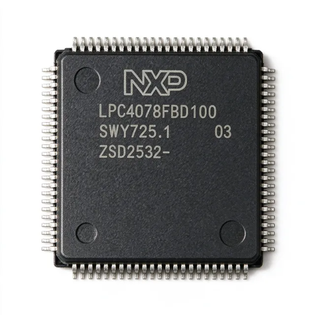
LPC2420FBD208K
LPC2420FBD208K - 72MHz ARM7 ROMless MCU | NXP | Ethernet
The NXP LPC2420FBD208K is a flashless 16-bit/32-bit ARM7 microcontroller with a 72 MHz Arm7TDMI-S CPU, Ethernet, CAN, USB 2.0, ISP/IAP, and an external memory interface, housed in a 208-pin LQFP package measuring 28 mm by 28 mm. It executes both 32-bit ARM and 16-bit Thumb instructions, allowing firmware developers to optimize code size and execution speed.
A microcontroller is a programmable semiconductor that integrates a CPU core, memory interfaces, communication peripherals, timers, and I/O control into one device. The LPC2420 belongs to the NXP LPC2400 family of embedded processors. Because this variant is ROMless, its application program must be stored in external memory and transferred through the external memory interface or programming path. This arrangement separates program storage from the MCU, supporting larger code, field-updateable firmware, or memory sharing.
The LPC2420's principal communication features include Ethernet, CAN, and USB 2.0 operating in device, host, and OTG roles. ISP/IAP support provides a practical path for programming and in-application firmware updates, while JTAG and embedded trace interfaces support real-time debugging. These capabilities make the device suitable for industrial gateways, USB-to-Ethernet bridges, embedded network controllers, service equipment, and data acquisition systems that need both wired networking and field maintenance.
The Arm7TDMI-S architecture supports deterministic embedded control while providing an established 16-bit/32-bit instruction set. A 72 MHz clock provides the execution rate for protocol handling, peripheral management, and control logic, while the external memory interface permits storage access beyond the device's internal program memory. The absence of integrated flash makes external boot memory, firmware loading, and board-level memory design central to the system architecture.
Typical implementations include Ethernet-connected industrial controllers, CAN-equipped machine controls, USB-to-serial or USB-to-network gateways, and embedded test systems. For each design, engineers must confirm the external memory device, bus timing, boot configuration, interrupt priorities, and communication isolation requirements. The manufacturer datasheet should also be used to establish the complete pin assignment, clock configuration, power requirements, and recommended decoupling network.
A key design consideration is that ROMless operation requires deliberate implementation of the boot and firmware chain. The external memory interface, reset behavior, and ISP/IAP pathway must work together reliably before application code is available. PCB design should preserve the package's 28 mm by 28 mm LQFP geometry, provide stable supply rails, route high-speed memory signals consistently, and keep switching or high-current circuitry away from sensitive clock and communication nodes.
This product record combines the verified 72 MHz ARM7 architecture, flashless configuration, communication peripherals, 208-LQFP mechanical format, and practical engineering guidance with sourced purchase information. It is intended to help designers evaluate interface coverage, memory architecture, debug access, package constraints, and system-level integration before committing an LPC2400-series design to hardware.
견적 요청
문의하기