제품 (19,000+)

EFM32ZG210F8-B-QFN32 - 24MHz 8KB Cortex-M0+ MCU | Silicon Labs
EFM32ZG210F8-B-QFN32

EFM32ZG210F8-B-QFN32 - 24MHz 8KB Cortex-M0+ MCU | Silicon Labs

The Silicon Labs EFM32ZG210F8-B-QFN32 is a 24 MHz ARM Cortex-M0+ Zero Gecko microcontroller with 8 KB of Flash memory, 2 KB of RAM, and 24 digital I/O pins in a 32-QFN 6 x 6 mm package. It combines a low-power embedded platform with 2 x 16-bit timers and operates from a 1.98 V to 3.8 V supply range. A microcontroller is a programmable system-on-chip that integrates a processor core, memory, and peripherals into one package. The EFM32 Zero Gecko family belongs to the hierarchy of 32-bit microcontroller, embedded processor, and low-power semiconductor devices. The ARM Cortex-M0+ architecture provides a compact instruction set suited to control-intensive systems that prioritize energy efficiency, predictable response, and low system complexity. Key features include a maximum operating frequency of 24 MHz, 8 KB Flash, and 2 KB RAM. Silicon Labs specifies run-mode consumption as low as 114 uA/MHz and stop-mode consumption as low as 0.5 uA. The device also provides autonomous peripherals, analog integration, energy-saving modes, and fast wake-up behavior. These characteristics make it useful where the controller must monitor sensors, update outputs, and remain available for infrequent communication without continuously loading a battery. The EFM32ZG210F8-B-QFN32 is based on the 32-bit ARM Cortex-M0+ processor and provides 24 digital I/O pins for external sensing, switching, and control functions. Its 2 x 16-bit timers support periodic timing and event generation. The integrated analog and peripheral resources reduce the need for external components in compact sensing and energy-harvesting products. Typical applications include smart energy meters, water and gas meters, industrial sensor nodes, wearable devices, and low-power IoT equipment. In these systems, the 8 KB Flash capacity suits compact firmware, while the 2 KB RAM allows moderate protocol buffering and peripheral management without requiring a larger microcontroller. Designers should follow Silicon Labs hardware guidance in application note AN0002, EFM32 Hardware Design Considerations. In particular, the AVDD_x, VDD_DREG, and IOVDD_x pins must be connected together at the PCB level, with an optional filter, and supply decoupling should follow the manufacturer reference layout. This page combines manufacturer specifications, distributor availability references, same-package Zero Gecko options, and practical hardware-design notes to support part selection and PCB planning beyond a distributor listing alone.

견적 요청 문의하기
EFM32ZG210F8-QFN32 - 24MHz Cortex-M0+ MCU | Silicon Labs
EFM32ZG210F8-QFN32

EFM32ZG210F8-QFN32 - 24MHz Cortex-M0+ MCU | Silicon Labs

The Silicon Labs EFM32ZG210F8-QFN32 is a 32-bit ARM Cortex-M0+ microcontroller operating up to 24 MHz, with 8 kB of Flash memory, 2 kB of RAM, and 24 digital I/O pins in a 32-QFN 6 x 6 mm package. It belongs to the EFM32 Zero Gecko family and combines a compact embedded processing core with low-power operating modes for energy-sensitive embedded systems. An ARM Cortex-M0+ microcontroller is a reduced-instruction-set embedded processor used to monitor sensors, process control signals, and manage system peripherals. The Cortex-M0+ architecture belongs to the broader microcontroller and embedded-processing hierarchy, while the EFM32 Zero Gecko family adds energy-saving features, fast wake-up behavior, autonomous peripherals, and integrated analog functions for compact control designs. The EFM32ZG210F8-QFN32 provides 8 kB of Flash, 2 kB of RAM, 24 digital I/O pins, and two 16-bit timers. Its 24 MHz maximum operating speed supports responsive control tasks while the device can consume as little as 0.5 uA in Stop mode and 114 uA/MHz in Run mode, according to the Silicon Labs EFM32ZG datasheet. These figures make the MCU suitable for systems where average power consumption is more important than sustained processing throughput. The Zero Gecko platform emphasizes low-energy operation rather than high-performance computation. Its sleep and stop behavior allows firmware to remain responsive to selected events while reducing energy use between measurements. The EFM32 implementation also includes a Wake-up Interrupt Controller for managing interrupts that occur while the CPU is asleep, supporting duty-cycled sensing and control systems that must promptly resume computation. Typical uses include battery-powered energy and gas meters, smart water meters, compact environmental sensors, industrial monitoring nodes, and other embedded systems that periodically acquire data and transmit or display results. The 32-QFN package supports high-density placement on compact boards, while the 24 I/O pins provide connections for digital inputs, outputs, serial interfaces, and external sensing hardware. Designers should account for the limited 8 kB Flash and 2 kB RAM when planning firmware, boot code, diagnostics, and communication buffers. The manufacturer datasheet directs PCB designers to the “AN0002 EFM32 Hardware Design Considerations” application note for board-layout guidance, including decoupling and exposed-pad implementation. This page consolidates verified manufacturer specifications, distributor references, same-family drop-in candidates, package details, and practical design guidance. It is intended to help engineers evaluate the EFM32ZG210F8-QFN32 for compact, low-power embedded designs without substituting unsupported specifications.

견적 요청 문의하기
EFM32ZG222F16-QFP48 - 24MHz 16KB MCU | Silicon Labs
EFM32ZG222F16-QFP48

EFM32ZG222F16-QFP48 - 24MHz 16KB MCU | Silicon Labs

Silicon Labs EFM32ZG222F16-QFP48 is a 32-bit ARM Cortex-M0+ Zero Gecko microcontroller rated for operation up to 24 MHz, with 16 kB of Flash memory, 4 kB of RAM, 37 digital I/O pins, and two 16-bit timers in a 48-pin TQFP package measuring 7 x 7 mm. It is designed for energy-sensitive embedded systems that require efficient processing, low-power operation, fast wake-up behavior, and energy-saving modes. The device supports 2.5 V and 3.3 V supply configurations according to the verified product data. A microcontroller is a programmable system-on-chip that integrates a processor core, nonvolatile program memory, working RAM, and peripherals into one compact package. The ARM Cortex-M0+ architecture belongs to the embedded processor hierarchy and is commonly used for control-oriented products requiring deterministic operation and efficient code execution. Within the EFM32 product family, the Zero Gecko platform emphasizes low-power sensing and control rather than high-performance compute. The EFM32ZG222F16-QFP48 combines a 24 MHz Cortex-M0+ core with 16 kB Flash and 4 kB RAM. Its 37 digital I/O pins provide connections for sensors, indicators, actuators, and control signals. Two 16-bit timers support periodic timing, event counting, and basic control-loop tasks. The manufacturer describes the platform as incorporating low-energy techniques, fast wake-up times, and energy-saving modes for battery-powered and other energy-conscious equipment. The device family also emphasizes autonomous peripherals, analog integration, and low power consumption. According to the Silicon Labs Zero Gecko datasheet, Zero Gecko devices can consume as little as 0.5 microamp in Stop mode and 114 microamps per megahertz in Run mode. These figures make the MCU suitable for systems that spend substantial time between infrequent user interactions or sensor events and must maintain a low average power budget. Typical uses include connected utility meters, water and gas monitoring, industrial sensing nodes, compact environmental monitors, and low-power embedded controls. In these systems, the Cortex-M0+ processor handles local logic while the integrated timers and digital I/O manage periodic sampling, status indicators, and external interfaces. Battery operation benefits from the documented Stop and Run current characteristics, although the final battery life depends on the complete firmware duty cycle, sensor load, and supply circuitry. Designers should verify the exact pin multiplexing, peripheral assignments, and board requirements against the manufacturer datasheet before layout. Decoupling, grounding, programming access, clock configuration, and unused-pin treatment are especially important in a 48-pin mixed-signal embedded design. The supplied web evidence does not include a complete 48-pin assignment, so this page does not reproduce an inferred pinout or fabricate individual signal names. This page consolidates the verified manufacturer and distributor data into an application-oriented overview of the EFM32ZG222F16-QFP48. It also separates confirmed memory, speed, package, and low-power characteristics from unverified attributes and explains why fewer drop-in alternatives are listed than normally required. Engineers can use the comparison table, practical design notes, and sourcing questions to evaluate the MCU without mistaking incomplete public snippets for complete datasheet coverage.

견적 요청 문의하기
EFM32ZG222F32-QFP48 - 24 MHz Cortex-M0+ 32KB MCU | Silicon Labs
EFM32ZG222F32-QFP48

EFM32ZG222F32-QFP48 - 24 MHz Cortex-M0+ 32KB MCU | Silicon Labs

The Silicon Labs EFM32ZG222F32-QFP48 is an ARM Cortex-M0+ Zero Gecko microcontroller operating up to 24 MHz, with 32 kB of Flash memory, 4 kB of RAM, and 37 digital I/O pins in a 48-TQFP 7 x 7 mm package. It is designed for energy-sensitive embedded systems that need low-power operation, fast wake-up behavior, and autonomous peripheral operation without relying on an active CPU loop. A microcontroller is a programmable semiconductor that integrates a processor core, memory, and peripherals such as GPIO, timers, communications interfaces, and analog blocks. The EFM32ZG Zero Gecko family combines a 32-bit ARM Cortex-M0+ processor with Silicon Labs low-energy techniques. This positions the device within the hierarchy of embedded controller, microcontroller, 32-bit microcontroller, ARM Cortex microcontroller, and power-management-oriented embedded processing. The verified device data identifies 24 MHz operating speed, 32 kB Flash, 4 kB RAM, 37 digital I/O pins, and two 16-bit timers. The EFM32ZG family data also reports consumption as low as 0.5 uA in Stop mode and 114 uA/MHz in Run mode. Autonomous peripherals allow supported timer, ADC, and communication activity to continue while the processor sleeps, reducing the energy cost of periodic sensing and control tasks. Supply voltage is specified as 1.98 V to 3.8 V, supporting both 2 V and 3.3 V powered systems. The integrated analog and communications resources make the device applicable to industrial control, energy measurement, smart metering, connected sensing, and low-power embedded products. Battery-operated designs benefit from fast wake-up behavior and energy-saving modes that reduce unnecessary processor activity. Engineering trade-offs include a modest 4 kB SRAM budget for protocol buffering and application data, and a Cortex-M0+ core intended for compact control workloads rather than heavy graphics or complex digital signal processing. Board designs should provide the voltage range required by the device and verify decoupling, clock, debug, and exposed-pin requirements against the manufacturer datasheet. This page combines manufacturer specifications, distributor availability, power characteristics, package details, and practical replacement analysis. It also distinguishes a verified same-footprint option from reel packaging variants and cross-family parts that are not automatically pin-to-pin compatible.

견적 요청 문의하기
EFM32ZG222F4-QFP48 - 24MHz Cortex-M0+ MCU | Silicon Labs
EFM32ZG222F4-QFP48

EFM32ZG222F4-QFP48 - 24MHz Cortex-M0+ MCU | Silicon Labs

Silicon Labs EFM32ZG222F4-QFP48 is a 32-bit ARM Cortex-M0+ microcontroller operating up to 24 MHz, with 4 kB Flash, 2 kB RAM, and 37 digital I/O pins in a 48-pin TQFP (7 x 7 mm) package. It belongs to the Zero Gecko family and is designed for energy-sensitive embedded systems that require low-power operation, rapid wake-up, and compact code footprint. A microcontroller is an integrated circuit that combines a processor core, memory, peripherals, and I/O in one device. In the device hierarchy, the EFM32ZG222F4-QFP48 is a microcontroller, or MCU, within the broader category of embedded semiconductors. Its ARM Cortex-M0+ core supports compact, deterministic control tasks, while the Zero Gecko low-energy platform makes it suitable for systems that spend much of their operating time in low-power states. Key features include a maximum clock frequency of 24 MHz, 4 kB of Flash, 2 kB of RAM, and two 16-bit timers. The device also provides 37 digital I/O pins in its 48-lead package. Its low-power platform includes energy-saving modes and fast wake-up behavior, helping battery-operated products reduce the amount of time spent consuming power. The manufacturer documentation also identifies AES capability and an ADC in product-level descriptions. The EFM32ZG222 family combines an ARM Cortex-M0+ processor with low-power system features and a peripheral set intended for embedded control. Its small 4 kB Flash capacity favors compact firmware rather than GUI-heavy or connectivity-intensive applications. The 48-pin TQFP package provides substantially more I/O than smaller 20-pin or 32-pin devices, making it useful when external sensors, switches, indicators, or interface circuits require dedicated pins. Typical applications include low-power sensor nodes, connected accessories, compact industrial controllers, building-automation endpoints, portable measurement equipment, and consumer accessories. The combination of 24 MHz processing speed, 37 digital I/O pins, and low-energy modes supports periodic sensing, local control, and short communication transactions without requiring a higher-power MCU. When designing around this device, engineers should verify the exact peripheral pin assignments and electrical limits in the EFM32ZG222 datasheet. Decoupling, programming access, clock configuration, and low-power state transitions must be handled according to the manufacturer reference design; the 4 kB Flash and 2 kB RAM limits also require firmware-size budgeting before feature commitments. This product record combines manufacturer specifications, distributor availability, cross-reference evidence, and engineering-focused application guidance. It also distinguishes verified drop-in alternatives from options whose memory capacity or ordering code differs, helping designers make a replacement decision without relying on package similarity alone.

견적 요청 문의하기
EFM32ZG222F8-QFP48 - 24MHz 8KB Flash MCU | Silicon Labs
EFM32ZG222F8-QFP48

EFM32ZG222F8-QFP48 - 24MHz 8KB Flash MCU | Silicon Labs

The Silicon Labs EFM32ZG222F8-QFP48 is an ARM Cortex-M0+ Zero Gecko microcontroller with a 24 MHz maximum clock, 8 KB Flash memory, 2 KB RAM, and 37 digital I/O pins in a 48-pin TQFP package. It is designed for energy-sensitive embedded systems that require a compact 32-bit controller, low-power operation, and rapid wake-up behavior. A microcontroller is an embedded semiconductor that integrates a CPU core, program memory, data memory, peripherals, and I/O into one device. The EFM32 Zero Gecko family belongs to the 32-bit microcontroller -> embedded processor -> semiconductor hierarchy. Its ARM Cortex-M0+ core provides a compact instruction set and event-driven execution, while the low-energy architecture supports duty-cycled products in which the MCU spends most of its time asleep. The verified device data identifies a 24 MHz operating speed, 8 KB Flash organized as 8K x 8, 2 KB RAM, and two 16-bit timers. The manufacturer describes fast wake-up times and energy-saving modes as core platform features. A 1.98 V to 3.8 V supply range appears in the alternatives cross-reference data, and the package is a 48-pin TQFP measuring 7 x 7 mm. The 37 digital I/O pins provide connections for sensors, actuators, communications, and user controls. This MCU is suitable for compact industrial sensing, connected sensor nodes, building controls, portable instruments, and low-power embedded products. Its small memory footprint favors focused control tasks rather than complex graphical interfaces or large application workloads. The 48-pin TQFP also exposes more I/O than the smallest packages while remaining compatible with conventional leaded assembly processes. Designers should verify the exact peripheral pin assignments, programming interface, and operating-mode limits against the manufacturer datasheet before layout release. Decoupling, ground-return planning, and separation between analog and digital circuitry remain important when the MCU drives sensors or communication modules. This page combines verified manufacturer and distributor information with practical selection guidance, application context, and compatibility-focused alternative research. It is designed to help engineers evaluate the EFM32ZG222F8-QFP48 faster while retaining traceability to the supplied product data.

견적 요청 문의하기
EFM8BB21F16G-C-QFN20R - 50MHz 16KB 8-Bit MCU | Silicon Labs
EFM8BB21F16G-C-QFN20R

EFM8BB21F16G-C-QFN20R - 50MHz 16KB 8-Bit MCU | Silicon Labs

Silicon Labs EFM8BB21F16G-C-QFN20R is an 8-bit EFM8 Busy Bee microcontroller with a 50 MHz CIP-51 core, 16 KB of Flash memory, and a 20-QFN 3x3 mm package. The verified distributor listing identifies 16 digital I/O and 2.5 V/3.3 V operation, while the related Mouser result confirms 2.25 KB RAM. Its compact package and integrated analog peripherals suit space-constrained embedded systems. An 8-bit microcontroller is a programmable semiconductor containing a CPU core, memory, digital I/O, timers, and peripherals on one integrated circuit. The EFM8 Busy Bee family combines an 8051-compatible architecture with enhanced peripherals, allowing compact embedded controllers to execute control logic, sample analog signals, and manage communications without requiring separate components. This MCU therefore sits between a basic microcontroller and a more complex mixed-signal embedded controller. The verified data highlights a 50 MHz operating speed, 16 KB Flash, 2.25 KB RAM, 16 digital I/O lines, and a 3x3 mm QFN-20 package. Related Silicon Labs family information lists a 12-bit ADC, analog comparators, programmable counter array channels, and additional communication peripherals. These integrated resources reduce board area and simplify designs requiring sensor acquisition, timing, or low-speed communication. The C-QFN20R ordering suffix identifies a packaged 20-QFN tape-and-reel configuration; the provided data does not independently establish every electrical limit for this exact suffix. The family datasheet should be used for package dimensions, pin functions, electrical characteristics, clocking, memory behavior, and programming details. Because the MCU integrates both digital and analog functions, careful grounding and short analog traces remain important. Typical uses include compact sensor controllers, consumer-electronics accessories, motor-control or timing subsystems, medical-device control boards, and industrial automation modules. The 20-QFN package reduces footprint compared with larger leaded packages, but exposed-pad thermal management and assembly process controls must be considered. The 50 MHz core provides useful headroom when coordinating peripheral activity and control tasks. For PCB design, use the manufacturer datasheet and reference-manual pin definitions rather than assuming package-side numbering. Place decoupling capacitors close to supply pins, provide a clean analog reference and ground arrangement, and verify exposed-pad copper against the package drawing. Confirm programming, clock, reset, and boot requirements before committing the layout. This page combines verified distributor and manufacturer information with application guidance, datasheet links, and a cautious replacement analysis. Because exact electrical and lifecycle fields were not supplied in the source data, they are marked as needed instead of being inferred. That approach keeps purchasing and design decisions traceable to verifiable EFM8BB2 documentation.

견적 요청 문의하기
EFM8BB21F16I-C-QSOP24 - 50MHz 8051 MCU, 16KB Flash, QSOP-24 | Silicon Labs
EFM8BB21F16I-C-QSOP24

EFM8BB21F16I-C-QSOP24 - 50MHz 8051 MCU, 16KB Flash, QSOP-24 | Silicon Labs

The Silicon Labs EFM8BB21F16I-C-QSOP24 is an 8-bit CIP-51 8051-core microcontroller from the Busy Bee 2 (EFM8BB2) family, operating at up to 50 MHz with 16 KB of Flash and 2.25 KB of RAM in a 24-pin QSOP package. It integrates a 12-bit ADC, enhanced PWM, and precision analog peripherals in a compact surface-mount footprint designed for space-constrained embedded designs. The industrial-grade device operates from a 2.2 V to 3.6 V supply across -40 to +125 C. A microcontroller (MCU) is a single-chip computer containing a processor core, program and data memory, and a set of programmable I/O and peripheral interfaces. The 8051 architecture, introduced by Intel in 1980 and still widely used today, is a CISC 8-bit core with an instruction set optimised for bit-level control and small-form-factor embedded code. Silicon Labs' EFM8 Busy Bee line modernises this core with a single-cycle CIP-51 implementation, integrated high-precision analog, and a low-power platform aimed at industrial, consumer, and embedded-control applications. Key features include a 50 MHz single-cycle 8051 core delivering ~50 MIPS, 16 KB in-system programmable flash, 2.25 KB RAM, a 12-bit 200 ksps ADC, multiple timers (5 x 16-bit), a 3-channel PCA for PWM/capture, I2C/SPI/UART communication peripherals, and on-chip temperature sensor. The 24-pin QSOP package supports up to 21 digital I/O pins in a small 8.7 mm x 3.9 mm footprint suitable for high-density PCB designs. Typical applications include industrial sensor interfaces, LED lighting controllers, motor-control signal conditioning, capacitive-touch front panels, and consumer peripherals. The wide -40 to +125 C operating range and AEC-Q100 readiness on related family members also suit the device for automotive body and HVAC subsystems when used with automotive-graded siblings. When designing with the EFM8BB21F16I-C-QSOP24, ensure the supply rail is decoupled with at least a 1 uF bulk and 100 nF ceramic capacitor pair placed close to the VDD pin. The device has no internal regulator; the supply must remain within 2.2 V-3.6 V at all times including transients. Use Simplicity Studio for configuration, flashing, and energy profiling during development. This page synthesizes distributor pricing, drop-in alternatives, and practical design notes not found in the manufacturer datasheet.

견적 요청 문의하기
EFM8BB51F16G-C-QFN20R - 50MHz 16KB 8051 MCU | Silicon Labs
EFM8BB51F16G-C-QFN20R

EFM8BB51F16G-C-QFN20R - 50MHz 16KB 8051 MCU | Silicon Labs

Silicon Labs EFM8BB51F16G-C-QFN20R is an 8-bit CIP-51 8051 Busy Bee microcontroller operating at 50 MHz, with 16 kB Flash, 1.28 kB RAM, and 16 GPIO in a 20-QFN 3 x 3 mm package. It is designed for compact embedded control applications requiring efficient 8051 processing, integrated flash memory, and a broad set of peripherals. An 8-bit microcontroller such as the EFM8BB51F16G-C-QFN20R is a programmable semiconductor that executes firmware, reads inputs, controls outputs, and manages communication or timing functions within a larger embedded system. The EFM8 Busy Bee family belongs to the broader 8-bit MCU and embedded-processing hierarchy, making it suitable for control-centric products where cost, compactness, and deterministic peripheral integration matter more than high-end processing performance. The device provides 4 x 16-bit timers and 3 PCA channels according to the manufacturer product information. Its 50 MHz operating frequency supports efficient execution of typical control logic, while 16 kB Flash stores firmware and 1.28 kB RAM supports working data. The 16 GPIO provide connections for sensors, switches, actuators, indicators, and other embedded-system signals within the 3 x 3 mm QFN-20 footprint. The EFM8BB51 family uses the wide-supply 5 V Busy Bee platform and is specified for operation from -40 °C to 85 °C. The supplied manufacturer page identifies additional communication peripherals, although the exact peripheral inventory is not enumerated in the verified web data. Applications include compact sensor controllers, industrial monitoring modules, building-control interfaces, communication equipment, and low-cost consumer devices. The principal design consideration is package and firmware compatibility. EFM8BB51F16G-C-QFN20R must be placed on a PCB footprint matching the 20-QFN 3 x 3 mm package, with careful attention to exposed-pad layout, power routing, decoupling, and signal integrity. The manufacturer EFM8BB51 datasheet should be used as the authoritative source for pin assignments, electrical limits, startup behavior, and programming details. This product page consolidates verified distributor specifications, manufacturer documentation, package information, sourcing context, and practical design guidance. Availability and pricing should be checked against current distributor records, while lifecycle and exact alternate-device suitability should be confirmed before production release.

견적 요청 문의하기
EFM8LB11F32ES1-C-QFN24R - 8-bit 72MHz Laser Bee MCU, 32KB Flash | Silicon Labs
EFM8LB11F32ES1-C-QFN24R

EFM8LB11F32ES1-C-QFN24R - 8-bit 72MHz Laser Bee MCU, 32KB Flash | Silicon Labs

The Silicon Labs EFM8LB11F32ES1-C-QFN24R is a CIP-51 8051-core "Laser Bee" 8-bit microcontroller running at 72 MHz with 32 KB flash and 2.25 KB RAM in a 24-pin QFN (3x3 mm) package. It is supplied on a 3.3 V typical rail (2.2 V to 3.6 V) and integrates a 14-bit ADC, two 12-bit DACs, a 4-channel PWM, and the standard EFM8 peripheral set including I2C, SPI, and UART. Laser Bee is Silicon Labs' high-throughput 8-bit MCU family that retains the classic 8051 instruction set while pushing the core to a 72 MHz pipeline, achieving roughly 50 MIPS effective throughput. In the broader taxonomy, EFM8LB1 sits under 8-bit microcontrollers, which are themselves a sub-category of microcontrollers (MCU), embedded controllers, and finally integrated circuits (IC). Compared with older 8051 parts (typically 12 MHz, 1 MIPS/MHz), the Laser Bee core delivers 7-8x higher compute density, making it suitable where determinism of the 8051 is preferred but throughput of an ARM Cortex-M0+ is not required. The device integrates 32 KB single-cycle flash, 2.25 KB RAM, 13 digital I/O (20 per the supplier listing) plus analog, an internal 49 MHz ±2% HFO, and a hardware cryptographic accelerator is not included at this family tier. Peripherals visible from the part number suffix ("S1") include UART, SMBus/I2C, SPI, PCA, timers, and a 14-bit 12-channel SAR ADC. The "C" in the suffix indicates revision C silicon, which improves ADC linearity and lowers active current compared with revision A/B parts. Architecturally, the Laser Bee core is a single-cycle 8051 with branch prediction and a tightly-coupled flash controller; this avoids the multi-cycle fetch penalty of legacy 8051s. The internal 49 MHz HFO can drive the core directly or be divided, and a low-frequency 32 kHz oscillator backs RTC-mode sleep. The 14-bit ADC at 900 ksps and two 12-bit DACs provide direct analog I/O for sensor conditioning loops without external converters. Typical applications include BLDC motor control (FOC sensorless), USB-C power delivery (PD) negotiation, portable medical sensor read-out, and lighting-control modules requiring up to 20 PWM channels. This part also fits general-purpose 8051 socket upgrades in industrial HMI and HVAC controllers where the existing firmware stack must be preserved. When designing with this part, route the QFN-24 exposed pad (pin 25 / DAP) directly to a contiguous ground pour - this is the primary thermal and electrical return path. Keep ADC traces short and symmetric, and use a separate analog supply decoupling node if mixed-signal accuracy matters. This page synthesizes distributor pricing, drop-in same-package alternatives, and design considerations not found in the manufacturer datasheet.

견적 요청 문의하기
EFM8LB12F64E-C-QFN24 - 72MHz 8051 MCU 64KB Flash QFN-24 | Silicon Labs
EFM8LB12F64E-C-QFN24

EFM8LB12F64E-C-QFN24 - 72MHz 8051 MCU 64KB Flash QFN-24 | Silicon Labs

The Silicon Labs EFM8LB12F64E-C-QFN24 is a CIP-51 8051-core 8-bit microcontroller from the Laser Bee EFM8LB1 family, delivering 72 MHz CPU performance with 64 KB Flash, 4.25 KB RAM, and a high-integration analog peripheral set, housed in a 24-pin QFN (3x3 mm) package. It integrates a 14-bit 12-channel ADC capable of up to 900 ksps, four 12-bit DACs, two low-current comparators, and four configurable logic units, providing an analog-rich MCU for optical modules and precision sensing. An 8-bit microcontroller (MCU) such as this EFM8LB1 device is a single-chip computer that combines an 8051-compatible CPU core, Flash program memory, RAM, and a rich set of analog and digital peripherals. Within the broader semiconductor taxonomy, an MCU falls under microcontrollers, which in turn sit inside the integrated-circuits hierarchy as one of the most widely deployed device families for embedded control. The 8051 architecture, originally introduced by Intel in 1980, remains one of the longest-lived CPU instruction sets in the industry. Key features include 6 x 16-bit timers, multiple communication interfaces (UART, SPI, I2C, and integrated CAN), an on-chip VDD monitor, a watchdog timer, a ±2% internal oscillator, and an internal calibrated temperature sensor with ±3 °C accuracy. The pipelined CIP-51 core executes most instructions in one to two system clocks, effectively doubling throughput versus a standard 8051 running at the same frequency. Typical applications include optical modules, LED lighting controllers, sensor signal conditioning, industrial control nodes, and consumer devices that require both analog precision and 8-bit MCU economics. The wide 2.2V to 3.6V supply range and small 3x3 mm footprint suit space-constrained PCB designs. When designing with this part, ensure decoupling capacitors are placed close to VDD pins, and that ADC inputs are referenced properly to minimize conversion noise. Developers can use Silicon Labs' Simplicity Studio with the built-in configuration wizards to accelerate firmware bring-up.

견적 요청 문의하기
EFM8LB12F64E-C-QFP32 - 72MHz 8051 MCU 64KB Flash | Silicon Labs
EFM8LB12F64E-C-QFP32

EFM8LB12F64E-C-QFP32 - 72MHz 8051 MCU 64KB Flash | Silicon Labs

The Silicon Labs EFM8LB12F64E-C-QFP32 is a high-performance 8-bit 8051 (CIP-51) microcontroller from the Laser Bee family, delivering 72 MHz core performance with 64 KB Flash and 4.25 KB RAM in a 32-pin QFP (7x7 mm) package. It integrates a 14-bit, 20-channel ADC capable of up to 900 ksps, four 12-bit DACs, two low-current analog comparators with adjustable reference, and four configurable logic units, all in a compact surface-mount form factor. An 8051 microcontroller is a Harvard-architecture 8-bit MCU originally introduced by Intel in 1980 and now widely produced as a licensed core. The CIP-51 variant from Silicon Labs is a pipelined enhancement of the original 8051 instruction set, achieving single-clock-per-instruction execution that delivers roughly 8-12x the performance of the standard 8051 at the same clock rate. Within the broader taxonomy, the EFM8LB1 sits as: microcontroller (MCU) -> embedded controller -> 8-bit MCU -> 8051-family MCU -> CIP-51 core MCU -> Laser Bee performance line. Key features include a wide 2.2V to 3.6V supply range, six 16-bit timers, multiple communication peripherals (I2C/SPI/UART), an integrated CAN controller, on-chip VDD monitor, hardware watchdog timer, and a ±2% internal oscillator that eliminates the need for an external crystal in many designs. The device is well suited to cost-sensitive optical module, sensor hub, and motor-control applications. Typical applications include optical modules and transceivers, IoT sensor nodes, industrial control interfaces, LED lighting controllers, low-end motor control, and consumer appliances. Designers choose this part for its high analog integration and small footprint. When designing with the EFM8LB12F64E-C-QFP32, ensure decoupling capacitors are placed close to VDD pins and that unused debug pins (such as C2CK/C2D) are handled per the reference manual to prevent leakage. This page synthesizes distributor pricing, drop-in same-family alternatives, and practical design notes not found in the manufacturer datasheet, helping engineers evaluate supply-chain resilience.

견적 요청 문의하기
EFM8UB20F64G-A-QFP48 - 8-bit USB MCU, 64kB Flash | Silicon Labs
EFM8UB20F64G-A-QFP48

EFM8UB20F64G-A-QFP48 - 8-bit USB MCU, 64kB Flash | Silicon Labs

The Silicon Labs EFM8UB20F64G-A-QFP48 is a high-speed 8-bit CIP-51 (8051-compatible) microcontroller from the EFM8 Universal Bee family, integrating a full-speed USB peripheral with an on-chip transceiver and clock recovery. It operates at 48 MHz, contains 64 kB of Flash, 4.25 kB of RAM, and is housed in a 48-pin TQFP (7x7 mm) package for surface-mount assembly. An 8-bit microcontroller (MCU) is a microprocessor integrated on a single IC with program memory (Flash), data memory (RAM), and peripheral interfaces. The 8051 architecture, originally introduced by Intel in 1980, remains widely used in cost-sensitive embedded applications. The CIP-51 core used by Silicon Labs is a pipelined 8051 implementation that executes most instructions in 1-2 system clocks, delivering roughly 10x the throughput of a standard 8051 at the same clock. The EFM8UB20F64G-A-QFP48 belongs to the universal-bee sub-family, which adds USB 2.0 full-speed support and analog peripherals aimed at USB human-interface and communication devices. Key features include 40 digital I/O pins, 6 x 16-bit timers, 5 programmable counter array (PCA) channels, a 10-bit differential ADC with EMIF, two low-current analog comparators, and integrated USB with on-chip transceiver. The wide operating voltage range of 2.4 V to 3.6 V suits battery-powered and USB bus-powered designs, while internal oscillators reduce external component count. Architecturally, the device combines an 8-bit ALU with a 2-stage pipeline, 256 bytes of internal data RAM, and 4 kB of XRAM accessible via MOVX. The USB block includes a Serial Interface Engine (SIE), dedicated 1.024 kB USB FIFO buffer, and integrated 3.3 V regulator for USB signaling, enabling bus-powered operation without external USB components. Typical applications include USB human-interface devices (HID), USB-to-UART bridges, gaming peripherals, USB sensors, low-cost instrumentation, and embedded consumer products that require a small footprint with on-board USB. The 48-TQFP package exposes enough I/O for matrix keypads, displays, and multiple serial peripherals. When designing with this part, ensure the USB D+/D- traces are 90 ohm differential and routed as short as possible. Decouple VDD with 100 nF plus 4.7 uF bulk capacitors placed close to the pins, and follow Silicon Labs reference design guidelines for EMI/ESD on the USB connector. This page synthesizes distributor pricing, drop-in alternatives from the EFM8UB2 family, and practical design notes not consolidated in any single manufacturer document.

견적 요청 문의하기
EFM8UB20F64G-B-QFN32 - 48MHz USB 8051 MCU, 64KB Flash | Silicon Labs
EFM8UB20F64G-B-QFN32

EFM8UB20F64G-B-QFN32 - 48MHz USB 8051 MCU, 64KB Flash | Silicon Labs

The Silicon Labs EFM8UB20F64G-B-QFN32 is a USB-capable 8-bit CIP-51 (8051-compatible) microcontroller from the EFM8 Universal Bee family, operating at 48 MHz with 64 kB on-chip Flash and 4 kB RAM, housed in a 32-pin QFN (5x5 mm) package. It integrates a USB 2.0 full-speed device controller, 25 digital I/O pins, six 16-bit timers, and a five-channel Programmable Counter Array (PCA) for PWM and timing functions, plus a 10-bit differential ADC with 20 input channels. The 'B' temperature grade variant supports an operating range of -40C to +105C, making it suitable for industrial and consumer USB HID, CDC, and composite device designs. An 8-bit microcontroller (MCU) is an integrated circuit containing a CPU, program memory (Flash), data memory (RAM), and programmable I/O peripherals on a single die. The 8051 architecture, originally introduced by Intel in 1980, remains one of the most widely deployed MCU cores due to its compact code density, deterministic interrupt response, and low cost. The CIP-51 core implemented in EFM8UB2 devices executes most instructions in 1-2 system clocks at 48 MHz, giving 8051-class peripherals performance comparable to many 16-bit cores while preserving the 8051 instruction set for code reuse. Key features of the EFM8UB20F64G-B-QFN32 include an integrated USB 2.0 full-speed (12 Mbps) PHY and transceiver that eliminates the need for external USB components, a 10-bit 200 ksps SAR ADC with 20 channels and true differential inputs for sensor measurements, and two on-chip low-current analog comparators with adjustable reference. The device supports I2C, SPI, and UART serial interfaces, an external memory interface (EMIF), and a four-channel DMA controller that offloads data movement between peripherals and RAM. The EFM8UB2 architecture uses a pipelined CIP-51 core with a peak throughput of 48 MIPS at 48 MHz, and the device offers multiple low-power modes - including a 0.1 uA typical stop-mode current with full RAM retention - that make it well-suited to USB bus-powered and battery-powered applications. The integrated USB peripheral includes an on-chip 3.3V LDO regulator and 1.5 kOhm pull-up resistors, simplifying USB bus-powered designs to a minimum external BOM. Typical applications include USB HID input devices such as keyboards, mice, and game controllers, USB-to-UART bridge dongles, USB CDC virtual COM ports, USB composite devices combining HID + CDC, USB charging-port controllers, and industrial sensor interfaces with USB diagnostics. The wide temperature grade and integrated USB also fit point-of-sale (POS) terminals, barcode scanners, and laboratory instrumentation front panels. When designing with the EFM8UB20F64G-B-QFN32, ensure that VBUS sensing is correctly wired to the VBUS pin and that the D+ and D- lines use 90 ohm differential routing per USB 2.0 signal-integrity guidelines. Use the on-chip LDO output (VDD) to power external pull-up resistors rather than routing 5 V VBUS directly to logic-level pins. The internal 5 V tolerant I/O allows direct interfacing with USB VBUS signals without external level shifters. This page synthesizes current distributor stock and pricing, same-family drop-in variants, and practical design guidance for the USB-capable EFM8UB2 family - information not consolidated in any single manufacturer datasheet.

견적 요청 문의하기
EFM8UB20F64G-B-QFN32R - 48MHz 8051 USB MCU, 64kB Flash | Silicon Labs
EFM8UB20F64G-B-QFN32R

EFM8UB20F64G-B-QFN32R - 48MHz 8051 USB MCU, 64kB Flash | Silicon Labs

The Silicon Labs EFM8UB20F64G-B-QFN32R is a high-performance 8-bit Universal Bee microcontroller built on the pipelined CIP-51 8051 core, operating at 48 MHz with 64 kB Flash and 4 kB RAM in a 32-pin QFN (5x5 mm) package. It integrates a full-speed USB 2.0 controller, 25 digital I/O pins, six 16-bit timers, five PCA channels, and a 10-bit differential ADC with multiple channels. The -B temperature grade targets -40C to +85C operation, while the -R suffix denotes Tape and Reel packaging for high-volume assembly. A Universal Bee 8-bit MCU is a small-form-factor microcontroller that combines a legacy-compatible 8051 instruction set with modern peripherals such as USB, I2C/SMBus, SPI, and UART. It belongs to the broader category of embedded microcontrollers, which sit below microprocessors and microprocessors with caches in the system hierarchy: microcontroller -> embedded controller -> IC. Universal Bee parts specifically target cost-sensitive USB-enabled applications where 8-bit density, deterministic interrupt response, and USB 2.0 full-speed (12 Mbps) connectivity outweigh the throughput of 32-bit Cortex-M0/M0+ alternatives. Key features of the EFM8UB20F64G-B-QFN32R include the USB 2.0 full-speed device controller with on-chip transceiver, a 10-bit 200 ksps differential SAR ADC, two on-chip low-current analog comparators with adjustable reference, brown-out reset and supply supervisor, and a hardware cipher engine for AES-128. The 32-QFN package measures 5x5 mm with an exposed pad for low thermal impedance. The device supports 2.7 V to 5.25 V supply, making it directly compatible with battery and USB bus-powered designs. Typical applications for this part are USB HID peripherals (keyboards, mice, game controllers), USB-to-UART bridges, USB CDC virtual COM ports, industrial sensor interfaces, and low-cost consumer appliances needing USB connectivity. The combination of 64 kB code space and USB in a compact 32-QFN makes it especially attractive for space-constrained dongles and wearables. When designing with this MCU, reserve the exposed pad (EP) for a continuous ground plane and connect it to GND through at least four thermal vias. Add a 1 uF and a 100 nF decoupling pair as close as possible to the VDD pin. The USB D+/D- traces must be 90 ohm differential, length-matched within 150 mil, and routed over a continuous ground reference for impedance control. This page synthesizes distributor pricing, drop-in alternatives from the same EFM8UB2 family, and practical design notes that go beyond what is in the manufacturer datasheet alone.

견적 요청 문의하기
ES32H747XIH6U - Dual-Core ARM Cortex-M7/M4 MCU 480MHz | STMicroelectronics
ES32H747XIH6U

ES32H747XIH6U - Dual-Core ARM Cortex-M7/M4 MCU 480MHz | STMicroelectronics

The STMicroelectronics ES32H747XIH6U is a high-performance dual-core 32-bit microcontroller pairing an ARM Cortex-M7 core running up to 480 MHz with an ARM Cortex-M4 core running up to 240 MHz, integrating 2 MB of Flash and approximately 1 MB of SRAM in a 240+25-pin TFBGA (14x14 mm) package. The two cores communicate via a hardware semaphore and a shared SRAM region, allowing designers to partition real-time control on the M4 from graphics, DSP, or user-interface workloads on the M7. An MCU (microcontroller unit) is a single-chip computer that combines a CPU core, non-volatile program memory, working RAM, and a rich set of on-chip peripherals. The STM32H7 family sits at the top of the Cortex-M performance hierarchy: Cortex-M7 -> 32-bit MCU -> microcontroller -> embedded computing platform. Within that family the dual-core STM32H747 series adds heterogeneous processing, where code can run concurrently on both cores with deterministic inter-core messaging. Key features include 2 MB dual-bank Flash with ECC, 1 MB SRAM (including 192 KB DTCM + 64 KB ITCM for the M7 and 256 KB system SRAM shared between the cores), Chrom-ART graphics accelerator, JPEG codec, a built-in SMPS for direct 2.7 V–3.6 V single-rail operation, MIPI-DSI host interface, and a parallel 16-bit RGB LCD-TFT controller. Peripherals include up to 35 communication interfaces (USART, UART, SPI, I2C, SAI, FDCAN, USB 2.0 FS+HS, SDMMC), three 12-bit ADCs (3.6 MSPS), two 12-bit DACs, and crypto/hash accelerators. Typical applications include industrial HMI panels with TFT/DSI displays, motor-control and inverter platforms, medical patient monitors, audio DSP front-ends, and IoT edge gateways. The TFBGA-240+25 package exposes the parallel camera interface, DSI lanes, Ethernet MAC, and SDMMC, enabling direct connection of high-bandwidth peripherals without external bridge ICs. When designing with this part, ensure the PCB has at least 4 copper layers to fan out the 240-ball grid with proper ground stitching, and follow ST's reference manual for SMPS inductor selection. Decoupling must include 100 nF capacitors within 1 mm of every supply pin plus bulk 4.7 µF on each supply rail.

견적 요청 문의하기
ESP32-P4NRW16X - Dual-Core RISC-V MCU, 16MB PSRAM | Espressif
ESP32-P4NRW16X

ESP32-P4NRW16X - Dual-Core RISC-V MCU, 16MB PSRAM | Espressif

The Espressif Systems ESP32-P4NRW16X is a 32-bit high-performance microcontroller (MCU) SoC with a RISC-V dual-core high-performance (HP) microprocessor at up to 400 MHz-class performance, a single-core low-power (LP) microprocessor, and 16 MB of in-package PSRAM (OPI/HPI) in a 10 x 10 mm QFN-104 package. A microcontroller SoC integrates a processor core, memory, and peripherals on a single chip, sitting at the top of the embedded hierarchy: MCU -> system-on-chip (SoC) -> embedded system. The ESP32-P4 family extends the ESP32 product line by removing on-chip Wi-Fi/Bluetooth radio and instead focusing on compute, memory, and display/vision peripherals, pairing naturally with Espressif companion connectivity chips such as the ESP32-C6. Key features include the HP/LP dual-system architecture, where the LP single-core RISC-V processor keeps monitoring and wake-up tasks running while the HP cores sleep; 16 MB of in-package OPI/HPI PSRAM with a 1.8 V VDD_PSRAM rail; dedicated MIPI CSI and MIPI DSI interfaces for camera input and display output; and an industrial ambient temperature range of -40 to +85 C. Technically, the ESP32-P4 is built for rich HMI, edge computing, image processing, and voice processing. The HP system contains the dual-core RISC-V microprocessor with access to large internal memory, while hardware accelerated image and voice paths offload the CPU. Espressif recommends the v3.0-or-later reference schematic and at least a 4-layer PCB for new designs, and the series is currently supplied at chip revision v3.x. Typical applications include smart display HMI panels with MIPI DSI screens, camera/vision nodes using MIPI CSI image sensors, and voice-assistant endpoints with on-device audio processing. Paired with an ESP32-C6 for Wi-Fi 6 and 802.15.4, the P4 forms the compute engine of a modern connected HMI. Design consideration: because the in-package PSRAM operates at 1.8 V (VDD_PSRAM_0/1), power-rail sequencing and the recommended 4-layer stackup with solid ground planes are critical for signal integrity on the OPI PSRAM and MIPI buses. This page synthesizes distributor pricing, drop-in alternatives within the ESP32-P4 family, and practical design notes not found in the manufacturer datasheet.

견적 요청 문의하기
ESP32-P4NRW32X - Dual-Core RISC-V HMI MCU 32MB PSRAM | Espressif
ESP32-P4NRW32X

ESP32-P4NRW32X - Dual-Core RISC-V HMI MCU 32MB PSRAM | Espressif

The Espressif Systems ESP32-P4NRW32X is a high-performance 32-bit microcontroller built around a dual-core RISC-V HP (high-performance) processor plus a single-core RISC-V LP (low-power) coprocessor, with 32 MB of in-package PSRAM, housed in a 104-pin QFN package measuring 10 x 10 mm. A microcontroller (MCU) is a single integrated circuit that combines a processor core, memory, and programmable peripherals into one chip, sitting at the heart of the embedded systems hierarchy: SoC -> microcontroller -> embedded system. The ESP32-P4 is Espressif's flagship application-class MCU, positioned above the ESP32-S3 for compute-intensive embedded workloads. Key features include the HP/LP dual-system architecture that lets the LP core handle sleep-state housekeeping while the HP cores run demanding workloads, 32 MB of in-package PSRAM (the NRW32 variant) supporting large frame buffers, powerful image and voice processing capability, and rich HMI-oriented peripherals. Unlike most ESP32 family members, the ESP32-P4 focuses purely on compute; wireless connectivity is added externally via companion chips such as the ESP32-C6. Technically, the HP system contains the dual-core RISC-V processor with AI instruction extensions, an advanced memory subsystem, and integrated high-speed peripherals, while the LP system contains the single-core RISC-V low-power microprocessor. This split allows always-on voice wake-word detection or sensor polling at minimal power, waking the HP cores only when needed. Typical applications include rich Human-Machine Interfaces (HMI) with touch displays, edge computing nodes, image and camera processing pipelines, and voice processing endpoints. The large in-package PSRAM directly supports display frame buffers and AI model working sets without external memory routing. Design consideration: Espressif recommends the v3-or-later reference schematic for new designs and at least a 4-layer PCB for the 10 x 10 mm QFN-104 footprint; strapping pins must be reviewed against the ESP32-P4 datasheet before layout is frozen. This page synthesizes distributor pricing, drop-in alternatives, package guidance, and design notes not found in the manufacturer datasheet.

견적 요청 문의하기
EZ80F91AZ050EG - 8-bit 50MHz eZ80 Acclaim MCU 256KB | Zilog
EZ80F91AZ050EG

EZ80F91AZ050EG - 8-bit 50MHz eZ80 Acclaim MCU 256KB | Zilog

The Zilog EZ80F91AZ050EG is an 8-bit microcontroller from the eZ80 Acclaim! flash family, operating at 50 MHz with 256 KB of on-chip flash program memory and 16 KB SRAM in a 144-pin LQFP package (20x20 mm). It supports Z80-compatible 64 KB addressing or full 24-bit 16 MB linear addressing for embedded networking and industrial control. An 8-bit MCU (microcontroller unit) is a single-chip computer that integrates a CPU core, program memory (Flash/ROM), working memory (SRAM), and peripherals on one die. The eZ80 is a CISC (Complex Instruction Set Computer) core — a Z80-compatible architecture that retains legacy object code while extending to 24-bit linear addressing, placing it in the hierarchy: 8-bit MCU -> microcontroller -> embedded processor -> semiconductor IC. Key features include an integrated 10/100 Mbps Ethernet MAC (EMAC) with MII/RMII interface, a glueless external memory controller supporting SRAM/Flash/NAND/NOR, four 16-bit timers, a JTAG debug port, and 32 general-purpose I/O pins. The 50 MHz clock delivers up to 50 MIPS peak throughput — roughly 4x legacy Z80 — while preserving binary compatibility with the 1976-vintage Z80 instruction set, easing migration of installed Z80/SCC code bases. The eZ80F91 architecture pairs a Z80-pipeline-compatible CPU with a peripheral set optimized for connected embedded nodes: PHY-less Ethernet MAC, dual UARTs with IrDA, I2C, SPI, and an interrupt controller with vectored prioritization. On-chip voltage regulation supports a 3.3 V single-supply rail; an industrial-grade operating range of -40 °C to +85 °C suits unattended enclosures. Typical applications include point-of-sale terminals, industrial automation controllers, building-automation gateways, embedded serial-to-Ethernet bridges, and legacy Z80 retrofit designs. The combination of 16 MB linear address space and integrated EMAC positions this part as a drop-in upgrade for Z80-based systems needing TCP/IP connectivity without external NIC silicon. When designing with the EZ80F91AZ050EG, budget the 50 MHz core supply current around 70-100 mA typical, place the 0.1 µF/10 µF decoupling network within 5 mm of each VDD/VSS pair, and use the JTAG port (not legacy Z80 monitor ROM) for in-system flash programming during production. The 144-LQFP exposed pad must be soldered to a continuous ground pour to meet thermal-resistance derating in enclosed housings. This page synthesizes cross-distributor stock, RoHS/REACH status, and verified pin-compatible variants from the same Zilog eZ80F91 family — content not bundled in the manufacturer datasheet.

견적 요청 문의하기
EZ80F91AZ050SG - 50MHz 256KB Flash eZ80 MCU | Zilog | 144-LQFP
EZ80F91AZ050SG

EZ80F91AZ050SG - 50MHz 256KB Flash eZ80 MCU | Zilog | 144-LQFP

The Zilog EZ80F91AZ050SG is an 8-bit eZ80 Acclaim! flash microcontroller running at 50 MHz with 256 KB of on-chip flash and 16 KB SRAM, housed in a 144-pin LQFP (20x20 mm) package. It supports both 24-bit linear addressing up to 16 MB of external memory and the legacy Z80-compatible 64 KB addressing mode, making it a drop-in upgrade path for classic Z80/HD64180 designs while retaining object-code compatibility. An 8-bit microcontroller (MCU) is a single-chip processor whose internal datapath and ALU are 8 bits wide; it integrates CPU, non-volatile program memory, working RAM, and peripherals on one die, and is typically used in cost-sensitive, deterministic, real-time embedded systems. The eZ80 Acclaim! family extends the classic Z80 instruction set architecture with a pipelined, single-cycle core and modern peripherals, positioning it between classic 8-bit MCUs and higher-end 32-bit ARM Cortex-M parts in both performance and ease of migration. Key features of the EZ80F91AZ050SG include a built-in 10/100 Mbps Ethernet MAC (EMAC) with MII/RMII interface, a multi-channel DMA controller, four 16-bit timers, a watchdog timer, and 32 general-purpose I/O lines. A peripheral set with USB 2.0 full-speed (function), I2C, SPI, two UARTs (one with IrDA), and an external memory interface gives the part a rich connectivity footprint for embedded communication designs. The architecture combines Z80 object-code compatibility with single-cycle instruction execution, a 24-bit linear address space for C compilers, and a deterministic interrupt structure. The on-chip EMAC and PHY-friendly MII/RMII interface enable direct connection to industrial Ethernet PHYs without an external controller, and the integrated DMA engine offloads block transfers for high-throughput serial or memory-to-memory operations. Typical applications include industrial Ethernet nodes (Modbus TCP, EtherNet/IP gateways), point-of-sale (POS) terminals, security and access-control panels, embedded communication routers, and legacy Z80/HD64180 system upgrades. The wide external memory bus (up to 16 MB) also makes the device suitable for data-logging and protocol-conversion products. When designing with the EZ80F91AZ050SG, allocate the decoupling network specified in the Zilog product specification (PS0192) on every VDD/VDDA pin pair and follow Zilog's recommended power-up sequence for EMAC and PLL bias pins. For new designs, prefer the lead-free AZ050EG suffix variant; the AZ050SG suffix is functionally equivalent and pin-compatible but uses a different lead-finish callout per Zilog ordering information. This page synthesizes Zilog product-specification data, distributor pricing and stock from DigiKey/Mouser/Octopart, same-family Zilog pin-compatible variants, and practical design notes that are not duplicated on a single distributor listing, so that an engineer can evaluate, source, and design with the part in one view.

견적 요청 문의하기
EZ80F91GAZ0BEG - 50MHz 8-bit eZ80 MCU 256KB Flash | Zilog
EZ80F91GAZ0BEG

EZ80F91GAZ0BEG - 50MHz 8-bit eZ80 MCU 256KB Flash | Zilog

The Zilog EZ80F91GAZ0BEG is a high-performance 8-bit eZ80Acclaim! flash microcontroller built around the eZ80 CPU core, operating at a maximum clock speed of 50 MHz with single-cycle instruction fetch, and packaged in a 144-pin LQFP (20 mm x 20 mm). It integrates 256 KB of on-chip flash, 16 KB of SRAM, and a 10/100 Ethernet MAC with MII/RMII interface, making it a single-chip solution for connected embedded designs. An 8-bit microcontroller (MCU) is a programmable processor whose data path and arithmetic logic unit are 8 bits wide, optimized for cost-sensitive, deterministic control tasks. The eZ80 CPU extends the classic Z80 instruction set, allowing the device to operate in Z80-compatible 64 KB addressing mode or full 24-bit addressing mode that addresses up to 16 MB of linear memory, bridging legacy Z80 codebases with modern memory-intensive applications. The EZ80F91 family sits within Zilog's eZ80Acclaim! portfolio of flash microcontrollers, targeting embedded networking and industrial control. Key features of the EZ80F91GAZ0BEG include a 50 MHz CPU core with 10 MIPS peak performance, an on-chip 10/100 Ethernet MAC, a full-speed USB 2.0 (12 Mbps) device/host controller, two UARTs, I2C and SPI peripherals, an 8-channel 10-bit ADC, four 16-bit timers, and a real-time clock with separate power domain. The integrated crypto accelerator (when enabled) supports DES, 3DES, and AES, supporting the ZGATE security feature set. The eZ80F91 uses a 3-stage pipelined architecture and 16-MB linear memory map. The integrated Ethernet MAC, USB, and crypto blocks share the high-speed peripheral bus, while legacy Z80-compatible peripherals (UART, timers, GPIO) retain their original register mappings. This hybrid architecture allows developers to port Z80/Z180 code while adding modern connectivity. Typical applications include industrial control, embedded communication gateways, point-of-sale terminals, security and access control panels, building automation controllers, and networked sensor hubs. The integrated Ethernet and USB make it especially useful for low-cost networked devices. When designing with the EZ80F91GAZ0BEG, ensure the 3.0V to 3.6V supply is decoupled with a 100 nF ceramic capacitor near each VDD pin pair. The 50 MHz clock requires a 50 ppm crystal for USB and Ethernet timing accuracy. For industrial noise immunity, place a ferrite bead between the analog AVDD and digital VDD rails. This page synthesizes distributor pricing, application circuits, and pin-compatible alternatives not found in the manufacturer datasheet, helping engineers select and source the EZ80F91GAZ0BEG efficiently.

견적 요청 문의하기
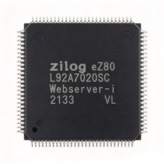
EZ80L92AZ020SG - eZ80 8-Bit MCU 20MHz ROMless LQFP-100 | Zilog
EZ80L92AZ020SG

EZ80L92AZ020SG - eZ80 8-Bit MCU 20MHz ROMless LQFP-100 | Zilog

The Zilog EZ80L92AZ020SG is an 8-bit eZ80 Acclaim! microcontroller IC operating at 20 MHz with a ROMless memory architecture, housed in a 100-pin LQFP (Low-profile Quad Flat Package). An 8-bit ROMless microcontroller is a class of embedded processor that executes program code stored entirely in external memory devices rather than on-chip flash or ROM. The ROMless approach gives system designers freedom to select external flash size, update firmware in the field, and build modular memory subsystems. The eZ80 core is a Z80-compatible architecture that executes instructions roughly 3x faster than a classic Z80 at the same clock frequency, while remaining binary-compatible with the vast Z80 software ecosystem. Key features of the EZ80L92AZ020SG include the 20 MHz eZ80 core, 24-bit linear address space supporting up to 16 MB of external memory, two UARTs with IrDA support, I2C and SPI serial interfaces, and six 16-bit timers. The device is lead-free and qualified for standard commercial temperature operation. Technically, the eZ80L92 integrates a Z80-compatible CPU core with a rich on-chip peripheral set and an external bus controller, enabling designs that mix legacy Z80 code with modern peripherals. The wide external memory interface allows glueless connection of SRAM, flash, and Ethernet companion devices from the eZ80 Acclaim! family ecosystem. Typical applications include industrial control systems, legacy Z80 equipment upgrades, Ethernet-connected embedded modules (such as the eZ80L92 module reference design), data loggers, and communication interface bridges. When designing with this ROMless device, budget external flash access wait states and lay out the address/data bus with controlled trace lengths for reliable 20 MHz operation. This page synthesizes distributor pricing, same-package drop-in alternatives, and practical design notes not found in the manufacturer datasheet alone.

USD $14.77 재고 있음
F-XC866-4FRI - 8-Bit XC800 MCU 16KB Flash 26.7MHz | Infineon
F-XC866-4FRI

F-XC866-4FRI - 8-Bit XC800 MCU 16KB Flash 26.7MHz | Infineon

The Infineon F-XC866-4FRI is an 8-bit single-chip microcontroller based on the high-performance XC800 CISC core with on-chip FLASH memory and integrated peripherals. The device operates at up to 26.7 MHz CPU clock, integrates 16 KB on-chip program FLASH and 768 B RAM, and is housed in a PG-TSSOP-38 surface-mount package. It combines a powerful 8051-compatible instruction set with embedded peripherals tuned for cost-sensitive industrial and automotive sensor applications. An 8-bit microcontroller (MCU) is a programmable logic device that integrates a CPU, non-volatile program memory, volatile data memory, and peripheral blocks onto a single silicon die. Within the broader semiconductor taxonomy, an 8-bit MCU is a sub-class of microcontroller, itself a sub-class of embedded processor, which falls under the Integrated Circuits hierarchy. The Infineon XC800 family specifically targets applications requiring deterministic real-time response, on-chip analog signal conditioning, and high immunity to automotive electromagnetic interference. Key features of the F-XC866-4FRI include a 5 V single-voltage supply with on-chip voltage regulator and on-chip oscillator, embedded ADC for analog signal acquisition, capture/compare units (CCU) for PWM generation, and a MultiCAN node for automotive network interfacing. The on-chip voltage regulator enables operation from a single 5 V supply, simplifying PCB power design, while the embedded oscillator eliminates the external crystal in many cost-driven applications. These features collectively support sensor signal acquisition, actuator control, and LIN-bus networked nodes. Architecturally, the F-XC866-4FRI employs a Harvard-style memory organization with separate program and data paths. The on-chip FLASH supports in-system programming (ISP) and in-application programming (IAP) for field firmware updates. The MultiCAN module provides hardware-accelerated CAN 2.0B frame handling, offloading the CPU and improving real-time responsiveness. The capture/compare and PWM units operate independently of the CPU, supporting high-resolution timing without software overhead. Typical applications include automotive body electronics such as door modules, seat controllers, and lighting controllers; industrial sensor signal conditioning; small motor control in HVAC dampers and pumps; and LIN-bus slave nodes communicating with a central body controller. The on-chip oscillator with PLL multiplication allows flexible clock generation without external crystals. When designing with the F-XC866-4FRI, ensure the supply decoupling follows Infineon reference design guidelines - a 100 nF ceramic capacitor close to each VDD pin plus a bulk tantalum or aluminum-polymer capacitor on the 5 V rail. The MultiCAN bus lines require external ESD protection and common-mode chokes for automotive EMC compliance, and unused GPIO pins should be configured as outputs with defined levels to minimize current leakage. This page synthesizes distributor pricing, drop-in alternatives, and practical design notes not found in the manufacturer datasheet, providing an engineer-focused overview optimized for sourcing, replacement, and design decisions.

견적 요청 문의하기
F280023PMSR - C2000 32-bit MCU, 100MHz, 64KB Flash, 64-LQFP | Texas Instruments
F280023PMSR

F280023PMSR - C2000 32-bit MCU, 100MHz, 64KB Flash, 64-LQFP | Texas Instruments

The Texas Instruments F280023PMSR is a C2000™ 32-bit real-time microcontroller from the F28002x family, featuring a C28x CPU core with FPU and TMU running at 100 MHz, paired with 64 KB (32K x 16) of flash memory and packaged in a 64-pin LQFP (PM) measuring 10x10 mm. The device integrates a single-precision floating-point unit and a trigonometric math unit, making it purpose-built for control-loop math in power-conversion and motor-drive applications. Per the LCSC distributor listing, this MPN carries the 'S' temperature grade, supporting -40°C to 125°C junction temperature in a natural convection environment. A C2000 microcontroller is a 32-bit MCU family engineered specifically for real-time control. In the broader taxonomy, the F280023PMSR sits as: microcontroller -> embedded MCU -> 32-bit MCU -> real-time control MCU -> C2000 family -> F28002x sub-family. Unlike general-purpose MCUs that prioritize connectivity or low power, C2000 devices focus on deterministic interrupt latency and high-resolution PWM generation, which are foundational for digital control of switches, motors, and power converters. Key features include the 100 MHz C28x core with hardware FPU/TMU for single-cycle trigonometric math, 64 KB flash, integrated control peripherals (ePWM, eCAP, eQEP), analog comparators and ADCs, plus InstaSPIN-FOC library compatibility. The device's FPU/TMU offloads math-intensive routines such as Park/Clarke transforms, freeing the CPU for application logic. The 64-LQFP package offers generous GPIO and a generous PCB thermal pad footprint for cost-sensitive designs. Architecturally, the F28002x combines the legacy C28x DSP-style core with a C28x+CLA-style bus matrix and a tightly-coupled control-law accelerator option in higher SKUs. The FPU executes single-precision IEEE-754 arithmetic in hardware, while the TMU accelerates sin, cos, arctan, and square-root operations used in field-oriented control (FOC) firmware. Typical applications include solar inverters, industrial motor drives (BLDC/PMSM), digital power supplies, traction inverters, and LED lighting drivers. The integrated PWM and ADC peripherals make it a strong fit for any closed-loop digital control system that demands deterministic sub-microsecond response. When designing with this part, ensure your linker script reserves the correct flash wait-state configuration for 100 MHz operation, and review the boot-ROM GPIO multiplexing table before laying out the PCB. This page synthesizes distributor pricing, same-family F28002x drop-in alternatives, and practical design notes not found in the manufacturer datasheet alone.

견적 요청 문의하기