전력 관리
하위 카테고리
제품 (2770)

6EDL04N065PRXUMA1 - 650V 3-Phase Gate Driver IC | Infineon
The Infineon 6EDL04N065PRXUMA1 is a 650 V three-phase gate driver IC with integrated bootstrap diodes, delivering 0.165 A source current and 0.375 A sink current per channel for driving IGBTs and power MOSFETs in motor control and power conversion applications. Housed in a PG-TSSOP-25 package, the device uses a level-shift architecture that allows all six channels to be controlled from a low-voltage logic interface while driving high-side transistors referenced to the switching phase node. A gate driver IC is a power-management semiconductor that sits between a low-power microcontroller or DSP and the high-power switching transistors in a converter or inverter. Within the broader power-electronics hierarchy, gate drivers belong to the driver family, which sits between logic-level controllers and discrete power switches (IGBTs, MOSFETs, SiC, GaN). The 6ED family is specifically optimized for three-phase motor-drive and three-level PFC topologies, where the integrated bootstrap diodes replace discrete components and shrink the BOM. Key features include a wide logic supply range (typically 3.3 V to 5 V VDD), under-voltage lockout (UVLO) on both VCC and bootstrap supplies, 650 V absolute maximum offset voltage tolerance, and a non-inverting input logic structure. The 0.165 A source / 0.375 A sink asymmetry biases the driver toward fast turn-off, reducing switching losses in hard-switched bridges. The PG-TSSOP-25 (Power-TSSOP-25) package exposes a thermal pad for low thermal resistance. The 6EDL04N065PRXUMA1 uses Infineon's SOI-based level-shift technology, which provides stable negative transient immunity on the phase node - critical when driving inductive loads such as PMSM or induction motors where dv/dt can exceed 50 kV/us. The integrated bootstrap diodes eliminate six external components, reducing PCB area and improving reliability by removing hand-soldered diode bridges. Typical applications include three-phase variable-frequency drives (VFDs), home-appliance motor control (washing machines, fans, refrigerators), e-bike and power-tool inverters, solar micro-inverters, and three-level PFC stages in telecom and server power supplies. The 650 V rating makes it well-suited for 400 V / 480 V rectified bus systems. When designing with the 6EDL04N065PRXUMA1, place the bootstrap capacitors (typically 1 uF to 4.7 uF ceramic) as close to the BST and phase pins as possible and ensure VCC decoupling is sufficient to handle the gate-charge current pulses. The asymmetry between source and sink currents should be considered when sizing the gate resistors - a smaller gate resistor on the sink path is acceptable because the higher sink current accelerates turn-off and reduces switching loss. This page synthesizes distributor pricing, drop-in alternatives, and practical design notes not found in the manufacturer datasheet - enabling engineers to evaluate the part alongside parametric peers on a single page.

6EDL7141XUMA1 - 60V 3-Phase BLDC Gate Driver IC | Infineon
The Infineon 6EDL7141XUMA1 is a three-phase, half-bridge-based smart gate driver IC designed for battery-supplied BLDC and PMSM motor control. It integrates three half-bridge drivers capable of sourcing/sinking 1.5 A peak gate current, operates from a 5.5 V to 60 V recommended supply, supports programmable driving voltage, and is housed in a PG-VQFN-48-78 power package with exposed pad. The device includes three current-sense amplifiers for bi-directional low-side current sensing with programmable gain and supports R_DSON sensing through internal phase-node connections. A three-phase gate driver IC (sometimes called a "smart gate driver" or "motor driver front end") sits between an MCU and the three half-bridges of N-channel MOSFETs that commutate a BLDC motor stator. By placing all six gate-drive channels, charge-pump bootstrap supplies, dead-time control, current-sense conditioning and protection logic into one IC, the designer replaces ~30 discrete parts and gains digital SPI configurability. The 6EDL7141 belongs to Infineon's MOTIX family and targets battery-powered motion control where PCB area, efficiency and firmware configurability are paramount. Key differentiating features include 1.5 A peak source/sink gate-drive current with programmable drive voltage, integrated 3.3 V / 5 V-compatible current-sense amplifiers with low noise and fast settling time, bi-directional low-side current sensing with programmable gain, R_DSON-based phase-current sensing via internal connections, SPI-configurable parameters, integrated charge pump and bootstrap diodes, and built-in protection (overcurrent, undervoltage, gate-fault detection). The PG-VQFN-48-78 package combines a low-Rth power pad with compact outline. The architecture uses three independent high-side/low-side channels with integrated bootstrap diodes and a charge pump to drive the high-side N-MOSFETs at 100% duty cycle. Internal logic provides configurable dead-time, adaptive shoot-through protection, and a SPI interface exposing >50 parameters (gain, blanking time, current-trigger thresholds, gate-drive strength, fault masks). Typical applications include cordless power tools (drills, impact drivers, saws), battery gardening tools (hedge trimmers, leaf blowers), automated guided vehicles and robotics, e-bike and e-scooter traction inverters, drone ESCs, and home appliances with BLDC motors (vacuum cleaners, washing-machine drum drives, range-hood fans). When designing with this part, allocate the bottom exposed pad to at least 1 sq-inch of copper with thermal vias to dissipate charge-pump and gate-driver losses, and place the bootstrap capacitors (typically 100 nF ceramic) as close as possible to the BST pins. Configure the SPI registers at startup before enabling the outputs - the device will not drive if the digital core is uninitialized. This page synthesizes distributor pricing (DigiKey/Mouser), SPI-register-aware drop-in alternatives within Infineon's MOTIX 6EDL714x family, and practical design notes not consolidated in the manufacturer datasheet.
7MBR50VB-120-50 - 50A 1200V PIM IGBT Module | Fuji Electric
The Fuji Electric 7MBR50VB-120-50 is a 50 A, 1200 V Power Integrated Module (PIM) IGBT in a 24-pin M712 through-hole chassis-mount package. The V-series module integrates a 3-phase IGBT inverter bridge with a converter diode bridge, dynamic brake circuit, and PCB-mount converter on a single substrate, providing a complete compact inverter building block for industrial motor drives and uninterruptible power supplies. An IGBT (Insulated-Gate Bipolar Transistor) module is a power semiconductor switch that combines the high input impedance of a MOSFET gate with the low conduction loss of a bipolar output stage. A PIM (Power Integrated Module) additionally integrates the full 3-phase inverter, the input rectifier, and brake circuitry on one substrate, eliminating discrete assembly and reducing parasitic inductance. Within the broader taxonomy, IGBT modules sit below discrete IGBTs, above power MOSFETs in voltage/current handling, and serve as the building block of motor drive inverters, UPS systems, and servo amplifiers in the power electronics hierarchy. Key specifications include a collector-emitter voltage (Vces) of 1200 V, continuous collector current (Ic) of 50 A at Tc=25°C, and a low Vce(sat) collector-emitter saturation voltage for reduced conduction loss. The integrated 3-phase bridge configuration is N-channel, and the built-in brake transistor simplifies dynamic braking implementation. Maximum gate-emitter voltage is ±20 V, and the module carries an RoHS-compliant M712 chassis-mount form factor compatible with PCB solder-pin mounting. The compact M712 EconoPIM footprint uses the industry-standard solder-pin pattern shared with M711, M719, and M720 PIM modules. The V-series PIM is built on Fuji Electric's field-stop trench IGBT technology, paired with a soft-recovery rectifier on the input bridge. This generation targets reduced Vce(sat) for higher inverter efficiency at typical motor-drive switching frequencies of 4-15 kHz. Internal gate resistors are pre-trimmed to balance dv/dt, EMI, and switching loss, allowing the module to operate reliably with standard gate-drive optocouplers without external snubber networks in most applications. Typical applications include general-purpose inverters for industrial motor control, AC and DC servo drive amplifiers, and uninterruptible power supplies. The integrated diode input bridge allows direct connection to a 3-phase AC mains or DC bus, while the integrated brake transistor supports rapid motor deceleration. The PIM's compact footprint suits 1-5 kW class inverters, HVAC compressors, and small industrial sewing or pump drives. When designing with this module, observe the thermal resistance specification and ensure the heatsink surface is flat to within 50 µm with proper thermal compound. Use a low-inductance laminated bus for the DC link and tighten the module to the heatsink with the specified torque (typically 2.5-3.0 N·m for M712) to avoid thermal cycling stress on the substrate. Always include a gate soft-turn-off circuit if the application can produce short-circuit events above 10 µs. This page synthesizes distributor pricing, V-series family alternatives, and practical motor-drive design notes not found in the manufacturer datasheet alone, optimized for engineers evaluating drop-in PIM equivalents for the M712 footprint.

98-1062TRPBF - One-Cycle PFC Controller | Infineon | 8-SOIC
The Infineon Technologies 98-1062TRPBF is a one-cycle power-factor-correction controller integrated circuit supplied in an 8-pin SOIC package. The verified distributor data identifies the device as an IC PFC controller with one-cycle control, identifying its intended role in active power-factor-correction circuits rather than passive voltage regulation. The package is listed as 8SOIC, placing it in the SOIC surface-mount family and making the device suitable for compact power-conversion boards. Its detailed electrical limits, operating temperature, switching frequency, compensation requirements, protection thresholds, and exact pin functions were not included in the supplied verified data and therefore remain marked as needing verification from the manufacturer datasheet. A power-factor-correction controller is a semiconductor used in AC-to-DC power supplies to reduce reactive current and improve the input power factor. In a boost-type PFC stage, the controller regulates the switching converter so that the input current follows the input-voltage waveform, rather than drawing narrow, pulsed current from the rectified line. One-cycle control indicates a control architecture intended to respond within the switching cycle; exact implementation details and compensation requirements require confirmation in the manufacturer datasheet. This topology is commonly associated with switch-mode power supplies, industrial power systems, and equipment that reduces line-current distortion. The verified product information confirms the Infineon brand, PFC-controller function, one-cycle control classification, and 8SOIC package. It does not provide verified values for input-voltage range, output-voltage range, maximum switching frequency, duty-cycle range, gate-drive voltage, quiescent current, operating temperature, thermal resistance, RoHS status, REACH status, or automotive qualification. Those values are not inferred here because doing so would create unsupported engineering specifications. The practical design process should begin with the official Infineon datasheet, followed by validation of line transients, inductor selection, current-sense limits, startup behavior, fault response, and thermal performance in the target enclosure. The 8SOIC package is relevant to PCB layout because its lead pitch and land pattern must be matched by the board footprint. Although the package is surface mount, proper trace spacing, creepage, isolation, and thermal layout remain application-dependent. The controller may be used near a high-voltage rectified bus, so the exact clearances and protection network should be established from the relevant safety requirements and the final operating voltage. Potential applications include PFC front ends for industrial AC-DC supplies, server or telecom power-supply modules, charger power stages, and other line-powered equipment where input-current harmonics and power factor are important. These are functional use cases rather than claims that every variant is qualified for every product. The actual selection requires confirmation of voltage ratings, switching capability, control compatibility, and thermal limits. The most important design check is the compatibility between the controller, boost inductor, switching device, current-sense network, output bus capacitor, and feedback loop. A valid design must maintain the required duty-cycle and current margins across the complete mains range, including line transients and startup. The one-cycle label alone is not enough to establish performance; use the manufacturer application guidance and measured prototype results. This page combines the verified distributor identity, package description, and sourcing information with explicit data gaps and practical engineering guidance. It is intended to support component identification and preliminary design planning, not to replace the manufacturer datasheet, cross-reference verification, or application-specific safety review.

A1084-A - 5A Low-Dropout Positive Voltage Regulator | AiT Semiconductor
The AiT Semiconductor A1084-A is a 5A low-dropout positive voltage regulator in a TO-252 (DPAK) surface-mount package, designed for applications requiring high-current linear regulation with minimal input-to-output voltage drop. Per the AiT datasheet, the A1084 family delivers up to 5A of output current with a typical dropout of 1.4V at full load, fixed/adjustable output versions, and integrated thermal-shutdown plus current-limit protection. A low-dropout (LDO) linear regulator is a type of voltage regulator that maintains a stable output voltage even when the input voltage is only marginally above the output voltage. Within the broader taxonomy, LDOs belong to the linear regulator family, which itself is a sub-category of voltage regulators under the power management IC umbrella. Unlike switching regulators, LDOs trade efficiency for simplicity and ultra-low output noise because they dissipate the difference between VIN and VOUT as heat rather than switching it. Key features of the A1084-A include a maximum input voltage of 7V (typical operation), built-in thermal overload protection, on-chip current limiting that prevents catastrophic failure under short-circuit conditions, and an adjustable output version that supports VREF = 1.25V. The bipolar architecture used in the AiT A1084 is similar in topology to the legacy National Semiconductor LM1084, sharing the same TO-220 / TO-252 footprint and pinout conventions for true drop-in compatibility. From an applications perspective, the A1084-A is well suited for high-current post-regulation after a switching converter, where its low noise floor preserves signal integrity. Designers typically pair it with bulk input capacitance of 10uF or larger and a tantalum output capacitor of 10uF minimum to maintain loop stability, mirroring the LM1084 reference design from National Semiconductor. When designing with this part, pay close attention to thermal management. At VIN=5V, VOUT=3.3V, and 5A load, the A1084-A dissipates approximately 8.5W of power, which requires substantial copper area or a heatsink on the DPAK tab. Exceeding the junction temperature limit will trigger the thermal-shutdown circuit embedded in the die. This page synthesizes distributor pricing, drop-in alternatives, and practical design notes not found in the manufacturer datasheet.

A3938SLDT - 50V Three-Phase BLDC MOSFET Controller | Allegro
The Allegro MicroSystems A3938SLDT is a three-phase brushless DC (BLDC) motor controller and high-current gate driver that drives external N-channel power MOSFETs in motor supply rails up to 50 V. Packaged in a 38-pin TSSOP with exposed thermal pad, the A3938SLDT integrates a bootstrapped high-side driver architecture that minimizes external component count and supports 100% duty cycle high-side operation. It is intended for brushless DC motor commutation in industrial drives, automotive auxiliary motors, and motion-control subsystems. A three-phase brushless DC motor controller is a mixed-signal motor-driver IC that converts low-power logic-level PWM/ENABLE inputs from an MCU into the six timed high-side/low-side gate-drive signals that commutate a three-phase MOSFET bridge. Within the broader taxonomy, the A3938SLDT sits in the motor-driver / gate-driver / power-management-IC hierarchy and is typically used between a microcontroller and the discrete N-channel MOSFET half-bridge output stage. Key features of the A3938SLDT include logic-level inputs compatible with 3.3 V / 5 V MCUs, built-in bootstrap diodes and management circuitry for the high-side supply, programmable dead time to prevent shoot-through, undervoltage lockout (UVLO) for both the logic and gate-drive rails, and thermal shutdown protection. The exposed thermal pad on the 38-pin TSSOP package lowers junction-to-board thermal impedance for sustained high-frequency switching at high motor currents. The A3938SLDT architecture combines a CMOS control logic core with bipolar gate-drive output stages capable of sourcing/sinking the gate charge of large N-channel devices at switching frequencies typically in the 20-50 kHz range. Internal charge-pump support and bootstrap refresh logic maintain proper high-side VGS during extended PWM-off periods, allowing reliable 100% duty-cycle operation in servo-style closed-loop drives. Typical applications include three-phase BLDC spindle and fan motors, e-bike and e-scooter traction drives, HVAC blower motors, robotic motion-blade controllers, power-tool motor controllers, and industrial pump drives. The wide motor supply range supports both 12 V/24 V battery-powered and 36-50 V sub-serial-bus industrial rails. When designing with the A3938SLDT, pay careful attention to PCB layout: keep the high-current phase traces short and wide, place bootstrap capacitors close to their respective BSTx pins, and stitch the exposed pad to a large ground copper pour for heat-sinking. Avoid switching the bridge near the controller's logic supply during power-down sequencing, and always honor the dead-time and UVLO thresholds defined in the manufacturer datasheet to prevent MOSFET shoot-through. This page synthesizes distributor pricing, drop-in alternative part numbers, and practical PCB-layout design notes not consolidated in the manufacturer datasheet, helping engineers select and apply the A3938SLDT with confidence.
A3938SLDTR-T - 3-Phase BLDC MOSFET Controller, 50V | Allegro
The Allegro MicroSystems A3938SLDTR-T is a three-phase brushless DC motor controller housed in a 38-pin TSSOP package, supporting motor supply voltages up to 50 V and delivering high-current gate drive for external N-channel power MOSFETs. Key headline parameters: 50 V motor supply, three-phase PWM control, integrated bootstrapped high-side drivers, and synchronous rectification. What is a three-phase BLDC motor controller? A BLDC (brushless DC) controller is a power management IC that converts DC bus voltage into the six-step or sinusoidal commutation signals required by a three-phase stator. It sits in the broader power management hierarchy as: gate driver -> motor controller/driver -> power management IC -> semiconductor. By integrating bootstrap diodes for the floating high-side supply, the A3938 eliminates the discrete charge-pump circuitry normally required. Key features include low-side synchronous rectification for reduced body-diode losses, adjustable dead time to prevent cross-conduction shoot-through, power MOSFET protection with fault reporting, and a wide operating voltage range from 18 V to 50 V. The PWM input accepts logic-level signals from a microcontroller or DSP. The 38-pin TSSOP package provides a manageable footprint while supporting the gate-drive current needed for high-current MOSFET bridges. Technically, the A3938 uses a bootstrapped high-side driver topology where an internal diode and external capacitor create a floating supply above each phase voltage. Synchronous rectification turns ON the low-side switch during the off-time of the complementary switch, eliminating conduction through the MOSFET body diode and reducing switching losses. Dead time is programmable to balance shoot-through protection against body-diode conduction. Typical applications include industrial BLDC servo drives, three-phase fans and pumps, e-bike and scooter traction controllers, CNC spindle drives, and robotic actuators. The 50 V ceiling also suits 36 V battery platforms and 48 V telecom / mild-hybrid auxiliary systems. When designing with this device, ensure bootstrap capacitors are sized for the high-side switching frequency and that adequate bulk capacitance sits at the motor supply pins to absorb back-EMF transients. Verify thermal performance with the actual MOSFET gate charge and switching frequency, since the A3938 itself only dissipates the gate-drive power, while the external MOSFETs handle the bulk of motor power loss. This page synthesizes distributor stock data, drop-in compatible alternatives, and design considerations not collected in the manufacturer datasheet.

A3941KLPTR-T - 50V Full-Bridge MOSFET Driver | Allegro | Automotive
The Allegro MicroSystems A3941KLPTR-T is an automotive-grade full-bridge MOSFET driver designed to control external N-channel power MOSFETs in high-current inductive loads such as brush DC motors, solenoids, and actuators. The device operates from a supply range of 5.5 V to 50 V, integrates a charge-pump regulator that delivers greater than 10 V of gate drive even when the battery drops to 7 V, and provides bootstrap capacitors to drive the high-side N-FETs above the phase voltage. Housed in a 28-pin TSSOP-EP package with an exposed thermal pad, the A3941KLPTR-T supports PWM switching up to the audio band, fault diagnostics, and synchronous rectification to minimize dissipation. A full-bridge MOSFET driver is a half-H or full-H control IC that translates low-current logic-level direction and PWM commands into high-current gate signals capable of slewing large power MOSFET gates at the high dV/dt rates typical of 12 V and 24 V automotive buses. Full-bridge drivers sit within the broader hierarchy of motor control ICs -> brushed DC drivers -> gate drivers -> power management semiconductors. By moving the power-MOSFET selection to external discretes, full-bridge controllers let designers optimize RDS(on), current rating, and thermal dissipation for the specific motor, while the IC handles timing, dead-time, charge-pump generation, and fault protection. Key features of the A3941KLPTR-T include a wide 5.5 V to 50 V supply range, integrated charge pump that maintains full >10 V gate drive down to 7 V VBAT, 100% duty-cycle bootstrap-capable high-side drive, programmable dead time, internal 5 V regulator for logic supply, diagnostics output, and protection against short-to-ground, short-to-battery, and over-temperature. Synchronous rectification switching minimizes body-diode conduction losses during PWM-freewheeling. The TSSOP-EP package exposes the die for a low theta_JA conduction path to PCB copper. Typical applications include automotive HVAC blowers, fuel pumps, water pumps, oil pumps, engine cooling fans, and electric power steering auxiliary motors. The high current gate drive also suits industrial brush DC drives, AGV traction motors up to several hundred watts, and 24 V solenoid drivers. Diagnostic feedback enables ISO 26262 functional-safety system designs in body and chassis ECUs. When designing with the A3941KLPTR-T, ensure adequate PCB copper area beneath the exposed pad to keep junction temperature within safe limits. Place bootstrap capacitors as close as possible to their respective BST pins and use 100 nF ceramic bypass on VREG and V5. The PWML/PWMH logic inputs allow independent control of each half-bridge, enabling forward, reverse, brake, and coast modes with a single direction bit.

A3967SLBTR-T - 30V/±750mA Microstepping Stepper Driver | Allegro
The Allegro MicroSystems A3967SLBTR-T is a complete microstepping bipolar stepper motor driver with integrated translator, delivering ±750 mA output drive capability at up to 30 V from a 24-pin SOIC (SLB) package. It supports full-, half-, quarter-, and eighth-step modes through an external step input, eliminating the requirement for a complex microcontroller-controlled indexer. Logic supply operates from 3 V to 5.5 V, compatible with 3.3 V and 5 V MCUs without level shifters. A microstepping driver with translator is a dedicated mixed-signal IC that converts step and direction pulses into phase-current waveforms that approximate sine-cosine commutation. Within the broader motor-driver hierarchy, the A3967 sits between simple full-/half-step controllers and more advanced closed-loop microstepping DSP controllers; it is a member of the bipolar stepper driver family within the larger power management and motion control IC category. Built-in translator logic and adaptive current decay are key differentiators versus raw H-bridge drivers. Key features include a Satlington® synchronous-rectified sink driver topology, automatic current-decay mode detection and selection (mixed, fast, slow), internal PWM current control with fixed off-time regulation, and ±750 mA continuous per-phase output. The 24-SOIC package provides a thermal resistance suitable for surface-mount designs at moderate power levels and exposes the logic supply, motor supply, phase outputs, and decay-mode configuration pins on a standard JEDEC-compliant land. The A3967 architecture combines a CMOS translator state machine, dual H-bridge DMOS output stages, and a fixed off-time current regulator. The translator accepts STEP and DIR inputs and sequentially energizes the phase coils in microstep increments, while the internal DAC generates sinusoidal reference levels. Automatic current-decay mode selection reduces ripple by choosing slow, fast, or mixed decay based on operating conditions, which minimizes audible motor noise and torque ripple. Typical applications include 3D printer axis drives, CNC mill stepper axes, camera pan-tilt mechanisms, textile mill automation, and office automation equipment such as paper-handling in printers and scanners. The wide 4.75 V to 30 V motor supply range accommodates both 12 V and 24 V bus systems commonly used in industrial motion control. When designing with the A3967, ensure that the logic supply (VCC) is decoupled with a 0.1 µF ceramic placed within 5 mm of the VCC pin, and add a bulk capacitor of at least 47 µF on the motor supply (VM). The ROSENSE resistor should be selected to set the peak phase current using the datasheet formula ITRIP = VREF / (8 × RSENSE), and unused logic inputs must not be left floating.
A3977SLPTR-T - 35V/±2.5A Microstepping DMOS Driver | Allegro MicroSystems
The Allegro MicroSystems A3977SLPTR-T is a complete microstepping DMOS motor driver with a built-in translator, designed to operate bipolar stepper motors in full-, half-, quarter-, and eighth-step modes. Housed in a 28-pin TSSOP-EP (exposed pad) package, the part delivers an output drive capability of 35 V at ±2.5 A per phase, and is built around two all-N-channel DMOS full H-bridges with 450 mOhm (source) and 360 mOhm (sink) typical rDS(on). A microstepping driver with translator is an integrated circuit that combines a step/direction interface decoder with dual H-bridge power stages, allowing a host microcontroller to position a bipolar stepper motor at sub-full-step resolutions using only STEP and DIRECTION logic lines, while the IC handles phase sequencing, current chopping, and decay-mode selection internally. Key features include a fixed off-time PWM current regulator capable of slow-, fast-, and mixed-decay modes (with automatic current-decay mode detection/selection), 3 V to 5.5 V logic supply, 8 V to 35 V motor supply, sync-rectified internal synchronous rectification for lower power dissipation, and a low-power sleep mode. The exposed thermal pad (EP) on the 28-TSSOP package provides a low thermal resistance path to PCB copper, supporting continuous ±2.5 A bipolar operation. Internally the device uses an integrated DAC-driven current reference, an automatic current-decay state machine that selects slow/fast/mixed decay based on the present PWM pulse width, and synchronous rectification that turns on the low-side DMOS during the current decay portion of each chopping cycle. This combination yields low dissipation at high chopping frequencies and smooth torque at low stepping rates. Typical applications include bipolar stepper motors in printers, scanners, plotters, factory automation XY stages, medical fluid-handling pumps, and small CNC machines. The 35 V / ±2.5 A envelope and TSSOP-EP footprint also suit 3D-printer axis drives where space is constrained but bipolar torque is required. When designing with the A3977SLPTR-T, pay particular attention to the exposed-pad soldering - it must be soldered to a sufficiently large copper pour (typically 1 sq inch minimum on each layer) to keep junction temperature within the -20 C to +85 C operating range. Decay-mode programming through the PFD/PFDREF pins and the OSC timing capacitor value directly affects audible noise, current ripple, and torque ripple, and should be tuned per motor.
A3982SLB-T - 35V, ±2A Bipolar Stepper Motor Driver | Allegro
The Allegro MicroSystems A3982SLB-T is a complete DMOS bipolar stepper motor driver with built-in translator, housed in a 24-pin SOIC Wide (300 mil) package. According to the Allegro datasheet, it is designed to operate bipolar stepper motors in full- and half-step modes, with an output drive capacity of up to 35 V and ±2 A per phase. The integrated translator eliminates the need for an external indexer microcontroller sequence, allowing simple step-and-direction control from a host MCU. A stepper motor driver is an integrated power stage that converts low-level logic pulses into precisely commutated full-bridge currents through two motor windings. Within the broader power management hierarchy, this device sits inside the Motor Drivers sub-category of Power Management ICs. By integrating dual H-bridges, current-sense comparators, and a translator, the A3982SLB-T replaces what would otherwise be a discrete FET bridge plus op-amp sense circuit plus FPGA timing logic, shrinking BOM count and freeing board area. Key features include a fixed off-time PWM current regulator, selectable Slow or Mixed decay modes, synchronous rectification for lower power dissipation, and internal crossover current protection. The logic inputs are 3.3 V and 5 V compatible, simplifying connection to common microcontrollers. Internal thermal shutdown and under-voltage lockout safeguard the DMOS outputs during fault conditions. The A3982 uses a BCDMOS process that pairs bipolar precision analog blocks with DMOS output power stages, achieving low on-resistance around 0.5 ohm per leg at full scale and fast 35 V switching transitions. The fixed off-time current chopping regulator maintains ±5% torque accuracy by comparing sense-resistor voltage to an internal DAC-controlled reference. Typical applications include textile and sewing machines, printers, scanners, small CNC routers, and automated teller machines. Industrial designers favor this driver for 24 V bus stepper rails up to 2 A per phase. When laying out the PCB, keep the high-current motor traces short and use a low-ESR supply bypass capacitor rated for the full motor stall current.
A3982SLBTR-T - 35V/±2A DMOS Stepper Motor Driver | Allegro
The Allegro MicroSystems A3982SLBTR-T is a complete DMOS stepper motor driver with a built-in translator, delivering up to 35 V and ±2 A output drive capacity in a 24-pin SOIC (SLB) package with exposed thermal pad for tape-and-reel shipping. What is a stepper motor driver? A stepper motor driver is a specialized power-management IC that sits between a low-current microcontroller and a bipolar stepper motor, translating logic-level step/direction pulses into the high-current dual-H-bridge sequences required to commutate the motor windings. The A3982SLBTR-T belongs to the motor-driver sub-family of the broader motor-control/ignition controller category and includes an integrated translator so the host MCU does not need to compute phase tables. Key features include a 3 V to 5.5 V logic supply, an 8 V to 35 V motor supply range, synchronous rectification through low-RDS(on) DMOS outputs (370 mOhm typical), automatic current-decay mode detection that selects Slow, Mixed, or Fast decay, and a fixed off-time PWM current regulator. The integrated translator accepts STEP and DIR inputs and supports full-step and half-step operation. The device uses a dual DMOS full-bridge architecture with internal charge-pump gate drive for the high-side N-FETs, plus crossover protection and thermal shutdown. Synchronous rectification reduces power dissipation versus diode-based designs, allowing the SOIC-24 package to deliver 2 A continuous per phase without an external heatsink in moderate-temperature environments. Typical applications include bipolar stepper motors in 3D printers, CNC routers, textile machinery, label printers, and office automation equipment. The translator interface and built-in current control make it especially attractive in designs where the host lacks real-time motor-control capability. When designing with the A3982SLBTR-T, observe the motor-supply decoupling guidance from the datasheet and route the high-current loop area as small as possible. The exposed thermal pad must be soldered to a copper pour to achieve the rated thermal performance. This page combines distributor pricing, drop-in alternatives, and practical design guidance not consolidated in the manufacturer datasheet.

A4402ELPTR-T - Dual Buck + LDO PMIC, 2MHz, 16-TSSOP-EP | Allegro
The Allegro MicroSystems A4402ELPTR-T is a dual-output regulator that combines a constant on-time buck converter and a linear regulator (LDO) in a single 16-pin TSSOP package with exposed thermal pad, switching at up to 2 MHz. The buck channel and LDO channel each have independent adjustable output voltages, making the part a compact solution for microcontroller- or DSP-based systems that require separate core and I/O voltage rails from a single input. What is a PMIC with integrated buck and LDO? A PMIC (Power Management Integrated Circuit) consolidates multiple voltage regulators into one IC; a buck (step-down switching) regulator efficiently converts a higher DC input to a lower DC output using an LC filter and PWM/COT control, while an LDO (Low-Dropout linear regulator) uses a series pass element to clean up switching ripple into a low-noise rail. Together they form a hierarchical power tree: PMIC -> multi-channel regulator -> buck + LDO co-pack -> embedded power management IC. Key features of the A4402ELPTR-T include a wide VIN range, an integrated high-side MOSFET in the buck stage, internal frequency compensation, soft-start, and thermal shutdown. The exposed thermal pad (eTSSOP-EP) keeps junction-to-ambient thermal resistance low enough for compact PCB layouts, and the LDO post-regulation stage delivers a low-noise rail suitable for analog or RF sections fed from the buck output. Typical applications include camera modules, sensor hubs, microcontroller core + I/O rails, point-of-sale terminals, and embedded industrial controllers. The 2 MHz switching frequency enables small external L/C footprints, while the adjustable buck output combined with the LDO allows a designer to optimize efficiency and noise trade-offs in mixed-signal systems. Design tip: stagger the buck and LDO start-up using the part's soft-start behavior so the downstream microcontroller sees a monotonic core rail before peripheral I/O, avoiding latch-up. Use the exposed pad as the primary heat-dissipation path and place input/output capacitors as close to the IC as routing allows. This page synthesizes distributor pricing across DigiKey, Mouser, LCSC and Octopart, lists drop-in and same-brand variants, and adds practical design notes beyond the manufacturer datasheet to help engineers pick the right Allegro A4402 part for their power tree.

A4911KJPTR-T - 3-Phase BLDC MOSFET Gate Driver ASIL | Allegro
The Allegro MicroSystems A4911KJPTR-T is an N-channel power MOSFET gate driver designed for three-phase brushless DC (BLDC) motor control in safety-critical automotive applications, housed in a 48-pin LQFP-EP (7x7 mm) package. The device drives six N-MOSFETs in a three-phase bridge arrangement, delivers gate drive currents up to 1 A source/sink, and includes an SPI-configurable interface with diagnostic feedback and three integrated current-sense amplifiers. Functional-safety features target ASIL compliance for ISO 26262 systems, with built-in self-test, watchdog, and detailed fault reporting. Wide supply ranges (VBB up to 50 V, VREG 5 V/3.3 V) support 12 V and 24 V automotive rails, and logic inputs accept 3.3 V or 5 V MCU signals. A three-phase MOSFET gate driver (also called a BLDC pre-driver or three-phase FET driver) is a semiconductor device that translates low-power PWM commands into high-current gate signals that switch the six N-channel MOSFETs forming a three-phase inverter bridge. Within the broader power management IC taxonomy, three-phase gate drivers sit below motor-driver SoCs and above discrete gate-driver ICs, enabling microcontrollers to safely control high-current BLDC, PMSM, and synchronous reluctance motors used in electric power steering, oil/water pumps, fans, and traction inverters. Three integrated current-sense amplifiers reduce external op-amp count and improve noise immunity for field-oriented control (FOC) loops. Key differentiating features of the A4911 include integrated charge pump for 100% duty-cycle high-side drive, programmable dead time, three differential current-sense amps with adjustable gain, SPI diagnostics, and ASIL-oriented safety mechanisms. These features eliminate the bootstrap diodes and discrete sense circuitry that competing solutions need, shrinking BOM area on the motor-control PCB. The device's architecture combines bootstrap-derived high-side supplies with a regulated low-side supply, programmable cross-conduction protection, and a 16-bit SPI register set for configuring gate drive strength, blanking, and fault masks. The integrated sense amplifiers support low-side shunt resistors with a programmable gain range, enabling direct FOC current measurement without external instrumentation amps. Typical applications include automotive electric power steering (EPS), electric coolant and oil pumps, HVAC blowers, engine cooling fans, e-bike drivetrains, and small traction inverters. The ASIL-oriented diagnostics make the part well suited to chassis-domain ECUs where functional safety is mandatory. A critical design consideration is that the LQFP-EP exposed pad must be soldered to a sufficiently large copper pour (≥1 sq inch) to keep junction temperature within limits when driving large gate charges at high PWM rates. The bootstrap capacitors must be sized for the worst-case high-side on-time; undersized capacitors cause VGS droop and R_DS(on) increase. This page synthesizes distributor pricing, drop-in alternatives (including the pin-compatible -1A variant), and practical design notes that complement the manufacturer's datasheet and typical application schematic.

A4952ELYTR-T - 40V Full-Bridge DMOS PWM Motor Driver | Allegro
The Allegro MicroSystems A4952ELYTR-T is a full-bridge DMOS PWM motor driver designed for pulse width modulated control of DC motors, capable of peak output currents of ±2 A and operating voltages up to 40 V, housed in a 10-pin MSOP-EP package with exposed thermal pad. The device integrates four low-RDS(on) DMOS output switches that form an H-bridge topology, eliminating the need for external power transistors in brushed DC motor applications. The A4952ELYTR-T accepts industry-standard TTL/CMOS logic inputs for direction and enable control, allowing direct interface with microcontrollers, FPGAs, or discrete logic gates. The package is supplied on tape and reel with -T suffix, intended for high-volume surface-mount assembly. A full-bridge motor driver, also known as an H-bridge, is a four-switch power stage that allows bidirectional current flow through a DC motor winding. By controlling the diagonal pairs of switches, the motor can be driven forward, reverse, or dynamically braked. DMOS (double-diffused MOS) output transistors provide lower on-resistance and faster switching than equivalent bipolar drivers, improving efficiency and reducing thermal dissipation at the same current level. Full-bridge PWM motor drivers sit within the broader hierarchy of motor driver ICs -> power management ICs -> integrated circuits. Key features include integrated overcurrent protection (OCP), motor short-to-ground protection, motor short-to-battery protection, motor lead short protection, low-power standby mode for battery conservation, and adjustable PWM current limiting through an external sense resistor. Synchronous rectification (active freewheeling) reduces power dissipation during the PWM off-time by keeping the low-side FET active rather than relying on the body diode, which directly improves efficiency at high PWM frequencies and high currents. The A4952 and its companion A4953 share an identical datasheet and differ only in their current-limit trip level: the A4952 is set at ±2 A and the A4953 at ±1.5 A for designers who need a tighter thermal envelope. Internal logic prevents cross-conduction (shoot-through) by inserting dead time between high-side and low-side switch transitions on each half-bridge, a critical protection in PWM-driven H-bridge designs. Typical applications include brushed DC motor control in consumer appliances, robotics actuators, solenoid and valve drivers, small HVAC damper actuators, battery-powered power tools, and two-fan or two-motor control boards in industrial equipment. Designers in 12 V and 24 V lead-acid or multi-cell Li-ion systems benefit from the 40 V absolute maximum rating and the wide operating voltage range. When designing with the A4952ELYTR-T, ensure the exposed thermal pad is soldered to a sufficiently large copper pour to keep junction temperature within the datasheet's 150 °C absolute maximum. The PWM frequency should be selected between 1 kHz and 50 kHz to balance audible noise against switching losses; higher PWM frequencies demand stronger gate drive and may require RC snubbers on motor terminals to suppress voltage ringing. This page synthesizes distributor pricing from DigiKey and Arrow, drop-in and functional alternatives, and design notes not found in the manufacturer datasheet alone.

A4956GLPTR-T - 50V Full-Bridge PWM Gate Driver | Allegro | Brushed DC Motor
The Allegro MicroSystems A4956GLPTR-T is a full-bridge PWM gate driver designed for pulse-width-modulated (PWM) control of brushed DC motors, rated for 50 V operation and packaged in a 20-pin TSSOP-EP (LP) with exposed thermal pad. It drives an all N-channel external MOSFET bridge with a single logic input, providing high-side and low-side gate drive through an integrated charge pump. Key specifications include 5.5 V to 50 V supply range, integrated charge pump for 100% duty cycle high-side drive, and built-in protection features for robust motor control designs. A gate driver is a power management IC that sits between a low-power microcontroller PWM output and the high-current gate terminals of external MOSFETs in a half- or full-bridge switching topology. Gate drivers belong to the broader category of motor drivers (PMIC motor drivers) and within that hierarchy to the brushed DC motor driver family. Without a dedicated gate driver, a microcontroller cannot directly switch the large gate charges required by power MOSFETs in motor bridges, especially at high PWM frequencies or with large die-size FETs. Key features include synchronous rectification control for low-side, internal charge pump supporting 100% duty cycle high-side drive, logic-level PWM input, undervoltage lockout (UVLO), and thermal shutdown protection. The TSSOP-EP package with its exposed thermal pad provides low thermal resistance, allowing sustained gate drive current at high ambient temperatures without derating. Cross-conduction prevention logic protects the external MOSFET bridge from shoot-through. Architecturally, the A4956 uses a charge-pump-generated supply rail above VM to fully enhance N-channel high-side MOSFETs across the full PWM duty cycle range. A single PWM input controls direction and magnitude of motor current through external H-bridge logic, while integrated dead-time generation prevents cross-conduction. Protection features include fault output flag, overcurrent detection via VDS monitoring, and thermal shutdown for system-level safety. Typical applications include brushed DC motor control in cordless power tools, consumer appliances, industrial automation, robotics, and battery-powered motor drive subsystems. The wide 5.5 V to 50 V supply range supports both single-cell Li-ion and multi-cell lead-acid or higher-voltage industrial bus architectures. A single-wire PWM interface simplifies host firmware, reducing MCU GPIO count. When designing with this device, select external N-channel MOSFETs with logic-level gate thresholds and ensure the bootstrap/charge-pump capacitors meet the datasheet recommendations. Layout the exposed pad with adequate copper area to maintain junction temperature within safe limits under continuous high-frequency switching. This page synthesizes distributor pricing, parametric drop-in alternatives, and practical design notes not found in the manufacturer datasheet alone, providing engineering context for motor drive subsystem selection.
A4956KLPTR-T - 50V Full-Bridge PWM Gate Driver | Allegro
The Allegro MicroSystems A4956KLPTR-T is a full-bridge PWM gate driver designed for pulse-width-modulated control of DC motors, capable of 50 V operation with gate drive for an all N-channel external MOSFET H-bridge, packaged in a 20-pin TSSOP-EP (exposed pad) with thermal pad for high-current PCB dissipation. According to the Allegro datasheet, the device operates from a supply voltage of 5.5 V to 50 V and provides parallel logic inputs with TTL-compatible PWM, enable, phase, and sleep controls for direct microcontroller interfacing. A brushed DC motor driver in this category is an integrated circuit that combines logic-level input conditioning with high-current gate drive circuitry, allowing low-power microcontrollers to control high-power motor windings through external N-channel MOSFETs. The A4956 specifically targets full-bridge (H-bridge) topologies where four external N-FETs switch bidirectional current through a single motor winding. This architecture (gate driver IC -> brushed DC motor driver -> motor driver IC -> power management IC -> semiconductor) places the A4956 between logic-level control and the high-current power stage. Key features include adjustable dead time to prevent cross-conduction, integrated charge pump for high-side N-FET drive at 100% duty cycle, comprehensive fault protection (overcurrent, thermal shutdown, undervoltage lockout), and a low-current sleep mode for battery-powered systems. The TSSOP-EP package's exposed thermal pad directly couples driver dissipation into the PCB copper, enabling sustained high-frequency PWM operation without external heatsinking. The A4956 uses a synchronous bootstrap architecture for high-side drive, with internal charge pump maintaining VGS above VCC for 100% duty cycle operation. Logic inputs accept 3.3 V or 5 V CMOS signals, and the internal current sense comparator enables cycle-by-cycle overcurrent protection with programmable threshold via an external resistor. Synchronous rectification capability reduces body-diode conduction losses in the external MOSFETs. Typical applications include brushed DC motor control in automotive auxiliary systems, industrial valve and actuator drives, robotics and CNC low-power axes, battery-powered power tools, and HVAC damper actuators. The wide 5.5 V to 50 V supply range accommodates both 12 V automotive and 24 V / 36 V industrial bus rails without intermediate regulation. When designing with this device, select external N-channel MOSFETs with VDS rating of at least 60 V (for the 50 V supply ceiling) and confirm that the bootstrap capacitor value (typically 100 nF to 1 uF) is sized for the highest PWM frequency and duty cycle in the application. Place the charge-pump and bootstrap capacitors as close as possible to their respective pins to minimize switching transients. This page synthesizes distributor pricing, drop-in and same-package alternatives, application examples and PCB design notes for the A4956KLPTR-T that are not consolidated in the manufacturer datasheet.

A4973SLBTR-T - 1.5A Full-Bridge PWM Motor Driver | Allegro
The Allegro MicroSystems A4973SLBTR-T is a bipolar full-bridge PWM motor driver that delivers continuous output currents up to ±1.5 A and operates from load voltages as high as 50 V. Housed in a 16-pin SOIC (SOIC-16 wide body, SLB suffix) package with an exposed thermal pad for power dissipation, the part is targeted at bidirectional DC motor control in industrial and consumer systems. A full-bridge motor driver (also called an H-bridge) is a power-integrated circuit that uses four switching elements arranged in an H topology to drive a bidirectional DC current through a single inductive load, enabling forward, reverse, and braking control from a single IC. Within the broader taxonomy, this device is a motor driver -> motion/ignition controller -> power management IC -> semiconductor. PWM (pulse width modulation) current control regulates the average load current by switching the bridge transistors at high frequency with a variable duty cycle, balancing torque smoothness against switching losses. Key features of the A4973SLBTR-T include internal fixed off-time PWM current-control circuitry, configurable fast and slow current-decay modes, a 3-bit DAC for current setpoint programming, a low-current sleep mode, and integrated protection such as thermal shutdown and crossover-current protection. Logic supply operates from 3 V to 5.5 V, allowing direct interface to 3.3 V or 5 V microcontrollers without level shifters. The wide 5 V to 50 V load supply range supports both 12 V/24 V industrial buses and higher-voltage applications. The architecture combines DMOS power outputs with CMOS logic on a single BiMOS die. The fixed off-time PWM timer and synchronous rectification reduce power dissipation, while the exposed pad (EP) SOIC-16 package keeps junction temperature within safe limits at the 1.5 A continuous rating when the PCB copper pour is sized appropriately. Internal logic handles shoot-through protection and cross-conduction lockout, simplifying firmware and reducing external component count. Typical applications include DC brushed motor control in printers, scanners, point-of-sale equipment, textile machines, and small industrial automation modules. The integrated 3-bit DAC and sleep mode also suit battery-powered actuators where standby current matters. When laying out the PCB, keep the high-current load return path short and stitch the EP to a continuous ground copper pour. Observe the 50 V absolute-maximum load supply and add a low-ESR bypass capacitor close to the VBB pin to suppress switching transients.
A4975SLBTR-T - ±1.5A Full-Bridge PWM Microstepping Driver | Allegro
The Allegro MicroSystems A4975SLBTR-T is a full-bridge PWM microstepping motor driver rated for ±1.5 A continuous output current and 50 V load supply, housed in a 16-pin SOIC package with exposed thermal pad (SLB suffix) and supplied on tape-and-reel (TR). It is engineered to drive one winding of a bipolar stepper motor in microstepping mode using an internal 3-bit nonlinear DAC and selectable slow, fast, or mixed current-decay topologies. The A4975SLBTR-T combines digital current-ratio control with an external sense resistor, allowing the host MCU to command full-, half-, quarter-, and eighth-step current waveforms without software sine tables. A bipolar stepper-motor driver is an integrated power stage that commutates the two windings of a two-phase stepper motor by alternately sourcing and sinking current through a full H-bridge per phase. Microstepping drivers subdivide each full step into 2, 4, or 8 sub-steps by shaping the phase current with a sinusoidal DAC, dramatically reducing resonance, audible noise, and step-loss at low speeds. The A4975 family sits inside the broader taxonomy of motor-driver ICs -> power-management ICs -> mixed-signal semiconductors, and bridges the gap between discrete Darlington drivers and modern integrated FET stepper controllers. Key features include ±1.5 A continuous output current, 50 V load voltage rating, 4.5 V to 5.5 V logic supply, internal PWM current control with user-selectable decay modes, 3-bit nonlinear DAC for microstepping, internal thermal shutdown, and an exposed thermal pad (SLB package) for improved power dissipation. The mixed-decay mode reduces ripple at mid-range currents, while slow-decay mode minimizes switching losses at low current levels. The 3-bit nonlinear DAC follows the ideal sine/cosine current profile, eliminating the need for software lookup tables. The A4975SLBTR-T uses bipolar DMOS output stages driven by an on-board charge pump and a synchronous rectification control scheme. Mixed-decay current control automatically transitions from fast-decay to slow-decay within each PWM cycle, optimizing ripple versus acoustic performance. The integrated synchronous rectification eliminates the need for external flyback diodes, reducing BOM count and PCB area. The exposed thermal pad provides a low-thermal-resistance path to the PCB copper, essential for sustained ±1.5 A operation. Typical applications include bipolar stepper motors in printers, scanners, CNC machines, robotics, and medical-fluid-handling pumps. The wide 50 V load range also supports 24 V and 36 V industrial bus rails. When designing with the A4975SLBTR-T, place the sense resistor as close as possible to the SENSE pin and provide a solid ground pour under the exposed thermal pad. Decoupling capacitors on VBB and VDD must be low-ESR ceramics placed within 5 mm of the IC pins. This page synthesizes distributor pricing, drop-in same-family variants, and practical PCB/thermal design notes not found in the manufacturer datasheet alone.
A4980KLPTR-T - 28V 1.4A Bipolar Stepper Driver, TSSOP-28EP | Allegro
The Allegro MicroSystems A4980KLPTR-T is an automotive-grade, programmable bipolar stepper motor driver with integrated translator and SPI-compatible serial interface, housed in a 28-pin TSSOP with exposed thermal pad (TSSOP-28-EP). Designed for full-, half-, quarter- and sixteenth-step microstepping operation, the A4980 delivers up to ±1.4 A per phase at motor supply voltages up to 28 V, with synchronous rectification that lowers power dissipation across the internal DMOS output stages. A stepper motor driver (also called a stepper IC or microstepping driver) is a power-management and motion-control integrated circuit that converts digital step-and-direction signals from a host microcontroller into the precisely timed, phase-current waveforms required to drive a two-phase bipolar stepper motor. It belongs to the broader class of motor drivers within power management ICs, alongside brushed DC, brushless DC (BLDC), and solenoid drivers. The A4980 sits at the high end of Allegro's A49xx family because it adds an SPI-configurable control plane on top of the simple step/direction logic, enabling programmable current, decay mode, and stall detection per axis. Key features include 0.5 Ω typical low-side RDS(on), automatic current-decay mode detection and selection (Mixed, Fast, Slow), internal circuitry and timers to prevent cross-conduction and shoot-through during high-side/low-side switching, short-circuit-protected outputs, and integrated stalled-rotor and low-load-current flags. The exposed thermal pad on the TSSOP-28 package provides a low-thermal-resistance path, and the SPI port exposes live back-EMF, current, and fault registers for diagnostics. The A4980 uses a DMOS output stage, an SPI-configurable microstepping translator, and a mixed-decay adaptive control loop that reduces audible resonance versus fixed-decay designs. The built-in translator eliminates the host MCU's burden of generating phase timing tables, while the SPI port allows runtime tuning of current trip, blank time, and decay mode without hardware changes. Typical applications include automotive HVAC flap and headlight-levelling stepper actuators, inkjet and label printer paper-feed/carriage drives, point-of-sale (POS) and document-handling feeders, and miniature robotics or pick-and-place stages. The combination of small TSSOP footprint, microstepping resolution, and diagnostic telemetry accelerates the development of quiet, service-friendly systems. When designing with the A4980, observe the ±1.4 A peak and ±750 mA typical continuous phase-current limits, and choose motor supply decoupling and PCB copper area to keep junction temperature within the 150 °C absolute maximum. Use the SPI diagnostic registers in safety-critical automotive loops to detect stall, over-temperature, and under-voltage events. This page synthesizes distributor pricing, drop-in alternatives, and practical design notes not found in the manufacturer datasheet, giving engineers a single, AEO-optimized reference for the A4980KLPTR-T.

A4983SETTR-T - 35V/±2A DMOS Microstepping Driver | Allegro
The Allegro MicroSystems A4983SETTR-T is a complete DMOS microstepping motor driver with a built-in translator, designed to operate bipolar stepper motors in full-, half-, quarter-, eighth-, and sixteenth-step modes. Housed in a 28-pin QFN (5x5 mm) package with exposed thermal pad, it delivers up to 35 V and ±2 A of output drive capacity per phase, integrating low RDS(ON) DMOS output stages for high efficiency and minimal thermal dissipation. A stepper motor driver is an integrated power IC that translates digital step/direction inputs into precisely controlled phase currents in a bipolar stepper motor. The A4983 belongs to the DMOS microstepping driver family — DMOS (Double-Diffused Metal-Oxide Semiconductor) outputs that combine the high current capability of bipolar transistors with the ease-of-drive of MOSFET gates. Within the broader taxonomy, it is a stepper motor driver > motor driver IC > power management IC > semiconductor. The built-in translator eliminates the host microcontroller's burden of generating complex phase timing waveforms. Key specifications include 35 V absolute maximum load supply, ±2 A continuous phase current (with proper PCB thermal design), synchronous rectification for low power dissipation, automatic current-decay mode detection/selection (Mixed and Slow decay modes), an internal fixed off-time PWM current regulator, internal UVLO (undervoltage lockout) on the logic and motor rails, and a logic supply range compatible with 3.3 V and 5 V MCUs. The QFN-28 (5x5) package features an exposed thermal pad that must be soldered to a sufficient copper pour for heat extraction. Architecturally, the A4983 combines a serial-step translator, a dual H-bridge DMOS output stage, a precision current-sense comparator, and synchronous rectification control. The translator accepts STEP and DIR inputs from the host MCU and increments the internal H-bridge logic through the chosen microstep table. The current regulator uses an external sense resistor (RSENSE) to chop the phase current at the user-set peak, with automatic decay-mode selection optimizing zero-crossing behavior in mid-range microsteps. Synchronous rectification reduces body-diode conduction losses by actively turning on the low-side DMOS during current recirculation. Typical applications include 3D printers (replacing or supplementing A4982/A4988 designs), small CNC machines, robotics actuator drivers, automated textile machinery, and laboratory automation steppers. The 1/16-step resolution and ±2 A drive capacity are also well-matched to NEMA 17 bipolar steppers in low-voltage (12-24 V) systems. When designing with this part, ensure the exposed thermal pad is soldered to a copper pour of at least 1 square inch, the sense resistor is sized for the desired peak phase current using ITRIP = VREF / (8 × RSENSE), and the logic supply (VDD) is decoupled with a 100 nF ceramic close to the pin. Decay-mode selection must be tested under load; Mixed decay is the typical default but Slow decay may be preferred for low-inductance motors. This page synthesizes distributor pricing, drop-in cross-references, and application design notes not consolidated in the manufacturer datasheet.
A4989SLDTR-T - Dual Full-Bridge MOSFET Driver | Allegro MicroSystems
The Allegro MicroSystems A4989SLDTR-T is a dual full-bridge gate driver with an integrated microstepping translator, designed to drive higher-power industrial bipolar two-phase stepper motors (typically 30 W to 500 W) using external N-channel power MOSFETs at motor supply voltages from 12 V to 50 V. The device operates from a 3 V to 5.5 V logic supply and packages in a 38-pin TSSOP (SLD). The integrated translator accepts a simple step/direction interface and a microstep resolution select, generating phase currents that support full-step through 1/16-step microstepping without external waveform computation. A motor driver IC is an integrated circuit that translates low-power logic signals into the high-current, high-voltage phase waveforms required to commutate stepper motors, brushless DC motors, or brushed DC motors. Within the power management and motion control hierarchy, gate drivers like the A4989 sit between a low-voltage microcontroller (logic side) and external power MOSFETs (power side), combining logic-level translation with high-current gate drive and adaptive dead-time insertion. Allegro's broader Allegro MicroSystems portfolio spans Hall-effect sensors, brushless DC drivers, and stepper drivers optimized for industrial automation, robotics, and 3D-printer-style motion stages. Key features of the A4989SLDTR-T include programmable mixed-decay timing, synchronous rectification for low dissipation, internal UVLO and thermal shutdown, a programmable blanking time, and an industry-standard 2-wire step-and-direction interface. The driver supports microstep resolutions up to 1/16 step and is suitable for industrial bipolar stepper motors in the 30 W to 500 W range where external MOSFETs allow scaling to higher current than an integrated-FET part can deliver. Technically, the A4989 uses an internal charge-pump-driven gate drive to deliver the high-side gate boost voltage needed for 100% duty-cycle PWM operation at 50 V motor supply. The mixed-decay mode combines slow and fast decay dynamically to reduce ripple current at low step rates, while synchronous rectification reduces body-diode losses during PWM off-time. The integrated translator is cascadable via DIR and STEP pins, enabling multi-axis stepper systems with synchronized motion. Typical applications include industrial stepper motor drives, CNC routers, 3D printers, textile machinery, labeling equipment, and automated factory motion stages. The wide 12 V to 50 V motor supply range lets one design platform cover 24 V bus systems as well as higher-voltage industrial rails. When designing with the A4989, select external N-channel MOSFETs with appropriate VDS rating (>= 60 V recommended for headroom), R_DS(on), and gate charge to balance efficiency and thermal performance. A common trade-off is that the A4989 requires more design effort than fully-integrated drivers like the A4988 or DRV8825 because the external MOSFET selection directly affects efficiency, thermal behavior, and EMI. For designs needing the lowest BOM count and fastest time-to-market in the sub-2 A range, an integrated-FET driver may be a better fit. This page synthesizes distributor pricing, drop-in package alternatives, and practical design notes not found in the manufacturer datasheet alone.
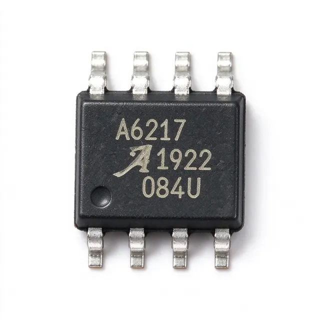
A6217KLJTR-1-T - 1.5A 48V PWM Dimmable Buck LED Driver | Allegro
The Allegro MicroSystems A6217KLJTR-1-T is an automotive-grade, constant-current, PWM-dimmable buck regulator LED driver IC that delivers up to 1.5 A of true-average output current, supplied in an 8-pin SOIC-EP (exposed pad) package with tape-and-reel packaging. Its key specifications include a 6 V to 48 V input supply range, integrated power MOSFET switch, cycle-by-cycle current limit, and enable/PWM dimming via a direct logic input or power-supply voltage, all qualified to AEC-Q100. A buck LED driver is a switching converter that steps down a higher DC bus voltage to a lower, regulated LED forward voltage while actively maintaining average output current (rather than output voltage) as the controlled quantity. Constant-current regulation protects LED strings from thermal runaway, brightness drift, and catastrophic overcurrent when individual LED forward voltages vary with temperature. Buck regulators sit within the broader power management IC family used wherever DC LED strings must be driven from a higher-voltage supply such as 12 V, 24 V, or 48 V industrial/automotive buses. Key differentiating features of the A6217KLJTR-1-T include AEC-Q100 automotive qualification, true average output current control (rather than peak current), 1.5 A continuous output over temperature (the A6217KLJTR-T variant delivers 3 A), and integrated cycle-by-cycle protection. The exposed thermal pad provides a low thermal resistance path, essential when dissipating (VIN - VLED) x ILED at high duty cycles in 24 V automotive body-electronics applications. Architecturally, the A6217 uses a peak-current-mode control loop with an external sense resistor and an internal compensation network. The high-side integrated MOSFET simplifies PCB layout by eliminating external switching transistors, while the integrated low-side synchronous rectifier (when enabled) improves efficiency versus a simple diode-rectified buck. PWM dimming is implemented by modulating the EN/PWM pin, allowing high-contrast dimming down to very low duty cycles. Typical end-system applications are automotive exterior lighting (DRLs, fog lamps, turn signals), interior ambient lighting, architectural and signage LED strips, industrial machine-vision illuminators, and emergency-vehicle strobe systems. The 48 V maximum input makes it suitable for trucks, buses, and industrial 48 V bus architectures. When designing with this device, calculate worst-case power dissipation as (VIN_max - VLED) x ILED and verify junction temperature using the SOIC-EP thermal pad. Place the input bulk capacitor directly at the VIN pad and route the LED string return through the high-side sense resistor to the CS pin for accurate current sensing. This page synthesizes distributor pricing, AEC-Q100 application guidance, and practical design notes not consolidated on the Allegro product page, giving automotive and industrial LED-driver engineers a single reference.

A6217KLJTR-T - 3A Automotive Buck LED Driver | Allegro
The Allegro MicroSystems A6217KLJTR-T is an automotive-grade, constant-current PWM-dimmable buck (step-down) switching regulator LED driver that delivers up to 3 A of output current in an 8-pin SOIC-EP (exposed pad) package. The IC accepts input voltages from 9 V to 46 V (typical automotive bus rails include 9 V, 12 V, 15 V, 18 V, and 24 V systems) and regulates a constant LED current that is set by an external sense resistor, eliminating the need for binning or current-setting calibration in production. A buck LED driver is a switching DC-DC converter whose output stage regulates inductor current rather than voltage, making it ideally matched to high-power LED loads. In the broader semiconductor hierarchy, the A6217 sits in the category chain: LED driver -> lighting driver IC -> power management IC -> semiconductor -> electronic component. The constant-current topology (as opposed to constant-voltage) guarantees uniform luminance across LED strings and tolerates forward-voltage variation between individual emitters. Key features include AEC-Q100 automotive qualification, an internal 200 mΩ (typical) power MOSFET, programmable switching frequency up to 2.2 MHz (enabling a small external inductor), a high-voltage-tolerant EN/PWM pin for analog or PWM dimming down to near-zero duty cycle, and a 1 µA (typical) shutdown quiescent current. The package's exposed pad lowers thermal resistance so the IC can sustain the full 3 A load without a heatsink in moderate ambient temperatures. The A6217 integrates robust protection features including adjacent-pin-to-pin short detection, pin-to-ground short detection, and open/short fault detection on the LED load. Switching-frequency dithering reduces EMI peak amplitude, easing CISPR 25 compliance for automotive applications. Enhancements over its predecessor A6213 include dithered switching, lower quiescent current, and a smaller package option. Typical applications include automotive daytime running lights (DRLs), front and rear fog lamps, turn signals, interior ambient lighting, architectural and signage LED strips, industrial machine-vision LED illumination, and emergency-vehicle strobe lighting. The wide VIN range makes it suitable for both 12 V passenger-vehicle systems and 24 V commercial-truck systems. When designing with this device, size the inductor for the chosen fSW to keep ripple below 30 % of the average LED current, and place the sense resistor close to the CS pin to minimize parasitic inductance. The exposed pad must be soldered to a copper pour of at least 1 square inch for rated thermal performance. This page synthesizes distributor pricing, automotive-grade alternative options, and practical thermal and EMI design notes that are not collected in any one place in the manufacturer datasheet.