IC Penguat
Produk (1,100+)
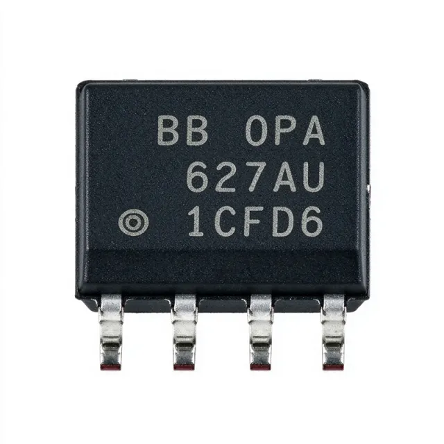
OPA627AU/2K5 - 16MHz Precision JFET Op Amp 55V/us | TI
The Texas Instruments OPA627AU/2K5 is a precision, high-speed JFET-input operational amplifier delivering 16 MHz unity-gain bandwidth, 55 V/us slew rate, and a maximum offset voltage drift of 0.8 uV/C, housed in an 8-pin SOIC (D) package rated for -25C to +85C operation. A JFET-input operational amplifier is a voltage-feedback amplifier whose input stage uses junction field-effect transistors to achieve extremely low input bias current and high input impedance. Within the signal-chain hierarchy, it sits under the operational amplifier family, itself a core analog building block of amplifier ICs and precision analog front-end design. Key features include a very low offset voltage of 100 uV max, maximum drift of 0.8 uV/C, and input bias current as low as 5 pA max thanks to the DiFet (dielectrically isolated FET) input stage. The part is unity-gain stable, settling fast to 0.01% accuracy, and provides very low voltage noise at 10 kHz. Supply operation spans +-4.5 V to +-18 V, supporting both +-15 V industrial analog rails and +-5 V precision systems. Technically, the OPA6x7 family is fabricated on a high-speed dielectrically isolated (DiFet) process, which gives the OPA627 lower noise, lower offset, and higher speed than the earlier OPA111 while retaining picoampere input currents. The sibling OPA637 shares the die but is stable only at gains of 5 or greater, trading stability margins for wider bandwidth at high gain. Typical applications include precision data-acquisition front ends, photodiode transimpedance amplifiers, professional and audiophile audio preamplifiers, and test-and-measurement instrumentation where low offset drift and low bias current are decisive. A key design consideration: because the part is unity-gain stable at 16 MHz, layout with short feedback traces and solid ground planes is essential to avoid parasitic ringing; for gains of 5 or more, the faster OPA637 is often the better choice. This page synthesizes distributor pricing, drop-in alternatives, and practical design notes not found in the manufacturer datasheet.

OPA627BP - 16MHz Precision Difet Op-Amp | Texas Instruments
The Texas Instruments OPA627BP is a precision high-speed Difet (dielectrically isolated FET) operational amplifier delivering 16 MHz unity-gain bandwidth, 55 V/us slew rate, and 0.8 uV/C maximum offset-voltage drift, housed in an 8-pin plastic DIP (PDIP-8) package. A precision operational amplifier is an op-amp engineered to minimize DC error terms - input offset voltage, bias current, and drift - while maintaining usable AC performance. Within the signal-chain hierarchy, it sits between general-purpose amplifiers and instrumentation amplifiers, and the OPA627 belongs to TI's (originally Burr-Brown) Difet family, where dielectric isolation of JFETs dramatically reduces input capacitance and leakage compared to conventional junction-isolated processes. Key differentiating features include the combination of high speed (16 MHz, 55 V/us) with true precision DC accuracy, JFET input for extremely low bias current, and industrial temperature grade options. The 'B' grade suffix denotes tighter offset and drift limits; the 'P' suffix denotes the plastic 8-pin DIP package. Architecturally, the Difet process places a dielectric layer around FET structures, yielding low input capacitance and low input bias current that remain stable over temperature. This is why the OPA627 achieves sub-microvolt-per-degree drift together with wideband dynamics - a combination rarely met by CMOS or bipolar alternatives of its era. Typical applications include high-fidelity audio preamplifiers and headphone amplifiers, precision integrators and photodiode transimpedance stages, active filters, and data-acquisition front ends where both DC accuracy and 16 MHz bandwidth are required. Design consideration: to preserve stability, follow the datasheet layout guidance - keep feedback resistance values moderate and decouple supplies close to pins 4 and 7; the decompensated sibling OPA637 (minimum stable gain of 5) is not a unity-gain-stable substitute. This page synthesizes distributor pricing, drop-in alternative analysis, and practical design notes not consolidated in the manufacturer datasheet, with prices as of 2026-09-13.

OPA627SM - Precision JFET Op Amp 55V/us TO-99-8 | TI
The Texas Instruments OPA627SM is a precision, high-speed JFET-input operational amplifier delivering 55 V/us slew rate, 0.8 uV/C maximum offset drift, and 16 MHz unity-gain bandwidth in an 8-pin TO-99 metal can package rated for ±18 V (36 V) supplies. A low-dropout linear regulator is a voltage regulator; an operational amplifier is an analog signal-chain building block that amplifies the voltage difference between two inputs, sitting within the broader hierarchy of amplifier ICs inside precision analog front ends. The OPA627 family is fabricated on a high-speed dielectrically isolated (DI) process, which separates the JFET input stage from the output stage and enables a rare combination of precision DC accuracy and 55 V/us speed: maximum offset voltage of 100 uV, input bias current of a few picoamperes, and low noise of 4.5 nV/sqrt(Hz) at 1 kHz. Compared with the older OPA111, the OPA6x7 family offers lower noise, lower offset, and significantly higher speed. Key differentiating specifications include the 0.8 uV/C max drift (which eliminates calibration in precision gain stages), 55 V/us slew rate for wide-dynamic-range AC signals, and 16 MHz gain-bandwidth product with unity-gain stability. The SM grade denotes TI's premium grade in the metal can package with tightened limits for offset and drift. Typical applications include precision photo-diode and integrator amplifiers, DAC output I/V conversion, professional and high-end audio preamplifiers, and test-and-measurement signal conditioning where a fast-settling, low-offset JFET amplifier is required. Design consideration: as a JFET op amp, bias current doubles roughly every 10 C, so thermal management of surrounding circuitry matters at high accuracy targets; TI recommends a compensating network and proper decoupling per the datasheet. This page synthesizes distributor pricing, drop-in same-package alternatives, pinout data, and practical design notes not found in the manufacturer datasheet.

OPA631U - 80V 100V/us Single-Supply Op Amp | Texas Instruments
The Texas Instruments OPA631U is a low-power, single-supply operational amplifier featuring high bandwidth, a 100 V/us slew rate, 6 mA supply current, 6 nV/sqrt(Hz) input-voltage noise, operation to +10 V, and an 8-SOIC package. It is designed for instrumentation and signal-conditioning circuits that require fast response from a low-voltage supply. An operational amplifier is an analog integrated circuit that amplifies the voltage difference between two inputs while using negative feedback to set a stable closed-loop gain. The OPA631 belongs to the voltage-feedback operational-amplifier hierarchy, combining low input noise, wide bandwidth, single-supply operation, and rail-adjacent input capability. These characteristics place it between general-purpose amplifiers and higher-speed precision signal-conditioning devices. The verified manufacturer material highlights several performance features: high bandwidth, low 6 mA supply current, operation to +10 V, an input range that includes ground, approximately 4.8 V output swing from a +5 V supply, 100 V/us slew rate, and 6 nV/sqrt(Hz) low input-voltage noise. The zero-power disable function can reduce supply consumption when the amplifier is not needed, although the verified excerpts do not specify its exact shutdown-current value. OPA631U is a voltage-feedback amplifier with one amplifier circuit in an 8-SOIC package. Voltage-feedback topology responds directly to differential input voltage and is suitable for general-purpose gain, filtering, buffering, and instrumentation circuits. Its fast slew rate supports larger signal transitions, while low input voltage noise benefits applications in which source resistance and amplifier noise determine the usable signal floor. Typical uses include low-voltage sensor conditioning, audio and communication signal paths, analog measurement front ends, active filtering, and low-power instrumentation. When using it on a single supply, verify the selected gain, input range, output swing, load, and stability network against the complete manufacturer datasheet. Input and output behavior near the supply rails must be checked at the actual signal amplitude and frequency. For PCB implementation, place the feedback network, decoupling capacitors, and input components close to the amplifier pins. Use a ground plane and minimize parasitic capacitance on high-impedance nodes. This page combines the verified distributor identification, manufacturer-family excerpts, packaging information, and design guidance while identifying parameters that require confirmation from the complete datasheet. The practical design decision is whether the OPA631 speed and noise combination matches the required bandwidth without exceeding power or output-swing limits. Engineers should compare the complete electrical tables, pinout, and package details before production release, especially where input signals approach ground or the output approaches the supply rails.
OPA632U - 68MHz, 6mA Op Amp Single-Supply SOIC-8 | Texas Instruments
The Texas Instruments OPA632U is a SpeedPlus low-power, single-supply operational amplifier featuring 68 MHz bandwidth, 100 V/us slew rate, and 6 mA supply current in an 8-pin SOIC package. The device includes a zero-power disable mode and is designed for single-supply operation from +2.5 V to +10 V (or +/-5 V dual), with input common-mode range that includes ground and a 4.8 V output swing on a +5 V rail, making it suitable for ADC-driver and active-filter signal chains. An operational amplifier (op amp) is a high-gain DC-coupled electronic voltage amplifier with differential inputs and a single-ended output. Within the broader taxonomy, the OPA632 belongs to the voltage-feedback amplifier (VFA) family, which sits under the linear amplifier IC class, which in turn is a sub-category of analog signal-conditioning integrated circuits. The OPA632's distinguishing feature versus general-purpose op amps is its combination of wide bandwidth, high slew rate, and low input voltage noise (6 nV/sqrt(Hz)) in a power-efficient package. Key features of the OPA632U include 68 MHz unity-gain bandwidth, 100 V/us slew rate, 6 nV/sqrt(Hz) input-referenced voltage noise density, a low 6 mA quiescent current, and an integrated shutdown pin for power saving. The amplifier is unity-gain stable and provides a rail-to-rail output swing that approaches the positive rail and includes ground at the negative input range, easing single-supply signal chain design. Internally, the OPA632 uses a complementary bipolar architecture with a proprietary input stage that achieves low input bias current while preserving high bandwidth. The architecture delivers low distortion (typically 0.02 percent THD+N at 1 kHz into 600 ohm loads) and excellent DC precision, with a typical input offset voltage of +/-1 mV. The 8-pin SOIC (D) package is pin-compatible with industry-standard single op amp footprints, allowing drop-in replacement in existing designs. Typical applications of the OPA632U include high-fidelity audio ADC input buffers, active filter blocks, photodiode transimpedance front-ends, professional audio line drivers, and portable instrumentation. In each case, the combination of 68 MHz bandwidth, 6 mA supply current, and shutdown support makes the OPA632 a flexible analog building block for cost-sensitive but performance-critical designs. When designing with the OPA632U, observe the maximum supply rating of +12 V (or +/-6 V dual) and ensure output loading remains within the datasheet's safe operating area. Decouple the supply pin with a 0.1 uF ceramic capacitor placed within 5 mm of the IC, and use low-ESR bulk capacitance if the supply traces exceed 25 mm. The enable/disable pin should be tied to the positive supply through a 10 kohm resistor if the shutdown feature is not used, to prevent floating-input noise on that pin.
OPA634U - Wideband Single-Supply Op Amp | Texas Instruments
The Texas Instruments OPA634U is a wideband, single-supply operational amplifier from TI's SpeedPlus family, housed in an 8-pin SOIC package. It is a voltage-feedback amplifier with approximately 200 MHz bandwidth, 250 V/us slew rate, and 5.6 nV/sqrt(Hz) input voltage noise, designed for high-speed signal-chain applications on low-voltage rails. The OPA634U operates from a single +5V supply, swings 4.8V on +5V, and supports a ground-referenced input range that includes 0V, simplifying single-supply ADC interface designs. A wideband, single-supply operational amplifier is a type of analog integrated circuit that combines high small-signal bandwidth with the ability to operate from a single low-voltage rail (typically 3V or 5V), eliminating the need for symmetrical plus/minus supplies. Wideband amplifiers sit in the signal-chain hierarchy between general-purpose op-amps and dedicated RF gain blocks: they are faster than audio op-amps but lower in distortion and noise than full RF amplifiers. This makes them ideal for intermediate-frequency (IF) stages, video drivers, and high-speed transducer signal conditioning where rail-to-rail input and wide output swing are required simultaneously. Key features include 200 MHz unity-gain bandwidth, 250 V/us slew rate, 5.6 nV/sqrt(Hz) input voltage noise density, 80 mA output current capability, and disable-free continuous operation. The architecture is a current-feedback topology optimized for low quiescent current while preserving large-signal behavior, allowing the OPA634U to drive 150 ohm loads to within 1V of either rail. The SOIC-8 package provides a familiar pinout and wide compatibility with hand-soldering and standard SMT assembly lines. The internal design uses TI's high-speed complementary bipolar process, with a proprietary input stage that accepts signals from below ground to within 1.5V of the positive rail. This makes the OPA634U particularly effective as a single-to-differential buffer for high-speed ADCs, an active filter for IF stages, and a low-distribution pre-amplifier for video and instrumentation front-ends. Its wide bandwidth and high output drive also suit line-driver applications in industrial and broadcast video distribution. Typical applications include high-speed single-to-differential ADC drivers, IF/RF signal-chain buffers, video line drivers, active filter implementations, transducer signal conditioning, and portable test equipment signal paths. The wide bandwidth and high slew rate make it especially well suited to applications up to 10 MHz where pulse fidelity and settling time are critical. When designing with the OPA634U, take care to provide low-impedance source termination for current-feedback stability - the datasheet's recommended feedback resistor of 750 ohms at G=+2 should be respected. Decouple the +5V supply with a 0.1 uF ceramic placed within 5 mm of the supply pin and a 4.7 uF tantalum or ceramic bulk cap on the board-level rail. Avoid running the output trace near sensitive analog inputs to minimize crosstalk, and keep the inverting input trace short to preserve the high-frequency feedback loop. This page synthesizes distributor pricing, drop-in alternatives, and practical design notes not found in the manufacturer datasheet.
OPA635U - 100MHz High-Speed Amplifier | Texas Instruments
The Texas Instruments OPA635U is a single-circuit, voltage-feedback operational amplifier optimized for high-speed signal conditioning on supplies up to +10 V. Its three headline characteristics are 100 MHz gain-bandwidth product, 250 V/us slew rate, and 5.6 nV/sqrt(Hz) input-voltage noise, all supplied in an 8-pin SOIC package. The OPA635U also provides a shutdown function, an input range that includes ground, 4.8 V output swing from a +5 V supply, and output-current capability up to 80 mA. A high-speed operational amplifier is a voltage-feedback amplifier designed to amplify rapidly changing signals while maintaining useful gain, bandwidth, slew rate, and signal integrity. Within the broader hierarchy, an operational amplifier is an analog IC, and the OPA635U belongs to the high-speed voltage-feedback amplifier family. Its SpeedPlus architecture targets circuits requiring wide bandwidth and fast large-signal response without relying on a complex external compensation network. Key features include bandwidth extending to 100 MHz under the stated gain condition, 250 V/us slew rate, and 5.6 nV/sqrt(Hz) low input-voltage noise. The device supports operation to +10 V, can drive 80 mA, and can be placed in a shutdown state when the OPA635 version's power-disable function is used. Its input range extends to ground, making it relevant to single-supply systems that process signals near 0 V. The combination of high bandwidth and slew rate is useful in video and test equipment, high-speed filters, communications interfaces, active impedance conversion, and instrumentation buffers. Low input noise is especially relevant when amplifying small signals, while the 80 mA output-current capability provides drive for downstream stages and termination networks. Actual gain bandwidth, stability, and output swing depend on the selected gain, supply voltage, load, and feedback network. For +5 V operation, the verified data identifies a 4.8 V output swing, which leaves less headroom than the full supply rail and should be considered when designing receiver or driver interfaces. The 250 V/us slew rate supports fast transitions, but board parasitics, capacitive loading, and feedback-loop stability remain critical at high frequency. The SOIC package helps preserve the amplifier's high-frequency behavior compared with larger parasitic packages. A practical design should use short, controlled-impedance traces, a small, symmetric feedback network, and decoupling close to the supply pins. If the application does not need shutdown, the disable function should be tied to its inactive level according to the manufacturer datasheet. Confirm stability and output swing on the completed PCB because high-speed amplifier performance is sensitive to loading, grounding, and component placement. This page consolidates the verified OPA635U features, source links, package information, design cautions, and replacement-status assessment. It is intended to help engineers locate the datasheet, understand the core electrical limits, and plan a replacement without assuming that merely similar amplifier specifications guarantee drop-in compatibility.
OPA637AM - Precision High-Speed DiFET Op Amp | Texas Instruments
The Texas Instruments OPA637AM is a precision high-speed DiFET (dielectrically isolated FET) operational amplifier supplied in a TO-99-8 metal can package, featuring a maximum input offset voltage of 100 uV, a maximum offset drift of 0.8 uV/C, and a maximum input bias current of 5 pA. Unlike its unity-gain-stable sibling OPA627, the OPA637 is de-compensated and stable only at closed-loop gains of 5 or greater, which enables significantly higher bandwidth in high-gain configurations. An operational amplifier is a high-gain DC-coupled voltage amplifier with differential inputs and a single-ended output, forming the foundational building block of the analog signal chain hierarchy: op amp -> amplifier IC -> analog IC -> semiconductor. Precision high-speed op amps such as the OPA637 combine the low input bias current of a JFET-input (DiFET) process with the speed required for fast-settling data acquisition systems. Key differentiating features include very low noise at 10 kHz, a fast settling time to 0.01% accuracy, low offset voltage (100 uV max), and extremely low bias current (5 pA max) enabled by the DiFET process. The metal TO-99-8 can provides superior EMI shielding and thermal performance compared to plastic packages. The DiFET architecture uses dielectrically isolated FET input transistors on a bipolar process, achieving both precision DC accuracy and wideband AC performance. The de-compensated internal design removes the internal compensation capacitor overhead, delivering higher slew rate and gain-bandwidth at gains above 5. Typical applications include high-speed data acquisition, precision pulse amplification, photodiode transimpedance amplification at high gain, and professional audio and instrumentation signal chains where low noise and fast settling are both required. Design consideration: because the OPA637 is only stable at gains of 5 or above, do not use it in unity-gain buffer configurations; choose the pin-compatible OPA627AM instead for gain-of-1 applications. This page synthesizes distributor pricing, drop-in alternatives, design notes, and application guidance not found in the manufacturer datasheet.
OPA637AP - 80MHz Precision Difet Op Amp DIP-8 | Texas Instruments
The Texas Instruments OPA637AP is a precision high-speed Difet (dielectrically isolated FET) operational amplifier delivering 80 MHz unity-gain bandwidth and 135 V/us slew rate, supplied in an 8-pin PDIP package and operating from dual supplies of +/-4.5V to +/-18V. A high-speed operational amplifier is a voltage-feedback amplifier designed to combine wide bandwidth with DC precision, sitting within the hierarchy: op-amp -> precision amplifier -> analog signal conditioning IC -> semiconductor. Where general-purpose amplifiers trade speed for accuracy, precision high-speed parts like the OPA637 preserve both, enabling high-dynamic-range analog signal chains. Key features of the OPA637AP include a very low maximum offset voltage of 100 uV, a maximum offset drift of 0.8 uV/C, and a maximum input bias current of only 5 pA thanks to the Difet (dielectrically isolated FET) input process. The amplifier settles fast to 0.01% accuracy and is unity-gain bandwidth specified at 80 MHz. Unlike its sibling OPA627, which is unity-gain stable, the OPA637 is stable only at closed-loop gains of 5 or greater - the compensation scheme de-compensates the amplifier to achieve its higher bandwidth, which is why the 80 MHz figure exceeds the OPA627's. The Difet process uses dielectric isolation rather than junction isolation, sharply reducing input capacitance and leakage. This yields the picoampere-class bias current and low noise typically associated with JFET-input precision amplifiers while preserving the high slew rate needed for fast pulse and wideband AC signals. Typical applications include wideband data-acquisition front ends, fast pulse amplification in test and measurement instruments, photodiode transimpedance stages with high closed-loop gain, and active filters in precision instrumentation. A key design consideration: because the OPA637 requires a minimum closed-loop gain of 5 for stability, do not substitute it for the unity-gain-stable OPA627 in follower configurations. Verify noise-gain margins and use good high-frequency PCB layout with short feedback paths. This page synthesizes distributor pricing, drop-in alternatives, pinout data, and practical design notes not found in the manufacturer datasheet.

OPA637AU - Precision High-Speed Difet Op Amp | TI | Gain ≥5
The Texas Instruments OPA637AU is a precision high-speed Difet (dielectrically isolated FET) operational amplifier delivering 16 MHz bandwidth, 100 uV maximum input offset voltage, and 5 pA maximum input bias current in an 8-pin SOIC (D) package. Unlike its unity-gain-stable sibling OPA627, the OPA637 is decompensated and stable only at closed-loop gains of 5 or greater, which allows roughly twice the bandwidth and slew rate of the OPA627 in the same silicon. An operational amplifier is a high-gain differential voltage amplifier that forms the core building block of analog signal chains. Within the amplifier hierarchy, precision JFET-input and Difet op-amps occupy the segment between general-purpose bipolar amplifiers and ultra-fast current-feedback parts, combining very low input bias current with high speed and low noise. The Difet process uses dielectric isolation to reduce junction capacitances, enabling the OPA637's speed without sacrificing the picoampere-level bias current characteristic of JFET inputs. Key differentiating features include very low input voltage noise at 10 kHz, fast settling to 0.01% accuracy, maximum input offset voltage of 100 uV, and maximum offset drift of 0.8 uV/C. These parameters matter directly in precision measurement front ends, where offset error and drift accumulate as systematic error, and in wideband stages where noise sets the achievable dynamic range. Laser trimming of the input stage achieves the tight offset specification. Technically, the decompensated internal compensation capacitor is sized for a minimum noise gain of 5, trading phase margin at low gains for extended bandwidth and slew rate in high-gain configurations. This makes the part well suited to I/V conversion from photodiodes, gain-of-5 and higher instrumentation amplifier input stages, active filters, and DAC output buffering in high-resolution systems. Typical applications include precision data acquisition front ends, photodiode transimpedance amplifiers, professional audio equipment, and test and measurement instrumentation. The pA-level bias current preserves accuracy with high-impedance sources, while the 16 MHz-class bandwidth supports fast settling after transients. A critical design consideration: never use the OPA637 at closed-loop gains below 5, as it will oscillate; choose the pin-compatible OPA627 in the same SOIC-8 footprint for unity-gain applications. Proper supply decoupling with 0.1 uF ceramic capacitors at both rails is essential at these speeds. This page synthesizes distributor pricing, drop-in alternatives, and practical design notes not found in the manufacturer datasheet, with verified data as of 2026-09-13.
OPA637AU/2K5 - 80MHz Precision Difet Op-Amp | TI
The Texas Instruments OPA637AU/2K5 is a precision high-speed Difet (dielectrically isolated JFET) operational amplifier delivering 80 MHz bandwidth and 135 V/µs slew rate in an 8-pin SOIC (D) package, supplied in tape-and-reel packaging with 2500 units per reel. A precision high-speed operational amplifier is a voltage-feedback amplifier that combines wide signal bandwidth with DC accuracy specifications normally reserved for precision instrumentation amplifiers. Within the amplifier hierarchy, the OPA637 sits in the precision JFET-input family: operational amplifier -> high-speed amplifier -> Difet precision op-amp -> signal conditioning IC. Its dielectrically isolated (Difet) JFET process achieves speed without sacrificing the low input bias current that JFET inputs provide. Key features include very low input noise at 10 kHz, fast settling to 0.01%, low offset voltage (100 µV max for the A grade), low drift (0.8 µV/°C max), and extremely low input bias current (5 pA max). The supply range spans ±4.5 V to ±18 V, allowing operation on standard ±15 V analog rails. Technically, the OPA637 is decompensated: unlike its unity-gain-stable sibling OPA627, the OPA637 is stable only in closed-loop gains of 5 or greater. This internal compensation trade-off is exactly what enables the 80 MHz bandwidth and 135 V/µs slew rate; at gain ≥5 it outpaces unity-gain-stable competitors while retaining Difet DC precision. Typical applications include photodiode transimpedance amplifiers with high closed-loop gain, fast precision data-acquisition front ends, video and broadband signal conditioning, and DAC output I/V conversion where both speed and sub-millivolt DC accuracy matter. Design consideration: verify every circuit using the OPA637 operates at closed-loop gain ≥5; substituting it directly for a unity-gain-stable op-amp (such as the OPA627 in the same package) will cause oscillation. This page synthesizes verified distributor pricing, drop-in alternatives within the OPA637 family, and design notes not found in the manufacturer datasheet.
OPA637BP - 80MHz Precision Difet Op Amp DIP-8 | Texas Instruments
The Texas Instruments OPA637BP is a precision high-speed Difet (dielectrically isolated FET) operational amplifier delivering an 80 MHz unity-gain crossover and a 135 V/us slew rate, powered from supplies of plus/minus 4.5 V to plus/minus 18 V in an 8-pin PDIP (DIP-8) package. An operational amplifier (op amp) is a high-gain voltage amplifier with differential inputs and a single-ended output that, with external feedback networks, forms the basis of amplifiers, filters, integrators, buffers, and precision signal-conditioning stages within the broader hierarchy of analog signal-chain ICs. JFET-input and Difet-process op amps combine the low input bias current of field-effect inputs with the speed of dielectrically isolated bipolar processes, occupying a niche between general-purpose CMOS and fully bipolar high-speed amplifiers. Key features of the OPA637BP include very low input offset voltage of 100 uV maximum, offset drift of 0.8 uV/C maximum, and input bias current of 5 pA maximum - values enabled by the JFET input stage. Compared to the popular OPA111, the OPA6x7 family offers lower noise, lower offset, and higher speed. The B-grade OPA637BP provides tighter precision than the A-grade OPA637AP. Technically, the OPA637 is fabricated on a high-speed dielectrically isolated complementary NPN/PNP (Difet) process. Critically, it is decompensated: unlike the unity-gain-stable OPA627, the OPA637 is stable only at closed-loop gains of 5 or greater, which permits its higher bandwidth and slew rate. Designs using the OPA637 in gain below 5 will oscillate. Typical applications include precision ADC/DAC buffering and I/V conversion, photodiode transimpedance amplifiers, high-speed data-acquisition front ends, and professional audio and test instrumentation stages where gain is configured at 5 or higher. Design consideration: verify the noise-gain of your topology is at least 5 V/V; for unity-gain buffering use the OPA627 instead. Also respect the 135 V/us slew rate when driving large signals to avoid distortion from slew limiting. This page adds distributor pricing tiers, pin-compatible alternatives, comparison tables, and practical design notes not found in the manufacturer datasheet.

OPA640P - 1.3 GHz Wideband Op Amp | Texas Instruments
The Texas Instruments OPA640P is a single-circuit, unity-gain-stable voltage-feedback operational amplifier with a 1.3 GHz unity-gain bandwidth, 2.9 nV/√Hz input noise, 350 V/µs slew rate, and 85 dB common-mode rejection ratio. The device is supplied in an 8-pin PDIP package, making it suitable for through-hole instrumentation, communications, video, and wideband signal-chain designs. An operational amplifier is a voltage-feedback amplifier that uses high open-loop gain to amplify the voltage difference between its inverting and non-inverting inputs. Within the broader semiconductor hierarchy, the OPA640P is an analog linear IC, an operational amplifier, and a wideband voltage-feedback amplifier. Its combination of bandwidth, slew rate, and low noise distinguishes it from general-purpose precision amplifiers intended mainly for slow signal conditioning. The OPA640P's 1.3 GHz unity-gain bandwidth supports wide closed-loop bandwidth when the surrounding feedback network permits it. Unity-gain stability means the amplifier can provide useful closed-loop operation without requiring a high noise-gain setting. Its 350 V/µs slew rate supports rapid signal transitions, while the specified 2.9 nV/√Hz noise density supports high-gain amplification of low-level analog signals. The verified source material also identifies 85 dB common-mode rejection and emphasizes low harmonic distortion at 10 MHz. These characteristics matter when the amplifier processes small signals superimposed on larger common-mode voltages or when broadband nonlinear distortion would limit measurement accuracy. The OPA640P is a voltage-feedback device rather than a current-feedback amplifier, so its feedback network and stability behavior should be evaluated using the manufacturer's guidance. Typical applications include broadband instrumentation, communications-interface signal conditioning, video amplification, active filtering, buffer stages, and gain blocks requiring more bandwidth than ordinary precision op amps provide. The wide operating capability can help designers preserve signal fidelity when analog stages must operate over a substantially higher frequency range than conventional audio-frequency amplifiers. Designers should confirm the complete electrical limits, recommended supply voltages, common-mode range, output swing, input bias current, offset voltage, and stability network requirements in the manufacturer datasheet before production use. Because the verified excerpts do not provide the complete pin mapping or application circuit values, those details must not be inferred from the package description alone. This page combines verified distributor information, distributor availability context, and manufacturer-style technical parameters for OPA640P selection. It also identifies where additional engineering data is required rather than presenting unverified specifications, ensuring that bandwidth, noise, slew-rate, packaging, and lifecycle decisions can be traced to available source material.
OPA643P - Wideband Low-Distortion Op Amp | Texas Instruments
The Texas Instruments OPA643P is a wideband, low-distortion, high-gain monolithic operational amplifier from the Burr-Brown product line, configured as a single-channel voltage-feedback amplifier in an 8-pin PDIP through-hole package. The device delivers a gain-bandwidth product of 800 MHz, a 1000 V/µs slew rate, an ultra-low input voltage noise of 2.3 nV/√Hz, and low harmonic distortion of 5 MHz, making it well-suited for high-frequency signal conditioning where both speed and noise floor matter. A voltage-feedback operational amplifier is an analog active device that amplifies the difference between two input voltages while presenting a high input impedance and a low output impedance. The "voltage-feedback" architecture (as opposed to current-feedback) is characterized by a constant gain-bandwidth product, meaning that as closed-loop gain increases, usable bandwidth decreases proportionally. This topology sits within the broader hierarchy: operational amplifier -> analog amplifier -> amplifier IC -> integrated circuit -> semiconductor. The "P" suffix in the OPA643P designation specifically identifies the PDIP-8 plastic through-hole package, distinguishing it from surface-mount variants such as the OPA643N (SOIC-8) and OPA643U (SOT-23-5). Key features include low distortion specified at 5 MHz, 2.3 nV/√Hz input voltage noise density, 800 MHz gain-bandwidth product, 1000 V/µs slew rate, and stability for gains of 3 or higher. The wide supply range of ±5.5 V (11 V total) makes the device compatible with typical ±5 V analog rails. Its high open-loop gain and excellent DC precision support demanding instrumentation applications that require both wideband AC performance and accurate low-frequency operation. The OPA643P is built on a high-speed complementary bipolar process, which is the underlying technology enabling the combination of high slew rate, low noise, and low distortion. The internal topology is fully compensated for unity-gain stability, and external feedback components set the closed-loop response. Designers can exploit the high gain-bandwidth product for wideband transimpedance and ADC-driver applications, while the low-distortion characteristic suits communications IF stages, video buffers, and high-fidelity audio line drivers. Typical applications include wideband instrumentation amplifiers, low-distortion ADC input buffers, high-speed line drivers, video amplifier stages, communications IF amplifier blocks, and active filters. The device is also frequently deployed in test and measurement front-ends, medical imaging analog front-ends, and high-speed transimpedance amplifiers for photodiode interfaces. When designing with the OPA643P, attention to PCB layout is critical because the 800 MHz gain-bandwidth product makes the circuit susceptible to parasitic capacitance, ground bounce, and supply-rail ringing. Use a solid ground plane, short input traces, and well-bypassed supply pins (typically 0.1 µF ceramic in parallel with 6.8 µF tantalum) to preserve the datasheet's distortion and noise performance in practice. This page synthesizes distributor pricing, drop-in same-package alternatives, and practical design notes not found in the manufacturer datasheet alone.
OPA643U - 800MHz High-Gain Op Amp | Texas Instruments
The Texas Instruments OPA643U is a wideband, low-distortion, high-gain operational amplifier featuring an 800 MHz gain-bandwidth product, 1000 V/µs high slew rate, 2.3 nV/√Hz low noise, and 5 MHz low-distortion operation in an 8-pin SOIC package. It is stable at gains of 3 or greater and is designed for high-speed signal conditioning, active filtering, video, communications, and test equipment. An operational amplifier is an analog integrated circuit that amplifies the voltage difference between its differential inputs. A voltage-feedback operational amplifier falls within the broader hierarchy of amplifier ICs, analog signal-chain ICs, and semiconductor devices. The OPA643U uses a de-compensated voltage-feedback architecture with two internal gain stages, allowing it to maintain high speed and dynamic range at relatively high closed-loop gains. Key features include an 800 MHz gain-bandwidth product for high closed-loop bandwidth, a 1000 V/µs slew rate for rapid large-signal transitions, and 2.3 nV/√Hz input noise for sensitivity in wideband circuits. The device is stable in gains of 3 and above, which supports gain settings that are higher than those normally used with unity-gain-stable amplifiers. It is available in an 8-pin SOIC package. The de-compensated architecture is important because it reserves performance for applications operating at higher closed-loop gains instead of simply providing maximum bandwidth near unity gain. However, feedback-network design remains critical: resistor and capacitor values, parasitic capacitance, and trace geometry can alter effective gain, peaking, and stability. Designers should follow the manufacturer datasheet for recommended gain and feedback arrangements rather than treating the amplifier as a unity-gain-stable part. Typical applications include broadband analog filtering, video signal conditioning, communications receivers, instrumentation, and high-speed test-equipment input stages. It is particularly useful where the required signal bandwidth is high and the circuit operates with a closed-loop gain of at least 3. For applications involving ADC drivers, cable termination, or impedance-sensitive analog nodes, the complete signal path must be evaluated for noise, output drive, and parasitic effects. A primary design consideration is stability at the intended gain and noise bandwidth. Keep feedback loops short, use the package ground and power pins as specified, and provide adequate high-frequency bypassing with low-inductance placement. The verified distributor excerpts identify the SOT23-5 package option for the device family, while OPA643U orderable-package information identifies an 8-pin SOIC package. This page consolidates verified manufacturer and distributor excerpts, exact available parameters, sourcing links, application guidance, and engineering constraints. It also distinguishes documented OPA643U attributes from data that still requires confirmation from the complete datasheet or an authorized distributor before production release.
OPA644U - 500MHz Current-Feedback Op Amp | Texas Instruments
The Texas Instruments OPA644U is a low-distortion current-feedback operational amplifier with 500 MHz bandwidth, a 2500 V/µs slew rate, and very low differential gain and phase error in an 8-pin SOIC package. The device is intended for wideband signal chains that require high bandwidth, rapid slew response, low distortion, and accurate amplitude and phase behavior. A current-feedback operational amplifier is a voltage-input, voltage-output amplifier whose feedback impedance establishes the closed-loop gain. It belongs to the operational-amplifier hierarchy within analog and mixed-signal ICs. Unlike a voltage-feedback amplifier, the OPA644U is optimized for high-speed applications in which gain bandwidth, output-drive capability, slew rate, and feedback-component selection strongly influence signal fidelity. Principal features include 2500 V/µs slew rate, 0.008% differential gain error, 0.009° differential phase error, -85 dBc low distortion, 500 MHz bandwidth, and a 2.0 MΩ open-loop transimpedance. The amplifier is unity-gain stable and supports fast 12-bit settling to 0.01%. These characteristics make it suitable for wideband analog signal conditioning, data-conversion interfaces, video, communications, instrumentation, and test equipment. OPA644U uses a current-feedback topology whose closed-loop response depends on the external feedback resistor and termination network. High bandwidth and slew rate provide rapid signal transitions, while the specified low differential gain and phase error support accurate amplification of high-frequency waveforms. Designers should still validate stability, bandwidth, output swing, and distortion against their actual gain, load, supply, and feedback configuration. Typical applications include video distribution, high-speed instrumentation, communications receivers, analog-to-digital and digital-to-analog converter interfaces, active filters, and wideband test equipment. The 8-pin SOIC package makes the device suitable for conventional surface-mount assembly, although high-speed layouts require short traces, controlled impedance, and careful decoupling. The main design consideration is feedback-network compatibility. Current-feedback amplifiers require resistor values chosen for the target closed-loop gain, and improper feedback impedance can alter bandwidth or induce peaking. Input and output networks should be evaluated experimentally, with supply bypassing placed close to the device pins. This page consolidates verified distributor availability, exact manufacturer characteristics, same-family replacement analysis, and practical high-speed layout guidance to support faster component selection and safer PCB implementation.
OPA646U - Low-Power Wide-Bandwidth Op Amp | Texas Instruments
Texas Instruments OPA646U is a low-power, wide-bandwidth, single-circuit voltage-feedback operational amplifier packaged in an 8-pin SOIC. The verified distributor listing identifies it as a voltage-feedback amplifier with one amplifier circuit per package, while the archived manufacturer datasheet describes the OPA646 family as a low-power, wide-bandwidth operational amplifier. Its SOIC-8 package supports conventional surface-mount assembly and is identified consistently by the distributor sources. An operational amplifier is a voltage-controlled, high-gain analog building block used to amplify differential signals, buffer sensors, drive analog stages, and implement active filters. The voltage-feedback architecture belongs to the operational-amplifier family within analog signal-chain and semiconductor product hierarchies. Unlike a comparator, the OPA646U is intended for continuous linear signal amplification, although its exact input common-mode range, output swing, and stable gain range must be confirmed in the manufacturer datasheet. The principal verified features are low power consumption, wide bandwidth, voltage-feedback operation, one amplifier circuit per package, and an 8-pin SOIC format. These characteristics make the OPA646U relevant to precision signal-conditioning paths where an amplifier must combine modest power use with higher-frequency capability. Exact gain-bandwidth product, slew rate, input noise, offset voltage, and supply-current figures were not included in the supplied source data and therefore are not inferred here. The device can be considered for instrumentation, communications, industrial measurement, audio, and data-acquisition systems. Its voltage-feedback topology is generally suitable for closed-loop gain configurations when the selected noise gain, signal amplitude, output loading, and supply voltage remain within the manufacturer’s specified operating limits. Because the retrieved snippets do not provide complete electrical ratings, these limits must be checked before final circuit release. A practical design review should verify supply range, input common-mode range, output swing, capacitive-load stability, noise-gain headroom, and power dissipation against the full OPA646 datasheet. Decoupling capacitors, grounding, signal routing, and output-loading constraints also require confirmation using the manufacturer’s recommended circuit and layout guidance. This page consolidates the verified distributor identity, package, pricing, source links, same-family replacement options, comparison gaps, and practical design guidance into one engineering reference. It deliberately separates confirmed OPA646U facts from parameters that require manufacturer-datasheet verification, helping procurement and design teams avoid unsupported assumptions.
OPA650U - 560 MHz Low-Power Voltage Feedback Op Amp | TI
Texas Instruments OPA650U is a wideband, low-power, single-circuit voltage-feedback operational amplifier with a 560 MHz unity-gain bandwidth, 50 mW power consumption, and low input bias current of 5 µA. The device is supplied in an 8-pin SOIC package and is optimized for high-speed signal conditioning, instrumentation, and analog signal-processing applications. An operational amplifier is an analog integrated circuit that amplifies the voltage difference between its inverting and non-inverting inputs while using negative feedback to set the closed-loop gain. The OPA650U belongs to the voltage-feedback operational amplifier family within the broader amplifier and signal-conditioning IC hierarchy. Unlike a current-feedback amplifier, its gain-bandwidth and stability behavior depend on the applied noise gain and feedback network. Key features include a 560 MHz unity-gain bandwidth, 50 mW power dissipation, low harmonic distortion characterized at 5 MHz, fast settling to 0.01%, and input bias current of 5 µA. The unity-gain-stable configuration allows it to operate directly as a buffer without requiring a higher minimum gain. Its wide bandwidth makes it suitable for fast instrumentation, low-level signal conditioning, test equipment, and communications signal paths. OPA650U uses a voltage-feedback architecture and is available in the 8-SOIC package identified by distributor listings as a single, wideband voltage-feedback amplifier. The verified sources describe it as the OPA650 family device for wideband, low-power operation. Exact supply-voltage limits, input and output swing, offset voltage, slew rate, noise density, operating-temperature range, and short-circuit behavior were not included in the retrieved data and must be confirmed in the manufacturer datasheet before design release. Typical uses include high-speed buffer stages, instrumentation front ends, active analog filters, waveform conditioning, communications equipment, laboratory instruments, and data-acquisition systems. When operating at high closed-loop gain, engineers should evaluate noise gain, phase margin, stability, output drive, and component tolerances rather than relying only on the 560 MHz unity-gain figure. The primary design considerations are supply bypassing, feedback-loop stability, output loading, and thermal management. Place the specified input and output network components close to the device, preserve the manufacturer-recommended layout, and avoid long high-impedance traces around the amplifier. A small-signal bandwidth number does not guarantee large-signal settling, and the 50 mW power figure should not be interpreted as a substitute for checking output-current and supply-limit constraints. This page combines the verified manufacturer-family description, distributor availability information, an obsolete-status report, and package-level cross-reference information. It also separates documented facts from unavailable parameters, highlights engineering checks that are absent from basic distributor summaries, and identifies where a true drop-in replacement requires additional validation.
OPA651U - 470MHz Wideband Low-Power Op Amp | Texas Instruments
The Texas Instruments (formerly Burr-Brown) OPA651U is a wideband, low-power, voltage-feedback operational amplifier housed in an 8-pin SOIC (D) package. It delivers 470 MHz small-signal bandwidth at a gain of +2 V/V while consuming only 50 mW of quiescent power from ±5 V supplies, making it one of the highest bandwidth-per-milliwatt parts of its generation. Key headline parameters include 340 V/µs slew rate, 16 ns settling time to 0.01% (12-bit accuracy), 4 µA input bias current, 5 MHz low-harmonic operation, and 0.05%/0.1° differential gain/phase error. The part is unity-gain stable in gains of 2 V/V or higher. What is a voltage-feedback op amp? A voltage-feedback operational amplifier (VFA) is a class of analog amplifier whose differential input pair senses a voltage difference and whose output drives a load through a high-gain internal stage. VFAs sit in the hierarchy: op amp -> amplifier IC -> analog signal chain -> semiconductor. Unlike current-feedback amplifiers (CFAs), VFAs can typically be used in any closed-loop gain configuration, with bandwidth that scales inversely with the closed-loop gain. The OPA651 belongs to the classic wideband VFA family designed for video, ADC driver, and high-speed signal-conditioning roles. Architecturally, the OPA651 uses a complementary bipolar input stage feeding a high-slew-rate gain block, which is why it achieves both low input bias current and a fast 340 V/µs slew rate simultaneously. The voltage-feedback topology gives the designer freedom to set gain with two external resistors while the internal compensation keeps the part stable from a gain of 2 V/V upward. A disable pin (pin 8) on selected grades allows power saving in multi-channel systems. Typical applications include video line drivers, RGB routing, ADC input buffers for 12-bit pipelined converters, ultrasound pre-amplifier stages, active filters, and IF/RF signal-chain blocks where 50 mW dissipation and SO-8 footprint are acceptable. The low input bias current of 4 µA also makes it usable in photodiode transimpedance front-ends when bandwidth and noise trade-offs are managed. When laying out the OPA651, place the feedback and gain-setting resistors as close as possible to the inverting input pin, use a solid low-impedance ground plane, and bypass both supply pins with 0.1 µF ceramics in parallel with 4.7 µF tantalums. For lowest distortion, terminate the input with 50 Ω and keep the output load capacitance below 20 pF. This page synthesizes distributor pricing, drop-in alternative MPNs, and practical PCB design notes that the original 1998-era datasheet does not consolidate in a single place, giving the working engineer a faster path to a vetted BOM entry.
OPA655U - Wideband FET Op Amp, ±5.25 V | Texas Instruments
Texas Instruments OPA655U is a single-circuit, wideband, unity-gain-stable operational amplifier with a FET input and a ±5.25 V supply capability, housed in an 8-pin SOIC package. It is positioned for instrumentation, signal-conditioning, and high-speed analog systems requiring a low-noise input stage with broad operating range. The verified product data identifies the device as a voltage-feedback amplifier, which supports straightforward closed-loop gain implementation and predictable compensation. A voltage-feedback operational amplifier is a transistor-based analog circuit that amplifies the voltage difference between its inverting and non-inverting inputs. The voltage-feedback amplifier family belongs to the broader operational-amplifier hierarchy, analog IC hierarchy, and semiconductor hierarchy. Unlike a current-feedback amplifier, a voltage-feedback amplifier uses internal frequency compensation, allowing it to remain stable at unity gain when configured with suitable feedback and source impedances. The OPA655U provides eight key verified characteristics. It is a wideband amplifier, is stable at a gain of one, uses a FET input, contains one amplifier circuit, accepts a supply specified as ±5.25 V, and is available in an 8-pin SOIC package. The listed temperature grade is industrial, while the package uses a gull-wing surface-mount form. These characteristics make it applicable where a precision input device is required within a modest-size instrumentation circuit. OPA655U belongs to the wideband, low-noise amplifier class rather than the general-purpose precision op-amp class. Its FET input is the defining input-stage technology reported by the manufacturer data, while unity-gain stability supports direct use as a buffer when the application conditions satisfy the amplifier's operating requirements. The 8-SOIC format provides a conventional surface-mount footprint that is also used by several related high-speed amplifier families. Typical uses include photodiode and optical-signal conditioning, waveform monitoring, laboratory instrumentation, communications-interface signal paths, precision feedback networks, and high-speed data-acquisition front ends. In these systems, the amplifier can condition a small differential signal before it reaches an ADC, implement active filtering, or drive a subsequent analog stage when the voltage and current limits of the selected feedback network remain within device specifications. Designers should verify the required supply rails, input common-mode range, output swing, input bias current, noise density, slew rate, gain-bandwidth behavior, and stability conditions directly against the manufacturer datasheet before release. Layout should provide a short, low-impedance feedback path and careful grounding to avoid adding parasitic gain or instability. Component values and timing margins should be derived from the datasheet's tested application circuits rather than inferred solely from the generic amplifier category. This page consolidates the verified distributor and manufacturer information, separates known OPA655U attributes from parameters that still require datasheet confirmation, and documents the only supported drop-in cross-reference found in the supplied replacement search. It also provides purchasing guidance, application fit, comparison boundaries, and practical design checks that help engineers distinguish a genuine replacement from a merely similar amplifier.
OPA656U - 500MHz FET-Input Op Amp | Texas Instruments
The Texas Instruments OPA656U is a single-circuit, wideband, unity-gain-stable, FET-input operational amplifier with a 500 MHz gain-bandwidth product and 290 V/µs slew rate, supplied in an 8-pin SOIC package. It supports dual supply voltages from ±5 V to ±6 V and is intended for high-speed, high-dynamic-range analog signal paths. An operational amplifier is a voltage-feedback amplifier that uses negative feedback to control gain and improve signal fidelity. The OPA656 belongs to the FET-input operational-amplifier family, combining a high-impedance input stage with wideband signal handling. Within the amplifier hierarchy, it is a wideband voltage-feedback operational amplifier, an analog amplifier, and ultimately a semiconductor used to condition, buffer, or amplify analog signals. Key features include 500 MHz unity-gain bandwidth, 290 V/µs slew rate, unity-gain stability, and a FET-input stage. These characteristics support high-frequency operation without requiring a decompensated design for unity gain. The wideband architecture is specifically identified for ADC buffering and transimpedance applications, where amplifier bandwidth and dynamic range directly influence achievable signal-chain performance. The OPA656 uses a voltage-feedback architecture and provides one amplifier per package. According to the manufacturer datasheet, voltage-swing specifications are measured at the output pin, while output-power specifications are referenced to a matched 50-ohm load. The datasheet also notes that a 100-ohm output load combined with a 500-ohm feedback network produces an effective output load of 83 ohms for the illustrated application, making load-condition verification important in high-speed layouts. Typical uses include high-speed ADC input buffering, photodiode or other wideband transimpedance amplification, communications-signal conditioning, test and measurement instrumentation, and precision waveform systems. Its 500 MHz bandwidth and 290 V/µs slew rate allow it to process fast signals while preserving a compact analog signal chain. When designing a circuit around the OPA656U, evaluate the required gain, output swing, capacitive loading, and feedback-network impedance together. Short PCB traces, carefully placed compensation and feedback components, and a stable power-delivery network are particularly important because high-speed voltage-feedback amplifiers can amplify parasitic capacitance and layout inductance. This page consolidates the verified manufacturer and distributor information, identifies package and sourcing constraints, and provides application-focused engineering guidance that helps distinguish the OPA656U from related amplifier families beyond basic catalog descriptions.
OPA657U - 1.6GHz Low-Noise FET-Input Op Amp | Texas Instruments
Texas Instruments OPA657U is a 1.6 GHz, low-noise, FET-input voltage-feedback operational amplifier with a 350 MHz gain-bandwidth product and 700 V/µs slew rate, packaged in an 8-pin SOIC (D). Designed as a single-amplifier device, it supports supply voltages from 10 V to 12 V and an operating temperature range of -40°C to +85°C. Its combination of low-noise JFET input, high bandwidth, and low distortion makes it suitable for demanding precision signal-chain applications. An operational amplifier is an analog integrated circuit that amplifies the voltage difference between its inverting and non-inverting inputs. The OPA657 belongs to the voltage-feedback amplifier family and uses a FET input stage to provide high input impedance and low input bias current. Within the broader semiconductor hierarchy, it is an amplifier IC within the signal-conditioning and analog-processing categories. The OPA657U's headline features include a 1.6 GHz gain-bandwidth product, 350 MHz small-signal bandwidth, and 700 V/µs slew rate. These figures indicate strong capability for wideband signal processing and rapid output transitions. Its low-noise FET-input stage is particularly relevant when the source impedance is high or when the amplifier must preserve the fidelity of low-level signals rather than introduce excessive input-referred noise. The part also operates from a 10 V to 12 V supply and is specified across -40°C to +85°C. The verified distributor and manufacturer information identifies a voltage-feedback topology with one amplifier per package and an 8-pin SOIC footprint. These characteristics distinguish it from lower-bandwidth general-purpose amplifiers and make frequency, slew-rate, supply, and package compatibility the principal criteria for replacement. Typical uses include precision ADC drive, wideband transimpedance amplification, instrumentation, communications infrastructure, and other high-speed analog signal paths. A 350 MHz bandwidth amplifier can preserve signal amplitude and phase relationships across a substantially wider frequency range than a conventional low-speed op amp, while the 700 V/µs slew rate supports faster large-signal transitions. Designers should evaluate output swing, load drive, noise, stability, and power-supply requirements against the manufacturer datasheet before finalizing a board. Because the verified data does not provide a complete pin table, minimum supply voltage by rail, input-bias-current limit, or noise-density curve, those values should not be inferred from the summary specifications. This product record combines the exact verified manufacturer and distributor data with transparent sourcing for the OPA657U datasheet, package, commercial availability, and replacement analysis. Unlike a basic catalog listing, it also identifies where application selection, comparison data, and drop-in qualification require additional engineering verification.
OPA680P - 190MHz Wideband Op Amp with Disable | Texas Instruments
Texas Instruments OPA680P is a single, wideband, voltage-feedback operational amplifier with disable, 190 MHz gain-bandwidth product, 1800 V/us slew rate, and an 8-pin PDIP package. It is designed for high-speed signal chains that require broad bandwidth, high output current, and low supply current. The verified data identifies one amplifier circuit, a 6.4 mA supply current, 150 mA output current, and approximately +/-4.0 V output swing. An operational amplifier is an analog integrated circuit that amplifies the voltage difference between its differential inputs. A voltage-feedback amplifier uses feedback to set closed-loop gain and is commonly used in signal-conditioning, filtering, buffering, instrumentation, communications, and test equipment. Within the broader semiconductor hierarchy, the OPA680P belongs to the operational-amplifier, analog-IC, and power-management-adjacent signal-chain categories rather than to a power-regulator family. The OPA680P is unity-gain stable, allowing it to be used with feedback networks that provide a closed-loop gain of one or higher. Its wideband operation and 1800 V/us slew rate make it suitable for waveform conditioning, video and communications interfaces, high-speed current or voltage feedback paths, and active filtering. The disable function provides a way to place the amplifier in a shutdown state when the signal path is not required, helping reduce system power when the channel is inactive. Its 150 mA output-current capability is relevant for driving moderate loads and downstream stages, while the 6.4 mA supply current keeps the device suitable for compact, high-speed analog systems. The approximately +/-4.0 V output swing must be checked against the actual load and supply conditions. Designers should use short PCB traces, controlled return paths, appropriate bypassing, and a stable feedback layout because a high-speed amplifier can expose layout, parasitic, and probing problems that are negligible at lower frequencies. Typical uses include high-speed analog signal conditioning, active filters, test and measurement front ends, communications signal paths, video-related circuits, and instrumentation. The OPA680P is appropriate when the system needs more bandwidth than general-purpose op amps provide, but the design does not require a different package or a functional equivalent with substantially different electrical behavior. This page combines the verified OPA680P specifications, distributor listings, manufacturer datasheet link, application guidance, and a conservative replacement assessment. Because the supplied cross-reference search did not identify a verified same-package, pin-compatible replacement, the alternative list records no unsupported substitutions rather than padding the result with speculative parts.
OPA681P - Wideband Current-Feedback Op Amp | Texas Instruments
The Texas Instruments OPA681P is a wideband, single-circuit current-feedback operational amplifier with disable, specified for +5 V operation and supplied in an 8-pin PDIP package. Verified data identifies it as unity-gain stable, with high output current, a 2100 V/µs slew rate, approximately ±4.0 V output swing, and low supply current. Its current-feedback architecture is suited to high-speed signal chains where bandwidth and phase behavior matter more than the closed-loop gain bandwidth behavior typical of voltage-feedback amplifiers. An operational amplifier is a DC-coupled active device that amplifies the difference between two input voltages while using negative feedback to control gain, bandwidth, and impedance. The OPA681P belongs to the current-feedback operational-amplifier family, within the broader analog-amplifier and semiconductor hierarchy. Current-feedback amplifiers derive their name from the way the inverting input and feedback network influence current rather than relying only on a fixed closed-loop voltage gain relationship. This architecture can preserve usable bandwidth at higher closed-loop gains than a conventional voltage-feedback amplifier. The verified feature set emphasizes broadband performance rather than micropower operation. The OPA681 can operate from a single +5 V supply, is stable at unity gain, and provides a high-output-current stage with minimal voltage headroom and crossover distortion. Its 2100 V/µs slew rate makes large-amplitude signals possible at high frequencies, while the wide output swing helps preserve signal amplitude when driving downstream circuitry. The disable function allows the amplifier to be controlled in systems where shutdown or power-management behavior is needed. The current-feedback topology is important for design selection. Because feedback resistance affects gain and bandwidth, the manufacturer datasheet and application guidance should be consulted for the intended closed-loop gain rather than treating the amplifier as a conventional voltage-feedback device. Layout should minimize parasitic capacitance, especially around high-speed input, feedback, and output nodes. Short, direct feedback traces and a carefully selected feedback resistor help preserve the advertised wideband behavior. Typical uses include video and broadcast signal conditioning, instrumentation, active filters, data converters, communications interfaces, and other wideband analog systems. The device is particularly relevant when a design needs a single +5 V rail, unity-gain stability, high slew rate, and the ability to source or sink substantial output current. It is not a general-purpose low-noise precision amplifier and should not be selected solely from DC offset or low-frequency noise specifications. The principal design trade-off is speed versus power and signal integrity. A 2100 V/µs slew rate requires short feedback paths, suitable terminations, controlled load capacitance, and careful grounding. Before layout release, verify the exact package pinout and all operating limits against the manufacturer datasheet, especially for external disable control and output loading. This product page consolidates verified distributor identification, manufacturer-linked datasheet references, application context, and replacement constraints. It distinguishes electrically similar parts from true same-package drop-in alternatives and leaves unverified parameters explicitly marked rather than estimating them.