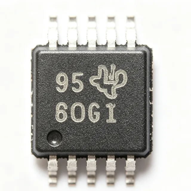
ADS1211U
ADS1211U - 24-Bit, 15.6 kSPS Delta-Sigma ADC | TI
The Texas Instruments ADS1211U is a 24-bit, 15.6 kSPS delta-sigma analog-to-digital converter with eight-channel input multiplexing, a programmable gain amplifier, an internal reference, and a 24-pin SOIC package. It operates from a single 5 V supply and is designed for precision conversion of differential, low-level analog signals. According to the Texas Instruments ADS1211 product page, the device provides 24-bit nominal resolution, 15.6 kSPS maximum data rate, programmable gain, and an integrated voltage reference.
A delta-sigma ADC is a type of analog-to-digital converter that uses continuous-time oversampling and digital filtering to provide high resolution and excellent noise performance. In the hierarchy of electronic components, the ADS1211U is a precision ADC, a data-conversion IC, and ultimately a semiconductor designed for measurement and instrumentation. Its low-noise architecture is useful when the input signal is small, slow, or generated by a sensitive transducer and does not require the very high sampling rates associated with SAR converters.
Key features include differential inputs, a programmable gain amplifier, a flexible SPI-compatible synchronous serial interface, and a two-wire control mode. The verified feature data also identifies programmable cutoff frequency and 23 effective bits at 10 Hz, with 20 effective bits at 1000 Hz. These characteristics allow the converter to balance conversion speed, filtering, and usable resolution according to the measurement bandwidth required by the application.
The ADS1211U uses a delta-sigma conversion architecture rather than a successive-approximation architecture. Digital filtering suppresses out-of-band noise, while the programmable cutoff frequency helps control bandwidth and the amount of averaging. The gain stage accepts low-level differential signals without requiring a separate instrumentation amplifier, although the complete signal chain still requires suitable source impedance, reference stability, and printed-circuit-board layout. The SPI-compatible interface supports conventional four-wire control, while two-wire mode can simplify isolated or pin-constrained systems.
Typical applications include low-level bridge and load-cell measurement, industrial process instrumentation, precision temperature sensing, laboratory data acquisition, battery monitoring, and compact sensor interfaces. Its 24-bit conversion word and differential inputs are particularly valuable when the measured quantity is represented by a small voltage difference. The single 5 V architecture can simplify system power design compared with converters requiring separate analog and digital rails.
Designers should verify the input voltage range, absolute maximum ratings, common-mode limits, PGA range, reference accuracy, and digital interface timing in the manufacturer datasheet before finalizing a circuit. Decoupling, grounding, and analog-versus-digital layout remain critical because they can affect the effective resolution otherwise provided by the converter. The available verified data does not include numeric timing values, pin assignments, or complete electrical limits, so those details should not be inferred from general ADC experience.
This page consolidates the verified Texas Instruments and distributor information, distinguishes documented parameters from unavailable data, and provides engineering-oriented application and design guidance beyond a basic catalog listing. It also records why only one web-supported same-package alternative is presented instead of padding the replacement list with unverified parts.
RFC
Hubungi kami