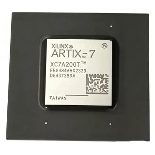
EP4CE15F23A7N - 15,408-LC Cyclone IV E FPGA | Altera
MPN: EP4CE15F23A7N ✓ AktifEP4CE15F23A7N Ringkasan
A field-programmable gate array is a programmable semiconductor belonging to the FPGA and CPLD hierarchy. Unlike a fixed-function application-specific integrated circuit, an FPGA contains configurable logic, memory, and programmable I/O structures that engineers can configure after manufacture. This makes Cyclone IV E devices useful for parallel processing, protocol bridging, control logic, signal acquisition, and embedded system adaptation.
The EP4CE15F23A7N combines 15,408 logic elements with 963 configurable logic blocks and operates at speeds up to 472.5 MHz. Its 484-ball FBGA package provides 343 I/O positions according to the distributor product listing, while the manufacturer identifies the F23 package configuration as a 23 mm by 23 mm, 1 mm-pitch device. This combination offers substantial routing and interface capacity for compact embedded platforms.
The Cyclone IV E architecture is intended for cost-sensitive, low-power programmable systems. Configuration data establishes the logic implemented by the FPGA, after which programmable I/O can connect to external memory, control signals, communications links, and mixed-signal peripherals. The 1.2 V supply figure in the device listing describes the core supply used by the FPGA architecture; board-level rails and I/O standards must be designed to satisfy the complete power architecture.
Typical uses include industrial control, test and measurement, communications infrastructure, embedded vision, and low-cost instrumentation. A design requiring deterministic parallel logic can map counters, finite-state machines, packet filters, or data pipelines into the 963 configurable logic blocks, while the 472.5 MHz maximum frequency provides ample timing margin for many control and interface functions when timing constraints are properly implemented.
The primary design consideration is package-level signal integrity. A 484-ball FBGA requires a multilayer PCB with short, impedance-controlled escape routes, solid power and ground planes, and careful decoupling around the device. Designers should use the manufacturer pin and package information for the exact F23 configuration and validate every power rail against the Cyclone IV E device requirements before releasing the layout.
This product record combines package-specific ordering information, verified device specifications, sourcing guidance, and practical design considerations. It also distinguishes genuine same-package alternatives from larger Cyclone IV E devices that are not drop-in replacements because their logic capacity differs materially.
Pilihan pengganti yang segera untuk EP4CE15F23A7N — sama paket, pin-pin kompatibel. Bahagian paket yang berbeza memerlukan kerja ulang PCB diasingkan.
Varietas dalam siri ini
Model serupa yang kompatibel dengan pengganti yang segera EP4CE15F23A7N (sama faktor bentuk dan kaki) — berbeza dalam Package, Speed Grade, Process Technology, Configuration Modes, Operating Temperature.
EP4CE15F23C7N
✅ Masuk Drop-InHubungi untuk harga
Lihat Datasheet →EP4CE15F23I7N
✅ Masuk Drop-InHubungi untuk harga
Lihat Datasheet →EP4CE15F23A8N
✅ Masuk Drop-In ⚠️ Spesifikasi Tidak Disahkan📋 Alternatif rujukan (tidak dalam katalog)
EP4CE15F23C8N
✅ Masuk Drop-In ⚠️ Spesifikasi Tidak DisahkanHubungi untuk harga
Lihat Datasheet →EP4CE15F23I8N
✅ Masuk Drop-In ⚠️ Spesifikasi Tidak Disahkan📋 Alternatif rujukan (tidak dalam katalog)
EP4CE15F23A7N Penilaian maksimum & Ciri-ciri Elektrik
| Device Type | Cyclone IV E field-programmable gate array |
| Logic Elements | 15,408 elements |
| Configurable Logic Blocks | 963 CLBs |
| Maximum Operating Frequency | 472.5 MHz |
| Core Supply Voltage | 1.2 V |
| Package Type | FBGA-484 |
| Package Code | F23 |
| Package Body Dimensions | 23 mm x 23 mm |
| Ball Pitch | 1.0 mm |
| I/O Count | 343 I/O |
| Embedded Memory | 516,096 bits |
| Gaya Pemasangan | Surface mount |
| Logic Blocks or Elements in Secondary Listing | 47 logic blocks |
| Primary Device Family | Cyclone IV E |
| Lead-Free Status | Lead free |
Panduan Konfigurasi Pin EP4CE15F23A7N 23 mm x 23 mm
Konfigurasi pin untuk EP4CE15F23A7N (23 mm x 23 mm pakai). IC digital ini termasuk GPIO, antaramuka komunikasi (UART, SPI, I2C), dan pin kuasa. Rujuk dokumen pengeluar untuk fungsi pin alternatif dan opsi konfigurasi. Biasa digunakan dalam rancangan sistem ter嵌入式 dan PCB.

Tiada data garisan pin yang diperoleh untuk EP4CE15F23A7N.
Rujuk kepada lembaran data untuk konfigurasi pin penuh.
Aplikasi Biasa
EP4CE15F23A7N patut untuk 6 aplikasis: Industrial Control and Automation, Test and Measurement Instrumentation, Communications Protocol Bridging, Embedded Vision and Image Preprocessing, Programmable Signal Conditioning, Low-Cost Embedded System Control.
Industrial Control and Automation
The EP4CE15F23A7N fits compact programmable controllers because its 15,408 logic elements and 963 configurable logic blocks can implement multiple state machines, interlocks, counters, and timing sequences in parallel. A 472.5 MHz maximum operating frequency also supports demanding control and bus logic while leaving timing margin for routed designs. Engineers can use the 343 I/O positions to connect sensors, actuators, encoders, and communication transceivers. The F23 484-ball FBGA should be placed on a multilayer PCB with short signal paths and robust power distribution. Before production use, confirm the exact grade, operating-temperature range, and lifecycle commitment against the industrial equipment specification.
Test and Measurement Instrumentation
In test and measurement equipment, programmable logic can implement acquisition control, trigger sequencing, digital calibration, and data-processing pipelines without relying on a fixed application-specific controller. The EP4CE15F23A7N provides 15,408 logic elements, 963 configurable logic blocks, and a maximum operating frequency of 472.5 MHz, making it suitable for parallel digital channels and moderately timed control paths. Its 516,096 bits of embedded memory can support buffering and data organization close to the programmable fabric. Board designers should isolate sensitive analog sections, use controlled clock distribution, and apply the manufacturer power and decoupling recommendations for the 1.2 V core architecture.
Communications Protocol Bridging
The EP4CE15F23A7N can implement protocol conversion, framing, filtering, and data-routing logic when multiple communication formats must be adapted within one embedded system. Its 963 configurable logic blocks provide substantial parallel capacity for finite-state machines and wide datapaths, while 343 I/O positions provide substantial board-level connectivity. At speeds up to 472.5 MHz, the device can support demanding serial, parallel, and packet-processing functions after appropriate clocking and timing closure. For high-speed links, preserve controlled-impedance routing, minimize stub effects, and use dedicated clock and data-path techniques. Configuration storage, clock jitter tolerance, and external transceiver requirements must also be validated.
Embedded Vision and Image Preprocessing
The Cyclone IV E architecture in the EP4CE15F23A7N can support embedded image pre-processing, pixel classification, threshold detection, and frame-format conversion where a programmable pipeline is preferable to a fixed controller. The 15,408 logic elements and 963 configurable logic blocks allow multiple parallel lanes to be assembled without introducing another processor solely for logic-intensive tasks. Its 472.5 MHz maximum frequency supports timed pipeline stages, while the 516,096-bit embedded-memory figure provides local data storage. Video designs should pay particular attention to clock recovery, pixel-clock alignment, I/O standards, and signal integrity between the image sensor, external memory interface, and FPGA.
Programmable Signal Conditioning
The EP4CE15F23A7N is suitable for programmable digital signal conditioning, including sampling-path control, digital filtering, pulse characterization, and interface adaptation. Its 963 configurable logic blocks can distribute processing across parallel channels, while the 15,408-element fabric offers a practical balance between logic capacity and routing complexity. A maximum operating frequency of 472.5 MHz permits timing-intensive implementations when the external clocking architecture and I/O standards are appropriate. For precision-sensitive systems, isolate the FPGA supply from analog sections, control clock jitter, use synchronous interfaces where possible, and verify timing with the actual external-device timing constraints.
Low-Cost Embedded System Control
The EP4CE15F23A7N can consolidate several fixed functions into a compact programmable controller for appliances, laboratory equipment, and specialized embedded products. A design may combine reset sequencing, watchdog logic, keypad scanning, display control, event logging, and communication routines within the 963 configurable logic blocks. The 1.2 V core supply and 484-ball FBGA package support integration on a multilayer PCB, although careful decoupling and ball-grid escape routing remain essential. Because the package has many balls and the architecture is performance-oriented, use conservative I/O timing, validate configuration startup, and confirm device grade and temperature requirements before committing to a high-volume design.
Data referensi kejuruteraan untuk EP4CE15F23A7N — perbandingan, panduan rancangan, dan maklumat kesediaan
Panduan Pilihan
Choose EP4CE15F23C7N or EP4CE15F23I7N only after confirming that their ordering suffix satisfies the required speed and temperature grade; both retain the same family and package, but a shared footprint does not prove identical operating characteristics. EP4CE15F23A8N, EP4CE15F23C8N, and EP4CE15F23I8N are alternatives to evaluate when a different grade or speed suffix is needed, provided the manufacturer ordering table confirms the exact requirements.
Avoid using EP4CE30F23C7N or EP4CE40F23C7N as drop-in substitutes. Their greater logic capacity changes routing, power, timing, and utilization assumptions, making them suitable for new designs that genuinely need more resources. Final qualification should include timing closure, temperature-grade review, lifecycle confirmation, and PCB validation using the exact F23 package documentation.
Perbandingan dengan Gantian
| Parametr | Produk Ini | EP4CE15F23C7N | EP4CE15F23I7N | EP4CE15F23A8N | EP4CE15F23C8N | EP4CE15F23I8N |
|---|---|---|---|---|---|---|
| Brand | Altera | Altera | Altera | Altera | Altera | Altera |
| Package | FBGA-484 (F23) | FBGA-484 (F23) | FBGA-484 (F23) | FBGA-484 (F23) | FBGA-484 (F23) | FBGA-484 (F23) |
| Device Family | Cyclone IV E | Cyclone IV E | Cyclone IV E | Cyclone IV E | Cyclone IV E | Cyclone IV E |
| Logic Elements | 15,408 elements | 15,408 elements | 15,408 elements | 15,408 elements | 15,408 elements | 15,408 elements |
| Configurable Logic Blocks | 963 CLBs | 963 CLBs | 963 CLBs | 963 CLBs | 963 CLBs | 963 CLBs |
| Core Supply Voltage | 1.2 V | 1.2 V | 1.2 V | 1.2 V | 1.2 V | 1.2 V |
| Package Dimensions | 23 mm x 23 mm | 23 mm x 23 mm | 23 mm x 23 mm | 23 mm x 23 mm | 23 mm x 23 mm | 23 mm x 23 mm |
| Ball Pitch | 1.0 mm | 1.0 mm | 1.0 mm | 1.0 mm | 1.0 mm | 1.0 mm |
| Grade Suffix | A7N | C7N | I7N | A8N | C8N | I8N |
Penyeberangsung Jelas
- Defined 15,408-element logic density (vsEP4CE30F23C7N)
- 472.5 MHz maximum operating frequency (vsEP4CE15F23C7N)
- Lower logic utilization than larger F23 devices (vsEP4CE40F23C7N)
- Compact 23 mm by 23 mm F23 package (vsEP4CE15F23I7N)
Catatan Desain
The EP4CE15F23A7N uses a 23 mm by 23 mm FBGA-484 package with a 1 mm ball pitch. Route power, ground, clock, and high-speed signals on a multilayer PCB with short escape paths, uninterrupted reference planes, and via arrangements that minimize loop area. Place decoupling capacitors close to the relevant supply balls and follow the manufacturer pin and layout guidance for the F23 package. A generic BGA footprint must not replace the package-specific land pattern.
Design the power tree around the 1.2 V core supply and every auxiliary rail identified in the F23 documentation. Check static and dynamic current at the chosen clock and I/O activity, then include regulator headroom for startup and configuration transients. Place bulk and local decoupling according to the manufacturer layout recommendations, and keep sensitive reference connections away from switching nodes and high-current return paths. Validate the rail sequence under worst-case configuration and I/O loading.
Use controlled-impedance routing for external clocks and high-speed interfaces, with matched reference planes and no unnecessary stubs. The 343 I/O positions provide considerable connectivity, but simultaneous switching can create power and ground disturbance. Analyze the selected I/O standards, termination, slew rate, and external load before assigning pins. If the design uses external memory, treat the memory interface as a complete timing and signal-integrity subsystem rather than treating the FPGA ball assignments as ordinary GPIO connections.
Do not select a same-looking Cyclone IV E ordering code without checking the resource tier and suffix meaning. EP4CE30F23C7N and EP4CE40F23C7N use the F23 package family but provide substantially more logic than EP4CE15F23A7N, so they are not parameter-matched drop-in substitutes. For EP4CE15F23 grade variants, verify the exact speed and temperature grade, confirm timing closure, and review configuration compatibility before approving a replacement.
Maklumat Kesediaan
The product listing identifies the EP4CE15F23A7N as lead free. Specific RoHS, REACH, AEC-Q100, halogen-free, and conflict-minerals declarations were not stated in the product text.