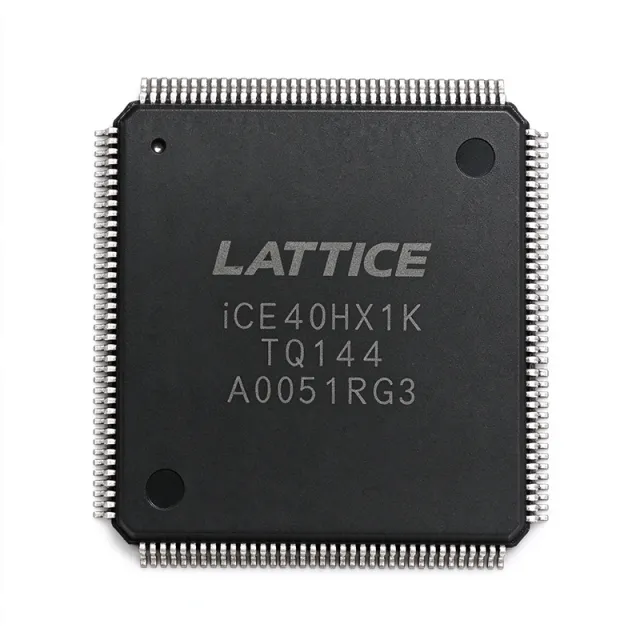
ICE40HX4K-TQ144 - 3520-LUT 1.2V FPGA | Lattice Semiconductor
MPN: ICE40HX4K-TQ144 ✓ Aktif| Kuantiti | Harga Satuan | Lengkap |
|---|---|---|
| 1 | $18.2813 | $18.28 |
| 10 | $13.2031 | $132.03 |
| 100 | $11.6797 | $1,167.97 |
| 500 | $11.1719 | $5,585.95 |
| 1,000 | $10.6641 | $10,664.10 |
ICE40HX4K-TQ144 Ringkasan
A field-programmable gate array is a configurable digital semiconductor that contains programmable logic blocks, routing resources, input/output blocks, and configuration memory. In the hierarchy, an FPGA is a programmable logic device, a digital IC, and a semiconductor. Unlike a fixed-function microcontroller or application-specific integrated circuit, an FPGA can be programmed after manufacture to implement parallel data paths, control logic, serial interfaces, and hardware signal processing.
The ICE40HX4K provides 3,520 logic cells and 81,920 bits of configuration memory, as identified by DigiKey and Mouser search results. Its 107 I/Os provide substantial connectivity for external memory, sensors, communications, control signals, and general-purpose digital interfaces. The HX family is positioned by Lattice as a low-power, high-performance FPGA family, making the part suitable for embedded control, communication, instrumentation, and education platforms where low static power and fast programmable logic are important.
The 144-pin TQFP package exposes the FPGA in a conventional surface-mount form factor suitable for automated assembly and multilayer PCB designs. The verified source snippets identify the package as 144-pin TQFP or 144-LQFP terminology; designers should confirm the exact mechanical drawing and pin names against the manufacturer datasheet before releasing a PCB footprint. The supplied data does not specify speed grade, temperature range, power consumption, pin names, memory architecture beyond configuration capacity, or I/O voltage limits.
Typical uses include custom interface controllers, low-power sensor aggregation, digital signal conditioning, communications adapters, test fixtures, and FPGA-based education or prototyping boards. For a new design, use the manufacturer’s configuration toolchain and verify pin assignments, supported I/O standards, clocking resources, power rails, decoupling requirements, and programming interface compatibility. Because the supplied evidence confirms the family and capacity but not a complete electrical characterization, unsupported values should not be inferred from generic iCE40 family claims.
Pilihan pengganti yang segera untuk ICE40HX4K-TQ144 — sama paket, pin-pin kompatibel. Bahagian paket yang berbeza memerlukan kerja ulang PCB diasingkan.
Varietas dalam siri ini
Model serupa yang kompatibel dengan pengganti yang segera ICE40HX4K-TQ144 (sama faktor bentuk dan kaki) — berbeza dalam Configuration Memory, Device Type, FPGA Family, Programmable Logic.
Alat Perbandingan Cepat — Pilih bahagian alternatif untuk perbandingan bersamaan:
ICE40HX4K-CB132
📋 Alternatif rujukan (tidak dalam katalog)
A3P060-TQG144I
📋 Alternatif rujukan (tidak dalam katalog)
ICE40HX4K-TQ144 Penilaian maksimum & Ciri-ciri Elektrik
| Device Type | Field-programmable gate array (FPGA) |
| FPGA Family | iCE40 HX |
| Logic Cells | 3,520 cells |
| Configuration Memory | 81,920 bits |
| Core Supply Voltage | 1.2 V |
| I/O Count | 107 I/Os |
| Kemasan | 144-pin TQFP |
| Process Technology | 40 nm |
| Programmable Logic | Field-programmable logic and routing |
| Power Class | Ultra-low-power FPGA |
| Application Class | Low-power digital logic design |
| Jenis Pemasangan | Surface mount |
Panduan Konfigurasi Pin ICE40HX4K-TQ144 144-pin tqfp
Konfigurasi pin untuk ICE40HX4K-TQ144 (144-pin tqfp pakai). IC digital ini termasuk GPIO, antaramuka komunikasi (UART, SPI, I2C), dan pin kuasa. Rujuk dokumen pengeluar untuk fungsi pin alternatif dan opsi konfigurasi. Biasa digunakan dalam rancangan sistem ter嵌入式 dan PCB.

Tiada data garisan pin yang diperoleh untuk ICE40HX4K-TQ144.
Rujuk kepada lembaran data untuk konfigurasi pin penuh.
Aplikasi Biasa
ICE40HX4K-TQ144 patut untuk 6 aplikasis: Custom Communications Interface, Low-Power Sensor Aggregation, Programmable Data Acquisition, FPGA Education and Prototyping, Instrument Control and Timing, Industrial Digital Control.
Custom Communications Interface
ICE40HX4K-TQ144 fits a custom communications interface when a design needs programmable parallel logic, clock-domain control, and flexible external connectivity. Its 3,520 logic cells provide implementation capacity for framing, packet filtering, buffering, and protocol conversion, while 107 I/Os support data buses, control signals, status indicators, and configuration or debug connections. The 1.2 V core supply aligns it with low-power programmable logic rather than a high-performance FPGA architecture. The engineer should use the Lattice toolchain to map clocking and I/O resources, then verify timing, voltage levels, and pin constraints in the manufacturer datasheet.
Disebarkan
Low-Power Sensor Aggregation
ICE40HX4K-TQ144 is suitable for consolidating multiple digital sensors into a compact control subsystem. Parallel sensor signals can be sampled, filtered, timestamped, and routed through programmable logic, while the 107 available I/Os provide connections to sensors, interrupt lines, and downstream processors. Its ultra-low-power family positioning is useful in embedded or battery-operated equipment, although actual current consumption depends on selected I/O, clocking, utilization, and voltage rails. Validate the sensor voltage levels, supported I/O standards, clock requirements, and power budget before committing to the part.
Disebarkan
Programmable Data Acquisition
ICE40HX4K-TQ144 can implement programmable acquisition logic for test, measurement, and industrial equipment. The FPGA structure allows parallel channels to be routed into custom pipelines, digital filters, state machines, or data-format converters without requiring a fixed application-specific IC. Its 3,520 logic cells and 107 I/Os provide a substantial design envelope for moderate channel counts. The main engineering trade-off is that the supplied data does not specify high-speed I/O performance, so the design must verify acquisition-rate targets and pin-level timing against the exact manufacturer documentation.
Disebarkan
FPGA Education and Prototyping
ICE40HX4K-TQ144 is well suited to FPGA education because it combines programmable logic with a conventional 144-pin surface-mount package and a stated capacity of 3,520 logic cells. Students can implement counters, state machines, UARTs, displays, memory interfaces, and hardware algorithms while learning configuration, timing, and pin assignment workflows. The part also supports projects that need more expansion than a very small FPGA without introducing a large BGA package. For production adoption, teams should still confirm package dimensions, toolchain compatibility, and open-source board availability.
Disebarkan
Instrument Control and Timing
ICE40HX4K-TQ144 can serve as a programmable timing and sequencing controller in instruments that coordinate triggers, relays, displays, counters, and external test fixtures. Its FPGA architecture enables parallel operations and deterministic control logic, while the 107-I/O package exposes enough pins for multiple instrument buses and status lines. The 1.2 V core supply is relevant to compact embedded systems, but power sequencing and I/O voltage compatibility must be designed explicitly. Validate all timing constraints and level-shift requirements using the manufacturer pin and electrical tables.
Disebarkan
Industrial Digital Control
ICE40HX4K-TQ144 is appropriate for industrial digital-control modules that combine logic sequencing, status monitoring, and external interface handling. Programmable logic can implement state machines, interlocks, pulse generation, data validation, and communication framing while the 107 I/Os connect to sensors, actuators, and human-interface circuitry. Its low-power FPGA positioning can help control system energy use, but industrial suitability requires verification of temperature limits, I/O tolerances, clock stability, and regulatory requirements that are not supplied here. A hardware prototype should test worst-case utilization and signal integrity.
Disebarkan
Ringkasan Produk Disebarkan
Data referensi kejuruteraan untuk ICE40HX4K-TQ144 — perbandingan, panduan rancangan, dan maklumat kesediaan
Panduan Pilihan
Perbandingan dengan Gantian
| Parametr | Produk Ini | ICE40HX4K-CB132 | A3P060-TQG144I |
|---|---|---|---|
| Package | 144-pin TQFP | CB132 | 144-pin TQFP |
| Brand | Lattice Semiconductor | Lattice Semiconductor | Actel |
| FPGA Family | iCE40 HX | iCE40 HX | Actel FPGA |
Penyeberangsung Jelas
- Higher verified I/O count than the cited A3P060 comparison part (vsA3P060-TQG144I)
- Same iCE40 HX family identity as the related Lattice option (vsICE40HX4K-CB132)
- Low-power FPGA positioning with a moderate 3,520-cell capacity (vsA3P060-TQG144I)
Catatan Desain
Use the exact Lattice Semiconductor mechanical drawing for the 144-pin TQFP footprint rather than relying on a generic TQFP library. Confirm package body size, lead pitch, pin numbering, solder-mask clearance, and assembly orientation before fabrication. The verified data confirms the package family and pin count but does not provide the mechanical dimensions.
Design the 1.2 V core rail and any required I/O rails from the manufacturer’s recommended power architecture. Place decoupling capacitors close to the supply and ground pins, and verify voltage tolerances, sequencing, current limits, and I/O levels against the exact datasheet. The supplied data does not specify regulator current or permissible rail combinations, so those values must not be guessed.
Plan the configuration path and boot behavior before assigning board-level pins. Confirm whether the design uses active configuration, another supported mode, and which pins are reserved by the FPGA. Also check the programming tool, file format, and any external flash requirement in the Lattice documentation; these details are not present in the supplied search snippets.
Keep clock inputs, sensitive interfaces, and high-speed programmable-logic routes away from noisy power-converter paths and provide a solid ground reference. Use the device timing report to evaluate setup and hold requirements, and validate I/O standards and drive strength only after confirming the pin-specific limits. The 107-I/O count is not itself evidence that every pin supports every voltage or protocol.
Maklumat Kesediaan
Compliance information was not included in the supplied verified web data. Confirm RoHS, REACH, automotive qualification, lead-free, halogen-free, and conflict-minerals status from the manufacturer or authorized distributor documentation.

