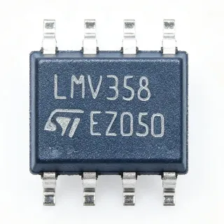
LM358FV-GE2 - Dual Op Amp, 8-SSOP | ROHM Semiconductor
MPN: LM358FV-GE2 ✓ AktifLM358FV-GE2 Ringkasan
An operational amplifier, or op amp, is a high-gain, differential-input amplifier used to amplify and buffer signals within electronic control systems. The dual-amplifier configuration belongs to the broader hierarchy of amplifier ICs, interface ICs, and analog semiconductors. Combining two amplifiers in one package reduces board area and simplifies designs requiring matched gain stages, active filters, sensor amplification, or feedback-control loops.
The LM358FV-GE2 combines a maximum offset voltage of 3 mV at 25°C with typical quiescent current of 0.35 mA per channel. Its 0.7 MHz gain-bandwidth product supports moderate-bandwidth signal conditioning, while its 0.3 V/µs slew rate determines large-signal response. The 3 V to 32 V operating supply range accommodates both conventional 5 V analog systems and higher industrial supply rails.
The ROHM LM358 device uses an internal arrangement intended for general-purpose precision and control rather than high-speed signal processing. Operation from a single positive supply or a split-supply configuration supports both single-ended and ground-centered signal systems. Designers should account for input common-mode limits, output swing, stability, and power-supply headroom according to the manufacturer application guidance.
Typical uses include industrial sensor interfaces, transducer conditioning, active filters, loop-control amplifiers, low-frequency data-acquisition channels, and general buffer stages. Its dual-channel arrangement is particularly useful when a board needs two similar amplifier functions without allocating two separate packages and their associated routing and decoupling requirements.
Place input, output, and supply bypass capacitors close to the relevant pins, and route high-current return paths to minimize ground offsets. Verify that signal amplitudes remain within the input and output common-mode limits across the complete supply range and temperature range. Adequate supply decoupling and careful stability analysis are essential in feedback configurations.
This product record combines the confirmed electrical and package characteristics with practical application guidance, comparison data, and design checks. Use the ROHM Semiconductor datasheet and pin-description table for final schematic, footprint, and operating-limit verification before placing a production order.
Pilihan pengganti yang segera untuk LM358FV-GE2 — sama paket, pin-pin kompatibel. Bahagian paket yang berbeza memerlukan kerja ulang PCB diasingkan.
Tiada pilihan pengganti yang segera untuk produk ini.
Minta AlternatifLM358FV-GE2 Penilaian maksimum & Ciri-ciri Elektrik
| Number of Channels | 2 circuits |
| Total Supply Voltage, Minimum | 3 V |
| Total Supply Voltage, Maximum | 32 V |
| Gain-Bandwidth Product, Typical | 0.7 MHz |
| Slew Rate, Typical | 0.3 V/µs |
| Input Offset Voltage, Maximum at 25°C | 3 mV |
| Quiescent Current per Channel, Typical | 0.35 mA |
| Amplifier Type | General-purpose operational amplifier |
| Kemasan | 8-SSOPB |
| Jenis Pemasangan | Surface mount |
| RoHS Classification | RoHS3 compliant |
| Export Control Classification | EAR99 |
Panduan Konfigurasi Pin LM358FV-GE2 8-ssopb
Konfigurasi pin untuk LM358FV-GE2 (8-ssopb pakai). Komponen analog ini mempunyai pin masukan, keluaran, dan kuasa. Rujuk dokumen pengeluar untuk konfigurasi pengecualian, pemulihan, dan pin aktifkan. Ideal untuk pengawasan isyarat dan litar pengukur.

Tiada data garisan pin yang diperoleh untuk LM358FV-GE2.
Rujuk kepada lembaran data untuk konfigurasi pin penuh.
Aplikasi Biasa
LM358FV-GE2 patut untuk 6 aplikasis: Industrial Sensor Signal Conditioning, Active Audio Filtering, Process Control Loop Amplification, Data Acquisition Front End, Voltage Reference Buffering, Battery-Powered Monitoring Circuit.
Industrial Sensor Signal Conditioning
The LM358FV-GE2 is appropriate for amplifying and buffering low-bandwidth transducer signals in industrial measurement systems. Its two channels can support related gain or filtering functions without requiring separate packages, while the 3 V to 32 V supply range accommodates 5 V electronics and higher industrial rails. The 0.7 MHz typical gain-bandwidth product and 0.3 V/µs slew rate suit slow sensor signals rather than wideband acquisition. Check the input common-mode range, maximum input bias current, output swing, and noise requirements against the manufacturer datasheet before fixing the gain network.
Disebarkan
Active Audio Filtering
The LM358FV-GE2 can implement first-order active filters and low-frequency audio signal-conditioning networks when wideband performance is unnecessary. Its dual-channel construction allows a filter and buffer to share one 8-SSOPB package, reducing component count and PCB area. The 0.7 MHz typical gain-bandwidth product is comfortably above many audio-frequency filter requirements, while the 0.3 V/µs slew rate constrains large-amplitude response. Confirm output swing, noise, stability with the selected feedback network, and power-supply decoupling before using the device in a precision audio path.
Disebarkan
Process Control Loop Amplification
The LM358FV-GE2 can serve as an error amplifier or controller-output driver in slow feedback loops used for heaters, valves, and other process-control systems. A 3 V to 32 V total supply range provides flexibility between low-voltage logic-side circuitry and industrial control rails, while the two channels support complementary or cascaded control functions. The device’s 0.7 MHz typical bandwidth and 0.3 V/µs slew rate suit loops well below high-speed communication rates. Verify output-current capability, load stability, saturation recovery, and thermal behavior under the worst actuator-drive condition.
Disebarkan
Data Acquisition Front End
The LM358FV-GE2 is useful in low-speed data-acquisition circuits where sensor or divider outputs require buffering before an ADC input. Its 3 mV maximum input offset voltage at 25°C provides a documented starting point for error budgeting, while two channels allow simultaneous signal conditioning or differential-to-single-ended stages where the circuit topology permits. The 0.7 MHz gain-bandwidth product limits the useful bandwidth well below high-speed ADC requirements. Check settling behavior, input bias current, common-mode limits, and ADC drive impedance in the complete signal chain.
Disebarkan
Voltage Reference Buffering
The LM358FV-GE2 can buffer a reference voltage when the circuit requires more drive capability than a passive reference node can provide. The dual-channel arrangement permits one channel to buffer the reference while the other handles an associated scaling or gain function. Its 3 V to 32 V supply range supports varied analog rails, and the 0.7 MHz typical gain-bandwidth product is sufficient for many reference buffers. The 3 mV maximum input offset at 25°C should be included in the error budget, and output-accuracy drift, load current, noise, and stability must be checked for the chosen reference.
Disebarkan
Battery-Powered Monitoring Circuit
The LM358FV-GE2 can support low-power monitoring, threshold, and current-buffer functions in battery-operated equipment. Its typical quiescent current of 0.35 mA per channel provides a useful starting point for power-budget analysis, and the 3 V minimum supply permits operation from a single 3.3 V or 5 V rail. Two channels can implement threshold detection and signal conditioning in one 8-SSOPB package. Actual battery life depends on total supply current, duty cycle, load, and regulator efficiency, so validate the complete operating profile and confirm output behavior during battery discharge.
Disebarkan
Ringkasan Produk Disebarkan
Data referensi kejuruteraan untuk LM358FV-GE2 — perbandingan, panduan rancangan, dan maklumat kesediaan
Panduan Pilihan
Perbandingan dengan Gantian
| Parametr | Produk Ini |
|---|---|
| Brand | ROHM Semiconductor |
| Package | 8-SSOPB |
| Number of Channels | 2 circuits |
| Total Supply Voltage Range | 3 V to 32 V |
| Gain-Bandwidth Product, Typical | 0.7 MHz |
| Slew Rate, Typical | 0.3 V/µs |
| Input Offset Voltage, Maximum at 25°C | 3 mV |
| Quiescent Current per Channel, Typical | 0.35 mA |
| RoHS Classification | RoHS3 compliant |
| Export Control Classification | EAR99 |
Penyeberangsung Jelas
- Two amplifiers in one compact package (vsLM358ADR)
- Wide total supply-voltage range (vsLM358ADR)
- Defined low-power operating characteristics (vsLM358ADR)
Catatan Desain
Do not treat every LM358-family ordering code as a drop-in substitute. LM358FV-GE2 is specified in an 8-SSOPB package, and package suffixes can indicate different lead styles, temperature grades, packing methods, or qualification levels. Confirm the land pattern, numbered pin assignments, electrical ratings, and traceback requirements before approving an alternative.
Place the supply bypass capacitor close to the amplifier supply pins and connect the exposed or ground-return path to a low-impedance plane. Keep input and feedback traces short, avoid routing them beneath noisy power paths, and maintain symmetric feedback loops where practical. Use a solid ground reference beneath the package when the PCB design and thermal requirements permit.
Validate every feedback network for stability with the output load and parasitic capacitance present on the assembled board. The 0.7 MHz typical gain-bandwidth product makes the LM358FV-GE2 suitable for many low-frequency tasks, but high closed-loop gain, capacitive loading, or excessive loop gain can affect settling and oscillation. Add an isolation resistor at capacitive loads only after checking its effect on gain and offset.
Estimate worst-case power dissipation from the actual total supply voltage, output voltage, quiescent current, and load current. The confirmed 0.35 mA typical quiescent current per channel is only the internal baseline and does not include output load current. Confirm operating-temperature limits, copper thermal performance, and adjacent heat sources before using the 8-SSOPB package in a high-load design.
Maklumat Kesediaan
The LM358FV-GE2 comparison record identifies RoHS3 compliance and EAR99 export classification. Compliance attributes not stated for this exact MPN remain unknown.