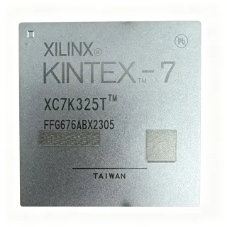
XCKU040-3FBVA676E - Kintex UltraScale FPGA | AMD
MPN: XCKU040-3FBVA676E ✓ AktifXCKU040-3FBVA676E Ringkasan
A field-programmable gate array is a semiconductor whose digital logic blocks, routing, block RAM, and programmable I/O can be configured after manufacture. The Kintex UltraScale family extends this programmable-device concept into ASIC-like parallel processing systems. Within the FPGA hierarchy, the XCKU040 belongs to the Kintex UltraScale product line, combines FPGA fabric with dedicated high-speed serial resources, and is positioned between lower-density programmable logic and the largest ASIC-class devices.
Key characteristics of the XCKU040-3FBVA676E include 312 I/O, a 676-ball FCBGA package, and the -3 performance grade. The large ball count supports a substantial interface complement, while the Kintex UltraScale architecture is suited to high-throughput datapaths requiring wide parallel transfers. The package uses ball-grid technology rather than perimeter leads, supporting dense routing of power, ground, configuration, and user signals across the device. Detailed logic-cell, memory, and high-speed transceiver counts should be taken from the current AMD Kintex UltraScale data sheet and product-selection tables for the exact device variant.
The -3 suffix denotes the highest performance grade offered for XCKU040 devices, making this ordering option appropriate when timing closure must be achieved at demanding clock rates. Designers should distinguish device speed grade, package suffix, and operating-temperature designation when comparing orderable parts: changing the speed grade changes timing characteristics, while changing the package changes the PCB land pattern and may also change the power-management design.
Typical deployments include high-throughput data processing, network packet handling, high-performance computing accelerators, video and image pipelines, telecommunications infrastructure, and industrial systems that consolidate multiple fixed-function blocks into one programmable device. The 312 I/O sites are useful for parallel control planes, external memory interfaces, and general-purpose peripheral connections, while dedicated UltraScale resources support high-speed serial links.
PCB design requires careful attention to the 676-ball FCBGA footprint, multilayer board construction, power-plane integrity, and via access beneath the device. Use the AMD package pinout files and board-design guidance to assign every ball, and validate high-speed interfaces with the vendor-recommended constraints. Because the ball grid hides most connections under the package, PCB inspection and test-point planning are especially important after assembly.
This page organizes the verified package, interface, and family information into an engineering-focused reference and separates device-selection facts from application guidance. It also identifies same-package XCKU040 ordering options for migration planning while directing designers to AMD documentation for authoritative ball assignments, timing limits, and power budgets.
Pilihan pengganti yang segera untuk XCKU040-3FBVA676E — sama paket, pin-pin kompatibel. Bahagian paket yang berbeza memerlukan kerja ulang PCB diasingkan.
XCKU040-2FBVA676E
✅ Masuk Drop-In ⚠️ Spesifikasi Tidak DisahkanHubungi untuk harga
Lihat Datasheet →XCKU040-1FBVA676E
✅ Masuk Drop-In ⚠️ Spesifikasi Tidak Disahkan📋 Alternatif rujukan (tidak dalam katalog)
XCKU040-3FBVA676I
✅ Masuk Drop-In ⚠️ Spesifikasi Tidak Disahkan📋 Alternatif rujukan (tidak dalam katalog)
XCKU040-2FBVA676I
✅ Masuk Drop-In ⚠️ Spesifikasi Tidak DisahkanHubungi untuk harga
Lihat Datasheet →XCKU040-1FBVA676I
✅ Masuk Drop-In📋 Alternatif rujukan (tidak dalam katalog)
XCKU040-3FBVA676E Penilaian maksimum & Ciri-ciri Elektrik
| Device Type | Kintex UltraScale field-programmable gate array (FPGA) |
| Programmable Architecture | All Programmable Architecture |
| User I/O Count | 312 I/O |
| Performance Grade | -3 speed grade |
| Speed Grade Positioning | -3 is the highest-performance XCKU040 speed grade |
| Package Type | 676-BBGA, FCBGA |
| Package Ball Count | 676 balls |
| Package Shape | Square ball-grid array |
| Terminal Form | Ball |
| Jenis Pemasangan | Surface mount |
Panduan Konfigurasi Pin XCKU040-3FBVA676E square ball-grid array
Konfigurasi pin untuk XCKU040-3FBVA676E (square ball-grid array pakai). IC digital ini termasuk GPIO, antaramuka komunikasi (UART, SPI, I2C), dan pin kuasa. Rujuk dokumen pengeluar untuk fungsi pin alternatif dan opsi konfigurasi. Biasa digunakan dalam rancangan sistem ter嵌入式 dan PCB.

Tiada data garisan pin yang diperoleh untuk XCKU040-3FBVA676E.
Rujuk kepada lembaran data untuk konfigurasi pin penuh.
Aplikasi Biasa
XCKU040-3FBVA676E patut untuk 6 aplikasis: High-Performance Network Packet Processing, Video and Image Processing Pipelines, High-Performance Computing Accelerators, Telecommunications Infrastructure Equipment, Industrial Control and Automation Systems, Aerospace and Defense Data Processing.
High-Performance Network Packet Processing
The XCKU040-3FBVA676E fits packet-processing systems that require wide parallel classification, buffering, and forwarding datapaths. Its 312 user I/O sites support parallel interfaces to external packet-buffer memory, control processors, and network management components, while the -3 grade supplies additional timing margin over lower XCKU040 speed grades. The design can place protocol parsing, lookup, queue management, and traffic shaping into programmable logic instead of a collection of fixed-function ASICs. Practical implementation still depends on memory bandwidth, packet timing, and board-level I/O timing. Use AMD UltraScale constraints and the official package pinout files when assigning balls and constraining interfaces.
Disebarkan
Video and Image Processing Pipelines
The XCKU040-3FBVA676E is suitable for parallel video, imaging, and sensor-processing pipelines where pixel throughput and deterministic latency are central requirements. The 312-I/O interface can support multiple parallel data buses and control channels, allowing capture, color conversion, filtering, and pre-processing stages to be consolidated in one FPGA. The -3 speed grade is useful when timing closure cannot be achieved comfortably in a lower speed grade. Board-level signal integrity remains a separate concern: high-resolution interfaces should use controlled-impedance routing, source-synchronous clocking, and vendor-recommended I/O standards. Validate the chosen pixel rate against the selected I/O standard and external memory timing.
Disebarkan
High-Performance Computing Accelerators
The XCKU040-3FBVA676E can serve as a programmable accelerator for DSP, linear-algebra, or specialized datapath functions that benefit from dense parallel logic. Its -3 performance grade provides additional timing margin when pipelines operate at aggressive clock rates, and the large package exposes 312 user I/O for high-bandwidth host, memory, or accelerator-board communication. Designers can implement custom fixed-point, floating-point, or control pipelines and scale them across the fabric rather than relying on a general-purpose processor. The main trade-offs are tool-chain effort, board complexity, and thermal management. Use AMD synthesis and implementation results to evaluate achievable timing, and validate power against the actual utilization profile rather than a nominal device figure.
Disebarkan
Telecommunications Infrastructure Equipment
The XCKU040-3FBVA676E is appropriate for telecommunications infrastructure that combines high-speed serial links with parallel packet-processing logic. Kintex UltraScale devices integrate dedicated high-speed resources with programmable fabric, allowing one device to implement transport functions, framing, aggregation, monitoring, and control-plane logic. The 676-ball FCBGA supports dense power and signal distribution required by such equipment. Exact transceiver counts and line rates depend on the selected XCKU040 configuration and must be confirmed in the AMD data sheet. PCB implementation should preserve the reference clock path, isolate sensitive rails as directed, and follow AMD power, decoupling, and high-speed layout guidance to prevent signal degradation.
Disebarkan
Industrial Control and Automation Systems
The XCKU040-3FBVA676E can consolidate machine-control logic, motion sequencing, diagnostics, and communication gateways in one programmable device. Its 312 user I/O sites provide substantial connectivity for sensors, actuators, fieldbus gateways, and safety-monitoring logic, while programmable hardware supports deterministic timing independent of a hosted processor. The -3 grade helps close demanding control loops, although thermal performance and long-term supply conditions must be evaluated for the deployment environment. Keep noisy power and high-speed communication sections separated in the PCB stack-up, use tested transceiver isolation techniques, and verify all timing paths against the selected operating speed and temperature grade.
Disebarkan
Aerospace and Defense Data Processing
The XCKU040-3FBVA676E can support programmable data-processing, telemetry, radar, and electronic-support functions where design flexibility and deterministic logic are valuable. The large 676-ball FCBGA provides extensive pin access, and the -3 grade offers timing margin for parallel algorithms. Qualification depends on the exact ordering suffix, screening process, operating-temperature range, and program requirements, so the device grade must be confirmed against the AMD product table rather than inferred from the family name. Design teams should also evaluate radiation effects, reliability monitoring, controlled-material requirements, and package-level thermal conditions as separate qualification activities.
Disebarkan
Ringkasan Produk Disebarkan
Data referensi kejuruteraan untuk XCKU040-3FBVA676E — perbandingan, panduan rancangan, dan maklumat kesediaan
Panduan Pilihan
Perbandingan dengan Gantian
| Parametr | Produk Ini | XCKU040-2FBVA676E | XCKU040-1FBVA676E | XCKU040-3FBVA676I | XCKU040-2FBVA676I | XCKU040-1FBVA676I |
|---|---|---|---|---|---|---|
| Brand | AMD | AMD | AMD | AMD | AMD | AMD |
| Package | 676-BBGA, FCBGA | 676-BBGA, FCBGA - same | 676-BBGA, FCBGA - same | 676-BBGA, FCBGA - same | 676-BBGA, FCBGA - same | 676-BBGA, FCBGA - same |
| Device Family | Kintex UltraScale FPGA | Kintex UltraScale FPGA | Kintex UltraScale FPGA | Kintex UltraScale FPGA | Kintex UltraScale FPGA | Kintex UltraScale FPGA |
| User I/O Count | 312 I/O | 312 I/O | 312 I/O | 312 I/O | 312 I/O | 312 I/O |
| Performance Grade | -3, highest-performance XCKU040 grade | -2 | -1 | -3 | -2 | -1 |
| Temperature Suffix | Commercial-temperature E suffix | E | E | I, industrial-temperature grade | I, industrial-temperature grade | I, industrial-temperature grade |
| Programming File Compatibility | XCKU040 device architecture; bitstream details require verification | Same XCKU040 architecture; speed-grade constraints still apply | Same XCKU040 architecture; speed-grade constraints still apply | Same XCKU040 architecture; temperature-grade constraints still apply | Same XCKU040 architecture; speed-grade constraints still apply | Same XCKU040 architecture; speed-grade constraints still apply |
Penyeberangsung Jelas
- Highest-performance speed grade in the XCKU040 family (vsXCKU040-2FBVA676E)
- Same speed grade with an alternate temperature designation (vsXCKU040-1FBVA676I)
- Performance migration without changing the PCB footprint (vsXCKU040-1FBVA676E)
- Industrial-temperature family alternative in the same land pattern (vsXCKU040-2FBVA676I)
Catatan Desain
Use the AMD UltraScale package pinout files to create the 676-ball land pattern and PCB constraints. Because the FCBGA conceals most connections, provide via access under the device where the AMD board-design guidance permits it, and avoid placing test pads or split-plane transitions that interfere with power-distribution continuity. Validate escape-routing length, reference-clock isolation, and high-speed pair symmetry before fabrication.
Estimated power must be calculated from the AMD XCKU040 power tables using the selected VCCINT, VCCAUX, and VCCO rails, clock rates, and design utilization. Multiply rail power by the regulator efficiency and add local distribution loss, then size the design for the highest expected ambient temperature. Do not reuse a nominal device figure because unused FPGA fabric may be biased up or down to reduce static power.
A shared 676-ball footprint does not make every XCKU040 ordering code electrically interchangeable. Confirm the speed grade, temperature grade, voltage configuration, and package drawing before substituting an alternative. After any speed-grade migration, rerun synthesis, implementation, static timing analysis, and board-level interface validation; a mechanical fit alone does not preserve timing closure.
The XCKU040-3FBVA676E is a high-performance, high-pin-count package whose actual dissipation depends strongly on design activity. Use the device-specific thermal model and the implemented design report rather than an unqualified power figure. Preserve copper area beneath the package, evaluate the PCB stack-up and airflow path, and check junction-temperature margin at the worst operating corner.
Maklumat Kesediaan
The family data confirms the XCKU040 device and package identifiers but does not provide explicit RoHS, REACH, lead-free, halogen-free, or conflict-minerals declarations for this exact ordering code. Verify the current regulatory documentation for the exact suffix and assembly site.