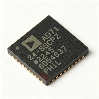
AD1674TD/883B - 12-Bit 100kSPS ADC | Analog Devices | Military
MPN: AD1674TD/883B ✓ Active| Qty | Unit Price | Extended |
|---|---|---|
| 1 | $89.5 | $89.50 |
| 10 | $82 | $820.00 |
| 100 | $74 | $7,400.00 |
| 500 | $66 | $33,000.00 |
| 1,000 | $58 | $58,000.00 |
AD1674TD/883B Overview
An analog-to-digital converter (ADC) is an electronic component that converts a continuous analog voltage into a discrete digital representation. The AD1674 is a successive-approximation register (SAR) ADC, which uses a binary search algorithm to determine the digital output. SAR ADCs are known for their high speed, low power, and ease of use, making them suitable for a wide range of applications from industrial control to data acquisition. The AD1674 belongs to the family of 12-bit ADCs, which provide 4096 discrete levels, offering a good balance between resolution and cost.
Key features of the AD1674TD/883B include a 12-bit resolution with a maximum sampling rate of 100 kSPS, a parallel output interface compatible with 8- and 16-bit microprocessors, and both AC and DC specifications that are fully tested. The device is packaged in a 28-pin ceramic dual-in-line package (CDIP) with side-brazed leads, ensuring robust mechanical and thermal performance. The military-grade temperature range of -55°C to +125°C and compliance with MIL-STD-883 screening make it suitable for extreme environments.
The AD1674 is implemented using Analog Devices' BiMOS II process, which combines high-performance bipolar analog circuitry with low-power CMOS digital logic on a single die. This architecture enables the integration of the SHA, reference, and clock without external components, simplifying system design. The device features a 10V internal reference with a typical temperature drift of 10 ppm/°C, ensuring stable operation over temperature. The three-state output buffers allow the ADC to share a data bus with other peripherals, reducing system complexity.
Typical applications for the AD1674TD/883B include military avionics, radar signal processing, industrial process control, and precision data acquisition systems. Its high accuracy and wide input range make it ideal for applications requiring reliable conversion in harsh conditions. The device is pin-compatible with the industry-standard AD574A and AD674A, allowing easy upgrades in existing designs.
When designing with the AD1674TD/883B, ensure that the analog input is properly buffered and that the reference is decoupled with a 10µF tantalum capacitor to minimize noise. The digital supply should be separated from the analog supply to avoid coupling digital switching noise into the analog path. The conversion start (RC) pin should be triggered with a clean pulse to avoid metastability issues.
Drop-in alternatives for AD1674TD/883B — same package, pin-to-pin compatible. Different-package parts requiring PCB rework are excluded.
Quick Comparison Tool — Select alternative parts for side-by-side comparison:
AD1674TD
✅ Drop-In📋 Reference alternative (not in catalog)
AD1674JNZ
✅ Drop-In📋 Reference alternative (not in catalog)
AD1674KNZ
✅ Drop-In📋 Reference alternative (not in catalog)
AD574AJD
✅ Drop-In ⚠️ Specs Unverified📋 Reference alternative (not in catalog)
AD674AJD
✅ Drop-In ⚠️ Specs Unverified📋 Reference alternative (not in catalog)
ADS7816
✅ Drop-In ⚠️ Specs Unverified📋 Reference alternative (not in catalog)
AD1674TD/883B Maximum Ratings & Electrical Characteristics
| Resolution | 12 bits |
| Sampling Rate | 100 kSPS |
| Number of Inputs | 1 |
| Input Type | Single Ended |
| Input Ranges | 0V to 10V, 0V to 20V, ±5V, ±10V |
| Interface | Parallel |
| Architecture | SAR |
| Reference Type | Internal, 10V |
| Supply Voltage | +5V (logic), ±12V or ±15V (analog) |
| Operating Temperature | -55°C to +125°C |
| Package | 28-CDIP (Side Brazed) |
| Mounting Type | Through Hole |
| Screening Level | Military (MIL-STD-883) |
| RoHS Status | Non-compliant (military grade) |
| Pin Compatibility | AD574A, AD674A |
AD1674TD/883B Pin Configuration
| Pin 1 | VLOGIC — Logic supply voltage (+5V) |
| Pin 2 | 12/8 — Data format select (12-bit or 8-bit) |
| Pin 3 | CS — Chip select (active low) |
| Pin 4 | A0 — Address input for byte selection |
| Pin 5 | R/C — Read/convert select |
| Pin 6 | CE — Chip enable (active high) |
| Pin 7 | VCC — Analog positive supply (+12V or +15V) |
| Pin 8 | REF OUT — Reference output (10V) |
| Pin 9 | AGND — Analog ground |
| Pin 10 | REF IN — Reference input |
| Pin 11 | VEE — Analog negative supply (-12V or -15V) |
| Pin 12 | BIP OFF — Bipolar offset |
| Pin 13 | 10V IN — 10V range input |
| Pin 14 | 20V IN — 20V range input |
| Pin 15 | DGND — Digital ground |
| Pin 16 | DB11 (MSB) — Data bit 11 (most significant) |
| Pin 17 | DB10 — Data bit 10 |
| Pin 18 | DB9 — Data bit 9 |
| Pin 19 | DB8 — Data bit 8 |
| Pin 20 | DB7 — Data bit 7 |
| Pin 21 | DB6 — Data bit 6 |
| Pin 22 | DB5 — Data bit 5 |
| Pin 23 | DB4 — Data bit 4 |
| Pin 24 | DB3 — Data bit 3 |
| Pin 25 | DB2 — Data bit 2 |
| Pin 26 | DB1 — Data bit 1 |
| Pin 27 | DB0 (LSB) — Data bit 0 (least significant) |
| Pin 28 | STS — Status output (busy) |
Typical Applications
AD1674TD/883B is suitable for 6 applications: Military Avionics, Industrial Process Control, Data Acquisition Systems, Test and Measurement Equipment, Medical Imaging, Aerospace Telemetry.
Military Avionics
The AD1674TD/883B is ideal for military avionics systems that require high-reliability analog-to-digital conversion in extreme environments. Its military temperature range (-55°C to +125°C) and MIL-STD-883 screening ensure dependable operation in aircraft and missile systems. The 12-bit resolution and 100 kSPS sampling rate are sufficient for flight control, navigation, and engine monitoring. The internal reference and sample-and-hold amplifier reduce external component count, saving space in avionics racks. The parallel interface simplifies connection to mission computers and data buses.
Recommended
Industrial Process Control
In industrial process control, the AD1674TD/883B provides accurate conversion of sensor signals such as temperature, pressure, and flow. Its multiple input ranges (0-10V, 0-20V, ±5V, ±10V) allow direct connection to various transducers without external scaling. The 12-bit resolution offers 0.024% of full-scale accuracy, suitable for precise control loops. The device's robust ceramic package and wide temperature range make it reliable in factory environments. The parallel output can interface with PLCs and microcontrollers, enabling real-time monitoring and control.
Recommended
Data Acquisition Systems
The AD1674TD/883B is a core component in data acquisition systems, converting analog signals from sensors and transducers into digital data for processing and storage. Its 100 kSPS sampling rate allows capturing dynamic signals with adequate fidelity. The internal sample-and-hold amplifier ensures accurate conversion of fast-changing inputs. The three-state output buffers enable multiple ADCs to share a common data bus, simplifying system design. The device's low power consumption and single +5V logic supply make it suitable for portable and remote data loggers.
Recommended
Test and Measurement Equipment
The AD1674TD/883B is used in test and measurement equipment such as digital multimeters, oscilloscopes, and spectrum analyzers. Its high accuracy and low noise performance ensure precise measurements. The wide input range accommodates various signal levels, from millivolt sensor outputs to high-voltage signals. The parallel interface allows fast data transfer to display and processing units. The military-grade reliability is beneficial for field-testing equipment used in harsh conditions. The device's internal reference reduces calibration requirements, simplifying instrument design.
Recommended
Medical Imaging
In medical imaging systems, the AD1674TD/883B converts analog signals from sensors such as photodiodes and ultrasound transducers into digital data for image reconstruction. Its 12-bit resolution provides sufficient dynamic range for diagnostic imaging. The 100 kSPS sampling rate is adequate for many imaging modalities. The device's low noise and high linearity ensure accurate representation of tissue structures. The military-grade temperature range is not typically required, but the device's reliability is beneficial in critical medical equipment. The parallel interface allows high-speed data transfer to image processors.
Recommended
Aerospace Telemetry
The AD1674TD/883B is used in aerospace telemetry systems to convert sensor data from spacecraft and launch vehicles into digital format for transmission to ground stations. Its high reliability and wide temperature range are essential for space applications. The 12-bit resolution and 100 kSPS sampling rate are suitable for monitoring various parameters such as temperature, pressure, and vibration. The device's radiation tolerance, while not explicitly specified, is enhanced by the ceramic package and military screening. The parallel interface allows integration with telemetry encoders and transmitters.
Recommended
Recommended Products Summary
Engineering reference data for AD1674TD/883B — comparison, design guidance, and compliance information.
Selection Guide
Comparison with Alternatives
| Parameter | This Product | AD1674TD | AD1674JNZ | AD574AJD | ADS7816 |
|---|---|---|---|---|---|
| Package | 28-CDIP | 28-CDIP | 28-PDIP | 28-CDIP | 28-CDIP |
| Brand | Analog Devices | Analog Devices | Analog Devices | Analog Devices | Texas Instruments |
| Resolution | 12 bits | 12 bits | 12 bits | 12 bits | 12 bits |
| Sampling Rate | 100 kSPS | 100 kSPS | 100 kSPS | 35 kSPS | 200 kSPS |
| Temperature Range | -55°C to +125°C | -55°C to +125°C | 0°C to +70°C | -55°C to +125°C | -40°C to +85°C |
| Input Ranges | 0-10V, 0-20V, ±5V, ±10V | 0-10V, 0-20V, ±5V, ±10V | 0-10V, 0-20V, ±5V, ±10V | 0-10V, 0-20V, ±5V, ±10V | 0-5V (differential) |
| Interface | Parallel | Parallel | Parallel | Parallel | Serial |
| Internal Reference | Yes (10V) | Yes (10V) | Yes (10V) | Yes (10V) | Yes (2.5V) |
Key Differentiators
- Military-grade screening (MIL-STD-883) (vs AD1674JNZ)
- Wider temperature range (vs AD1674JNZ)
- Higher sampling rate than AD574A (vs AD574AJD)
Design Notes
The AD1674TD/883B requires multiple supply rails: +5V for logic, and ±12V or ±15V for the analog circuitry. Ensure that the analog supplies are well-regulated and decoupled with 10µF tantalum capacitors in parallel with 0.1µF ceramic capacitors close to the VCC and VEE pins. The logic supply should be isolated from the analog supplies to prevent digital noise from coupling into the analog path. A ground plane is recommended to minimize noise.
For optimal performance, place the AD1674TD/883B on a PCB with a solid ground plane. Separate analog and digital ground areas and connect them at a single point, typically near the DGND pin. Keep analog input traces short and shielded from digital signals. The reference output (REF OUT) should be bypassed with a 10µF tantalum capacitor to ground to stabilize the internal reference. Ensure that the digital output traces are not routed parallel to analog input traces to avoid crosstalk.
A common mistake is driving the analog input beyond the specified ranges, which can cause latch-up or damage. Always use input protection diodes or clamping circuits if overvoltage is possible. Another pitfall is improper timing of the R/C and CE pins, which can result in incorrect conversions. Refer to the datasheet timing diagrams for correct operation. Also, ensure that the 12/8 pin is set correctly for the desired data format (12-bit or 8-bit) to avoid data misalignment.
Compliance Information
Military-grade components are typically exempt from RoHS due to reliability requirements. The AD1674TD/883B is not AEC-Q100 qualified as it is not intended for automotive use.