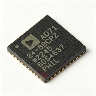
AD5381BSTZ-5 - 40-Channel 12-Bit DAC | Analog Devices
MPN: AD5381BSTZ-5 ✓ Active| Qty | Unit Price | Extended |
|---|---|---|
| 1 | $24.5 | $24.50 |
| 10 | $22.1 | $221.00 |
| 100 | $19.8 | $1,980.00 |
| 500 | $17.6 | $8,800.00 |
| 1,000 | $15.9 | $15,900.00 |
AD5381BSTZ-5 Overview
A digital-to-analog converter (DAC) is an electronic component that converts digital binary data into an analog voltage or current. The AD5381BSTZ-5 is a multi-channel DAC, specifically a denseDAC, designed for systems requiring many precise analog outputs from a single IC. It belongs to the data acquisition product family, which includes ADCs, DACs, and analog front ends, and is essential in industrial control, automated test equipment, and instrumentation where multiple analog voltages must be generated accurately.
Key features include guaranteed monotonic INL error of ±1 LSB max, a 10 ppm/°C on-chip reference, rail-to-rail output amplifiers, and a power-down mode. The device operates over the industrial temperature range of -40°C to +85°C. The 100-lead LQFP package (14x14 mm) provides a compact footprint for high-channel-count designs. The AD5381BSTZ-5 is the 5V supply version; a 3V version (AD5381BSTZ-3) is also available.
Technically, the AD5381 uses a segmented architecture with an internal reference and output amplifiers, ensuring monotonicity and low INL. The channel monitor function allows external monitoring of any channel without disturbing the output, which is valuable for system diagnostics. The serial interface supports daisy-chaining for multiple devices, and the parallel interface allows high-speed updates. The power-down mode reduces current consumption to a low level, beneficial for power-sensitive applications.
Typical applications include industrial process control, automated test equipment (ATE), instrumentation, and multi-channel voltage biasing in optical modules. The 40-channel density and 12-bit resolution make it ideal for systems requiring many accurate analog outputs, such as setting bias voltages in MEMS or optical devices. The rail-to-rail output and single-supply operation simplify power supply design.
When designing with the AD5381BSTZ-5, ensure proper decoupling of the AVDD and DVDD supplies with 0.1µF and 10µF capacitors close to the pins. The reference output should be buffered if driving external loads. For serial mode, tie SER/PAR high and SPI/I2C low. Verify the interface timing against the datasheet to avoid data corruption.
Drop-in alternatives for AD5381BSTZ-5 — same package, pin-to-pin compatible. Different-package parts requiring PCB rework are excluded.
Variants in this series
Same-series models that are drop-in compatible with AD5381BSTZ-5 (same form factor and footprint) — differing in Internal Reference, Supply Voltage, Resolution, Operating Temperature Range, Power-On Reset.
Quick Comparison Tool — Select alternative parts for side-by-side comparison:
AD5381BSTZ-5-REEL
✅ Drop-In📋 Reference alternative (not in catalog)
AD5381BSTZ-3
✅ Drop-In✓ In Stock
$46.83 / Unit
View Datasheet →AD5381BST-5
✅ Drop-In📋 Reference alternative (not in catalog)
AD5381BSTZ-5-REEL7
✅ Drop-In ⚠️ Specs Unverified📋 Reference alternative (not in catalog)
AD5381BSTZ-5-REEL
✅ Drop-In📋 Reference alternative (not in catalog)
AD5381BSTZ-5 Maximum Ratings & Electrical Characteristics
| Number of Channels | 40 |
| Resolution | 12 Bit |
| Supply Voltage | 5 V (single supply) |
| Data Interface | Serial, Parallel |
| Output Type | Voltage - Buffered |
| INL Error | ±1 LSB max |
| Reference Type | Internal, External |
| Internal Reference | 1.25 V / 2.5 V, 10 ppm/°C |
| Operating Temperature | -40°C to +85°C |
| Package / Case | 100-LQFP (14x14 mm) |
| Mounting Type | Surface Mount |
| Packaging | Cut Tape (CT) |
| Output Amplifier | Rail-to-rail |
| Power-Down Mode | Yes |
| Channel Monitor | Yes (MON_OUT pin) |
AD5381BSTZ-5 Pin Configuration
| Pin 1 | VOUT0 — Analog output channel 0 |
| Pin 2 | VOUT1 — Analog output channel 1 |
| Pin 3 | VOUT2 — Analog output channel 2 |
| Pin 4 | VOUT3 — Analog output channel 3 |
| Pin 5 | VOUT4 — Analog output channel 4 |
| Pin 6 | VOUT5 — Analog output channel 5 |
| Pin 7 | VOUT6 — Analog output channel 6 |
| Pin 8 | VOUT7 — Analog output channel 7 |
| Pin 9 | VOUT8 — Analog output channel 8 |
| Pin 10 | VOUT9 — Analog output channel 9 |
| Pin 11 | VOUT10 — Analog output channel 10 |
| Pin 12 | VOUT11 — Analog output channel 11 |
| Pin 13 | VOUT12 — Analog output channel 12 |
| Pin 14 | VOUT13 — Analog output channel 13 |
| Pin 15 | VOUT14 — Analog output channel 14 |
| Pin 16 | VOUT15 — Analog output channel 15 |
| Pin 17 | VOUT16 — Analog output channel 16 |
| Pin 18 | VOUT17 — Analog output channel 17 |
| Pin 19 | VOUT18 — Analog output channel 18 |
| Pin 20 | VOUT19 — Analog output channel 19 |
| Pin 21 | VOUT20 — Analog output channel 20 |
| Pin 22 | VOUT21 — Analog output channel 21 |
| Pin 23 | VOUT22 — Analog output channel 22 |
| Pin 24 | VOUT23 — Analog output channel 23 |
| Pin 25 | VOUT24 — Analog output channel 24 |
| Pin 26 | VOUT25 — Analog output channel 25 |
| Pin 27 | VOUT26 — Analog output channel 26 |
| Pin 28 | VOUT27 — Analog output channel 27 |
| Pin 29 | VOUT28 — Analog output channel 28 |
| Pin 30 | VOUT29 — Analog output channel 29 |
| Pin 31 | VOUT30 — Analog output channel 30 |
| Pin 32 | VOUT31 — Analog output channel 31 |
| Pin 33 | VOUT32 — Analog output channel 32 |
| Pin 34 | VOUT33 — Analog output channel 33 |
| Pin 35 | VOUT34 — Analog output channel 34 |
| Pin 36 | VOUT35 — Analog output channel 35 |
| Pin 37 | VOUT36 — Analog output channel 36 |
| Pin 38 | VOUT37 — Analog output channel 37 |
| Pin 39 | VOUT38 — Analog output channel 38 |
| Pin 40 | VOUT39 — Analog output channel 39 |
| Pin 41 | AVDD — Analog supply voltage |
| Pin 42 | AGND — Analog ground |
| Pin 43 | DVDD — Digital supply voltage |
| Pin 44 | DGND — Digital ground |
| Pin 45 | REFIN/REFOUT — Reference input/output |
| Pin 46 | MON_OUT — Channel monitor output |
| Pin 47 | SER/PAR — Serial/parallel interface select |
| Pin 48 | SPI/I2C — SPI or I2C select (Pin 97) |
| Pin 49 | SCLK — Serial clock input |
| Pin 50 | SDIN — Serial data input |
| Pin 51 | SYNC — Frame synchronization input |
| Pin 52 | SDO — Serial data output |
| Pin 53 | LDAC — Load DAC latch |
| Pin 54 | CLR — Clear all DACs to zero-scale |
| Pin 55 | PD — Power-down input |
| Pin 56 | RESET — Reset to default state |
| Pin 57 | A0-A9 — Address inputs for parallel mode |
| Pin 58 | D0-D11 — Parallel data inputs |
| Pin 59 | CS — Chip select |
| Pin 60 | WR — Write strobe |
| Pin 61 | RD — Read strobe |
| Pin 62 | BUSY — Busy indicator |
| Pin 63 | VLOGIC — Logic supply voltage |
| Pin 64 | NC — No connect |
Typical Applications
AD5381BSTZ-5 is suitable for 6 applications: Industrial Process Control, Automated Test Equipment (ATE), Instrumentation, Optical Module Bias, Medical Instrumentation, Audio Test and Measurement.
Industrial Process Control
The AD5381BSTZ-5 provides 40 channels of 12-bit analog output for controlling valves, actuators, and setpoints in industrial process control systems. Its rail-to-rail output and single 5V supply simplify interfacing with industrial sensors and actuators. The channel monitor function allows real-time diagnostics of each output without disturbing the control loop. With an INL of ±1 LSB, it ensures precise setpoint accuracy, critical for maintaining process stability. The industrial temperature range (-40°C to +85°C) ensures reliable operation in harsh factory environments.
Recommended
Automated Test Equipment (ATE)
In ATE, the AD5381BSTZ-5 generates multiple precision bias voltages and stimulus signals for testing DUTs. Its 40-channel density reduces board space and cost compared to using multiple lower-channel DACs. The serial interface supports daisy-chaining for even more channels, and the parallel interface enables high-speed updates for dynamic testing. The internal reference with 10 ppm/°C drift provides stable voltages over temperature, ensuring test repeatability. The power-down mode helps reduce heat in dense test systems.
Recommended
Instrumentation
The AD5381BSTZ-5 is ideal for precision instrumentation requiring multiple analog outputs, such as calibrators, signal generators, and data acquisition systems. Its 12-bit resolution and low INL ensure accurate output voltages. The rail-to-rail output allows full-scale swings, maximizing dynamic range. The channel monitor function enables self-test and calibration routines. The compact 100-lead LQFP package fits space-constrained designs, and the single-supply operation simplifies power design.
Recommended
Optical Module Bias
The AD5381BSTZ-5 provides multiple bias voltages for optical transceivers, such as MZM bias control and APD bias. Its 40 channels can individually set bias points for multiple optical components, reducing component count. The low drift internal reference ensures stable bias over temperature, critical for optical performance. The serial interface allows easy configuration from a microcontroller. The power-down mode reduces power consumption when channels are not in use.
Recommended
Medical Instrumentation
In medical devices like patient monitors and diagnostic equipment, the AD5381BSTZ-5 generates precise analog voltages for sensor excitation and control. Its 40 channels can drive multiple transducers, and the rail-to-rail output ensures full-scale signals. The industrial temperature range covers medical environments. The channel monitor function aids in fault detection, enhancing patient safety. The low power consumption in power-down mode is beneficial for battery-operated devices.
Recommended
Audio Test and Measurement
The AD5381BSTZ-5 can generate multiple DC bias voltages for audio test systems, such as setting operating points for amplifiers or attenuators. Its 12-bit resolution provides fine voltage steps, and the low noise output is suitable for audio applications. The serial interface allows easy integration with DSPs. The channel monitor function enables verification of output voltages during test. The compact package is ideal for portable test equipment.
Recommended
Recommended Products Summary
Engineering reference data for AD5381BSTZ-5 — comparison, design guidance, and compliance information.
Selection Guide
Comparison with Alternatives
| Parameter | This Product | AD5381BSTZ-5-REEL | AD5381BSTZ-3 | AD5381BST-5 |
|---|---|---|---|---|
| Package | 100-LQFP (14x14 mm) | 100-LQFP (14x14 mm) - same | 100-LQFP (14x14 mm) - same | 100-LQFP (14x14 mm) - same |
| Brand | Analog Devices | Analog Devices | Analog Devices | Analog Devices |
| Supply Voltage | 5V | 5V | 3V | 5V |
| Resolution | 12-bit | 12-bit | 12-bit | 12-bit |
| Number of Channels | 40 | 40 | 40 | 40 |
| INL Error | ±1 LSB max | ±1 LSB max | ±1 LSB max | ±1 LSB max |
| Internal Reference | 1.25V/2.5V, 10 ppm/°C | 1.25V/2.5V, 10 ppm/°C | 1.25V/2.5V, 10 ppm/°C | 1.25V/2.5V, 10 ppm/°C |
| Operating Temperature | -40°C to +85°C | -40°C to +85°C | -40°C to +85°C | -40°C to +85°C |
Key Differentiators
- 40-channel density in a single package (vs AD5381BSTZ-3)
- 5V single-supply operation (vs AD5381BSTZ-3)
- On-chip channel monitor (vs AD5381BSTZ-5-REEL)
Design Notes
Decouple AVDD and DVDD with 0.1µF and 10µF capacitors placed as close to the pins as possible. Use separate analog and digital ground planes to minimize noise coupling. The AD5381 operates from a single 5V supply; ensure the supply is clean and stable to maintain DAC accuracy.
For the 100-lead LQFP package, ensure proper solder paste stencil design to avoid bridging. Use a thermal pad if available for heat dissipation. Route analog outputs away from digital traces to reduce crosstalk. Follow the layout guidelines in the AD5381 datasheet for optimal performance.
When using serial mode, tie SER/PAR high and SPI/I2C low (Pin 97). Ensure the interface timing meets the datasheet specifications to avoid data corruption. The internal reference output should be buffered if driving external loads. Do not exceed the absolute maximum ratings for supply voltage.
Compliance Information
The 'Z' suffix in AD5381BSTZ-5 indicates lead-free (RoHS compliant) per Analog Devices naming convention. REACH and conflict minerals status not specified in provided data.