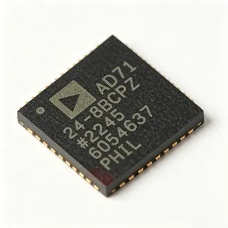
AD561SD/883B - 10-Bit Monolithic DAC | Analog Devices
MPN: AD561SD/883B ✓ Active| Qty | Unit Price | Extended |
|---|---|---|
| 1 | $45.32 | $45.32 |
| 10 | $41.87 | $418.70 |
| 100 | $38.45 | $3,845.00 |
| 500 | $35.02 | $17,510.00 |
| 1,000 | $31.6 | $31,600.00 |
AD561SD/883B Overview
A digital-to-analog converter (DAC) is an electronic component that converts digital binary data into an analog voltage or current. The AD561SD/883B is a current-output DAC, meaning it outputs a current proportional to the digital input, which can be converted to a voltage using an external op-amp. DACs are fundamental building blocks in data acquisition systems, where they generate analog signals for control, waveform generation, and audio applications. The AD561SD/883B belongs to the family of precision DACs, offering 10-bit resolution and a built-in reference, simplifying system design.
Key features of the AD561SD/883B include its 10-bit resolution, monolithic construction with integrated voltage reference, and military-grade screening. The device operates over the full military temperature range of -55°C to +125°C, making it suitable for aerospace and defense applications. The hermetically sealed ceramic DIP package ensures reliability in harsh environments. The laser-trimmed thin-film resistor network provides excellent linearity and accuracy, with a typical settling time of and a gain error of .
The AD561SD/883B is designed for high-performance applications where precision and reliability are critical. Its current output can be easily converted to a voltage using an external operational amplifier, and the integrated reference eliminates the need for an external reference source. The device is pin-compatible with other members of the AD561 family, allowing for easy upgrades or replacements. The military-grade screening ensures compliance with stringent quality standards, making it ideal for mission-critical systems.
Typical applications include military avionics, radar systems, industrial process control, and test and measurement equipment. The wide operating temperature range and hermetically sealed package make it suitable for extreme environments. When designing with the AD561SD/883B, ensure proper decoupling on the power supply pins and consider the output current-to-voltage conversion circuit to achieve optimal performance.
Drop-in alternatives for AD561SD/883B — same package, pin-to-pin compatible. Different-package parts requiring PCB rework are excluded.
Variants in this series
Same-series models that are drop-in compatible with AD561SD/883B (same form factor and footprint) — differing in Output Type.
Quick Comparison Tool — Select alternative parts for side-by-side comparison:
AD561SD
✅ Drop-In📋 Reference alternative (not in catalog)
AD561SD/883B Maximum Ratings & Electrical Characteristics
| Resolution | 10 bit |
| Number of Channels | 1 |
| Architecture | R-2R |
| Output Type | Current |
| Reference Type | Internal |
| Operating Temperature Range | -55°C to +125°C |
| Package Type | 16-pin CDIP (Ceramic DIP) |
| Mounting Style | Through Hole |
| Screening Level | Military |
| RoHS Status | unknown |
AD561SD/883B Pin Configuration
| Pin 1 | VREF — Voltage reference output |
| Pin 2 | VREF — Voltage reference output |
| Pin 3 | GND — Ground |
| Pin 4 | BIT1 (MSB) — Most significant bit input |
| Pin 5 | BIT2 — Digital input bit 2 |
| Pin 6 | BIT3 — Digital input bit 3 |
| Pin 7 | BIT4 — Digital input bit 4 |
| Pin 8 | BIT5 — Digital input bit 5 |
| Pin 9 | BIT6 — Digital input bit 6 |
| Pin 10 | BIT7 — Digital input bit 7 |
| Pin 11 | BIT8 — Digital input bit 8 |
| Pin 12 | BIT9 — Digital input bit 9 |
| Pin 13 | BIT10 (LSB) — Least significant bit input |
| Pin 14 | VEE — Negative supply voltage |
| Pin 15 | IOUT — Current output |
| Pin 16 | VCC — Positive supply voltage |
Typical Applications
AD561SD/883B is suitable for 6 applications: Military Avionics, Radar Systems, Industrial Process Control, Test and Measurement Equipment, Aerospace Data Acquisition, Medical Instrumentation.
Military Avionics
The AD561SD/883B is ideal for military avionics systems due to its military-grade screening and wide operating temperature range of -55°C to +125°C. Its 10-bit resolution and internal reference provide precise analog output for flight control and navigation systems. The hermetically sealed ceramic DIP package ensures reliability in harsh environments, making it suitable for mission-critical applications where failure is not an option.
Recommended
Radar Systems
In radar systems, the AD561SD/883B generates precise analog control voltages for beam steering and signal processing. Its fast settling time and low glitch energy ensure accurate waveform generation. The military temperature range and hermetic package make it suitable for airborne and ground-based radar installations. The integrated reference simplifies design, reducing component count and improving system reliability.
Recommended
Industrial Process Control
The AD561SD/883B is used in industrial process control for generating analog setpoints and control signals. Its 10-bit resolution provides fine granularity for precise adjustments. The wide operating temperature range allows deployment in factory floors with extreme conditions. The current output can directly drive actuators or be converted to voltage for PLC interfaces. The device's reliability ensures minimal downtime in continuous operation.
Recommended
Test and Measurement Equipment
The AD561SD/883B is well-suited for test and measurement equipment such as waveform generators and calibration instruments. Its 10-bit resolution and internal reference ensure accurate and stable output. The military-grade screening guarantees long-term stability and repeatability, essential for calibration standards. The through-hole package is easy to integrate into benchtop instruments, and the wide temperature range allows use in environmental test chambers.
Recommended
Aerospace Data Acquisition
In aerospace data acquisition systems, the AD561SD/883B converts digital commands to analog signals for controlling actuators and sensors. Its military temperature range and hermetic package are essential for space and high-altitude applications. The integrated reference reduces external component count, saving board space and improving reliability. The device's fast settling time enables high-speed data updates, critical for real-time control.
Recommended
Medical Instrumentation
The AD561SD/883B can be used in medical instrumentation for generating precise analog signals in diagnostic equipment. Its 10-bit resolution and low noise ensure accurate signal generation. The wide temperature range allows use in sterilization environments. The hermetically sealed package protects against moisture and contaminants, making it suitable for medical devices that require high reliability. The internal reference simplifies calibration.
Recommended
Recommended Products Summary
Engineering reference data for AD561SD/883B — comparison, design guidance, and compliance information.
Selection Guide
Comparison with Alternatives
| Parameter | This Product | AD561SD | AD561JNZ | AD561KNZ |
|---|---|---|---|---|
| Resolution | 10 bit | 10 bit | 10 bit | 10 bit |
| Package | 16-pin CDIP | 16-pin CDIP | 16-pin PDIP | 16-pin PDIP |
| Temperature Range | -55°C to +125°C | -55°C to +125°C | 0°C to +70°C | 0°C to +70°C |
| Screening Level | Military | Military | Commercial | Commercial |
| Reference Type | Internal | Internal | Internal | Internal |
| Output Type | Current | Current | Current | Current |
| Brand | Analog Devices | Analog Devices | Analog Devices | Analog Devices |
Key Differentiators
- Military-grade screening (vs AD561JNZ)
- Hermetic ceramic package (vs AD561KNZ)
- Wide temperature range (vs AD561JNZ)
Design Notes
The AD561SD/883B requires a positive and negative supply voltage for proper operation. Ensure that the VCC and VEE pins are adequately decoupled with 0.1uF ceramic capacitors placed close to the pins. The supply voltages should be stable and within the recommended range to avoid output errors. Refer to the datasheet for exact supply voltage specifications.
For optimal performance, use a ground plane on the PCB to minimize noise and parasitic inductance. Keep digital and analog grounds separate and connect them at a single point. Place the output current-to-voltage conversion op-amp close to the IOUT pin to reduce stray capacitance. Use short, direct traces for the digital input lines to avoid crosstalk.
Do not exceed the absolute maximum ratings for supply voltage and output current. Ensure that the digital input voltages are within the specified logic levels to prevent damage. When converting the current output to voltage, use a precision op-amp with low offset voltage and low input bias current to maintain accuracy. Also, consider the output capacitance and its effect on settling time.
Compliance Information
Compliance information not provided in the verified data. The AD561SD/883B is a military-grade component, and RoHS status may not apply due to exemptions for military applications.