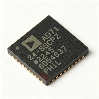
AD7949BCPZRL7 - 14-Bit 8-Ch 250kSPS SAR ADC | Analog Devices
MPN: AD7949BCPZRL7 ✓ Active| Qty | Unit Price | Extended |
|---|---|---|
| 1 | $8.4432 | $8.44 |
| 10 | $7.6 | $76.00 |
| 100 | $6.75 | $675.00 |
| 500 | $6.3 | $3,150.00 |
| 1,000 | $6.2 | $6,200.00 |
AD7949BCPZRL7 Overview
A SAR ADC is a class of analog-to-digital converter that converts an analog input into a digital code using a binary-search algorithm implemented with a capacitive charge-redistribution DAC. It samples the input, holds it on an internal capacitor array, and iteratively compares it against a reference voltage. SAR ADCs are valued for high speed, deterministic latency (no pipeline delay), low power, and ease of use, making them ideal for applications requiring moderate resolution and high throughput without the latency of delta-sigma converters. In the broader taxonomy, the AD7949 sits as: SAR ADC -> ADC -> data converter -> signal chain IC -> mixed-signal semiconductor.
Key features include 14-bit resolution with no missing codes, 250 kSPS throughput, +/-1 LSB typical INL, and a serial SPI-compatible interface with clock rates up to 50 MHz. A daisy-chain mode allows multiple AD7949 devices to share one serial bus, simplifying system expansion. Power dissipation is 4.5 mW typical at 5 V / 250 kSPS, dropping to 1 uA in power-down mode for battery-friendly operation. The device accepts an external reference from 2.3 V to 5.5 V (matching VDD) and includes an internal reference buffer.
The AD7949 architecture uses a differential analog input structure with a track-and-hold amplifier that acquires the input in 290 ns, ensuring accurate conversion at full throughput. The 20-lead LFCSP (4x4 mm) package exposes the thermal pad to the PCB ground plane for thermal relief and provides a compact footprint suitable for high-density designs. Per the AD7949 datasheet, the part is pin-to-pin compatible with the 16-bit AD7682, AD7689, and AD7699, allowing resolution upgrades on existing boards.
Typical applications include multichannel data acquisition systems, industrial process control, medical instrumentation, battery-powered portable instruments, and programmable logic controller (PLC) analog input modules. The wide 2.3 V to 5.5 V supply range supports direct interfacing to 3.3 V or 5 V microcontrollers without level shifters.
When designing with the AD7949, ensure the reference voltage source is low-noise and well-decoupled, since reference accuracy directly limits conversion accuracy. Drive analog inputs with a low-impedance source (an op-amp buffer or dedicated ADC driver) and place a 10 nF (minimum) capacitor directly at the REF pin to filter high-frequency noise. Keep the serial SPI traces short and away from noisy switching traces to maintain signal integrity at 50 MHz clock rates.
This page synthesizes distributor pricing, verified pin-to-pin drop-in alternatives, and practical design notes not found in the manufacturer datasheet.
Drop-in alternatives for AD7949BCPZRL7 — same package, pin-to-pin compatible. Different-package parts requiring PCB rework are excluded.
Variants in this series
Same-series models that are drop-in compatible with AD7949BCPZRL7 (same form factor and footprint) — differing in Package, Input Type, Resolution, Interface, Operating Temperature.
Quick Comparison Tool — Select alternative parts for side-by-side comparison:
AD7949BCPZ
✅ Drop-In📋 Reference alternative (not in catalog)
AD7682BCPZ
✅ Drop-In✓ In Stock
$4.98 / Unit
View Datasheet →AD7689BCPZ
✅ Drop-In📋 Reference alternative (not in catalog)
AD7699BCPZ
✅ Drop-In✓ In Stock
$8.05 / Unit
View Datasheet →AD7946BCPZ
✅ Drop-In✓ In Stock
$9.5 / Unit
View Datasheet →AD7685BCPZ
✅ Drop-In✓ In Stock
$8.1 / Unit
View Datasheet →AD7949BCPZRL7 Maximum Ratings & Electrical Characteristics
| Resolution | 14 bit |
| Number of Channels | 8 (single-ended) / 4 (differential pairs) |
| Architecture | SAR (Successive Approximation Register) |
| Sample Rate | 250 kSPS |
| Input Type | Single-Ended, Pseudobipolar, Differential (GND sense) |
| Supply Voltage (VDD) | 2.3 V to 5.5 V |
| Reference Voltage | 2.3 V to 5.5 V (external) |
| INL (Integral Nonlinearity) | +/-1 LSB (typical) |
| No Missing Codes | Yes (14-bit guaranteed) |
| Digital Interface | SPI / QSPI / MICROWIRE / DSP-compatible, up to 50 MHz |
| Daisy-Chain Mode | Yes |
| Power Dissipation (250 kSPS, 5 V) | 4.5 mW (typical) |
| Power-Down Current | 1 uA (typical) |
| Acquisition Time | 290 ns (typical) |
| Operating Temperature | -40C to +125C |
| Package | 20-LFCSP (4x4 mm) with exposed pad |
| Mounting Type | Surface Mount |
| RoHS Status | Compliant |
AD7949BCPZRL7 Pin Configuration
| Pin 1 | VDD — Power supply input (2.3 V to 5.5 V) |
| Pin 2 | VDDIO — Digital I/O supply (1.8 V to 5.5 V) |
| Pin 3 | GND — Ground |
| Pin 4 | REF — Reference voltage input (decouple with 10 nF min) |
| Pin 5 | REFGND — Reference ground return |
| Pin 6 | IN0 — Analog input channel 0 |
| Pin 7 | IN1 — Analog input channel 1 |
| Pin 8 | IN2 — Analog input channel 2 |
| Pin 9 | IN3 — Analog input channel 3 |
| Pin 10 | IN4 — Analog input channel 4 |
| Pin 11 | IN5 — Analog input channel 5 |
| Pin 12 | IN6 — Analog input channel 6 |
| Pin 13 | IN7 — Analog input channel 7 |
| Pin 14 | GND — Ground |
| Pin 15 | SDO — Serial data output (SPI MISO) |
| Pin 16 | SDI — Serial data input (SPI MOSI, for daisy-chain) |
| Pin 17 | SCK — Serial clock input (up to 50 MHz) |
| Pin 18 | CNV — Conversion start input (active low) |
| Pin 19 | BUSY — Conversion busy output (active high) |
| Pin 20 | NC — Not connected (per datasheet) |
Typical Applications
AD7949BCPZRL7 is suitable for 6 applications: Multichannel Data Acquisition System, Industrial Process Control, Medical Instrumentation, Battery-Powered Portable Instrumentation, PLC Analog Input Module, Data Logger / Embedded Sensor Hub.
Multichannel Data Acquisition System
The AD7949BCPZRL7's 8-channel input multiplexer and 14-bit / 250 kSPS throughput make it an excellent single-IC solution for multichannel data acquisition. With +/-1 LSB typical INL and no-missing-codes guarantee, it accurately digitizes signals from multiple sensors without cross-channel latency. Typical circuit: AD7949 in series with a precision 5V reference (ADR435) and driven by an AD8628 op-amp buffer at each analog input. The SPI interface connects to an STM32 or similar MCU. Compared to running 8 separate ADCs, this design reduces board area, BOM cost, and synchronization complexity while maintaining 4.5 mW total power at full speed. The exposed thermal pad aids heat dissipation at high throughput.
Recommended
Industrial Process Control
Industrial process control loops demand reliable, low-latency analog measurement of temperature, pressure, flow, and level signals. The AD7949BCPZRL7's deterministic SAR architecture (no pipeline delay) provides immediate conversion results ideal for PID feedback. The 2.3 V to 5.5 V supply simplifies integration into 24V-bus-derived 5V or 3.3V rails, and the -40C to +125C operating range supports harsh factory environments. The 8-channel mux allows a single ADC to monitor multiple 4-20 mA current loops (via shunt resistors) or 0-10V sensor outputs (via resistor dividers). Daisy-chain SPI mode lets engineers scale to 16, 24, or 32 channels by stacking multiple AD7949 devices on one bus, preserving MCU pin count.
Recommended
Medical Instrumentation
Patient monitoring and portable medical devices require compact, low-power, high-accuracy ADCs. The AD7949BCPZRL7's 4.5 mW active power and 1 uA power-down current extend battery life in handheld ECG, pulse oximeter, and blood-pressure monitor designs. The 14-bit resolution is sufficient for diagnostic-grade biosignal acquisition when paired with low-noise analog front ends. The 20-LFCSP (4x4 mm) package fits inside miniaturized enclosures, and the SPI interface is straightforward for ARM Cortex-M0/M4 class MCUs. Compliance with the -40C to +125C industrial temperature range (rather than medical-specific 0C to +70C) gives designers flexibility for non-clinical variants.
Recommended
Battery-Powered Portable Instrumentation
Field-portable instruments such as handheld multimeters, environmental loggers, and wireless sensor nodes depend on microamp-level standby current. The AD7949BCPZRL7 consumes only 1 uA in power-down mode, allowing the MCU to duty-cycle conversions and spend most of its time asleep. The 2.3 V minimum supply supports direct operation from a single Li-ion cell (3.0 V to 4.2 V) without boost or LDO regulators. The wide operating temperature range enables outdoor deployment. The 8 input channels permit connection to multiple sensor types (temperature, humidity, gas, vibration) through one ADC, reducing total BOM and PCB area in space-constrained handheld enclosures.
Recommended
PLC Analog Input Module
Programmable logic controller (PLC) analog input modules typically handle 4, 8, or 16 channels of +/-10 V or 0-10 V signals. The AD7949BCPZRL7's 8-channel mux and pseudobipolar input capability support cost-effective 8-channel modules. Resistor dividers scale high-voltage signals into the 0-VREF ADC range, while the SPI interface streams data to the PLC's main processor. The wide supply range (2.3 V to 5.5 V) accommodates both 3.3 V and 5 V PLC backplanes. Industrial temperature rating (-40C to +125C) ensures operation in factory cabinets. Multiple AD7949 devices can be daisy-chained for 16-channel and 32-channel modules without additional GPIO pins.
Recommended
Data Logger / Embedded Sensor Hub
Embedded data loggers for HVAC, building automation, and asset tracking use compact ADCs to sample environmental and operational sensors. The AD7949BCPZRL7's 250 kSPS throughput allows oversampling techniques to push effective resolution beyond 14 bits when bandwidth permits. The 8 channels connect to thermocouples (with cold-junction compensation via separate temperature sensor), strain gauges, and 4-20 mA loop sensors. The small 20-LFCSP (4x4 mm) footprint fits on daughter boards inside tight enclosures. The SPI interface is supported by virtually every modern MCU family, simplifying firmware development and BOM selection.
Recommended
Recommended Products Summary
Engineering reference data for AD7949BCPZRL7 — comparison, design guidance, and compliance information.
Selection Guide
Comparison with Alternatives
| Parameter | This Product | AD7949BCPZ | AD7682BCPZ | AD7689BCPZ | AD7699BCPZ | AD7946BCPZ | AD7685BCPZ |
|---|---|---|---|---|---|---|---|
| Brand | Analog Devices | Analog Devices | Analog Devices | Analog Devices | Analog Devices | Analog Devices | Analog Devices |
| Package | 20-LFCSP (4x4) | 20-LFCSP (4x4) - same | 20-LFCSP (4x4) - same | 20-LFCSP (4x4) - same | 20-LFCSP (4x4) - same | 20-LFCSP (4x4) - same | 20-LFCSP (4x4) - same |
| Resolution | 14 bit | 14 bit | 16 bit | 16 bit | 16 bit | 14 bit | 16 bit |
| Sample Rate | 250 kSPS | 250 kSPS | 250 kSPS | 250 kSPS | 500 kSPS | 500 kSPS | 250 kSPS |
| Number of Channels | 8 | 8 | 4 | 8 | 8 | 8 | 1 |
| Supply Voltage | 2.3 V to 5.5 V | 2.3 V to 5.5 V | 2.3 V to 5.5 V | 2.3 V to 5.5 V | 2.3 V to 5.5 V | 2.3 V to 5.5 V | 2.3 V to 5.5 V |
| INL (typical) | +/-1 LSB | +/-1 LSB | +/-1 LSB | +/-1 LSB | +/-1 LSB | +/-1 LSB | +/-1 LSB |
| Power @ full speed | 4.5 mW | 4.5 mW | 4.5 mW | 4.5 mW | 9 mW | 9 mW | 4.5 mW |
| Operating Temperature | -40C to +125C | -40C to +125C | -40C to +125C | -40C to +125C | -40C to +85C | -40C to +125C | -40C to +125C |
Key Differentiators
- Only 14-bit 8-channel SAR ADC with this exact footprint and pinout (vs AD7946BCPZ)
- Truly pin-compatible 16-bit upgrade path on the same PCB (vs AD7699BCPZ / AD7689BCPZ / AD7682BCPZ)
- 8 channels integrated vs external multiplexer required (vs AD7685BCPZ)
Design Notes
Reference decoupling is critical for AD7949 conversion accuracy. Place a 10 nF (minimum) ceramic capacitor as close as physically possible to the REF pin, with short traces to REFGND. Reference noise directly couples into conversion results at the LSB level - a 5 uVrms reference noise degrades a 14-bit, 5V-full-scale conversion by approximately 0.3 LSB. For best performance, use a low-noise reference such as ADR435 or ADR4550 and add a bulk 1 uF to 10 uF capacitor in parallel with the 10 nF.
Route analog and digital sections on separate PCB regions with a star-ground connection at the AD7949 GND pin (or the LFCSP exposed pad). The exposed thermal pad MUST be soldered to the PCB ground plane for thermal relief and electrical return. Keep the SPI traces (SCK, SDO, SDI, CNV, BUSY) short and routed away from the analog inputs and reference traces to avoid digital noise coupling into the analog path. Use a 4-layer PCB if possible to provide a solid ground plane beneath the ADC.
Drive the AD7949 analog inputs with a low-impedance source (op-amp buffer such as AD8628 or ADA4522) capable of settling within the 290 ns acquisition window. Source impedances above 1 kOhm will introduce gain errors and distortion due to the ADC input sampling current transients. For multiplexed inputs, the buffer must settle within the MUX switching time plus the ADC acquisition time at full throughput. Series resistors (>10 Ohm) between buffer and ADC input should be avoided unless paired with a 10 nF capacitor at the ADC pin to form a low-pass filter.
Do not leave the CNV pin floating - it must be tied high through a pull-up resistor to VDDIO or driven by the MCU. The BUSY pin indicates conversion status and must be monitored or the MCU must observe the datasheet's minimum conversion time before reading SDO. For daisy-chain mode, ensure SCK stays low when CNV is low; clocking SCK during conversion start causes corruption. Always issue a dummy conversion after power-up to reset the internal sample capacitor state before relying on conversion accuracy.
Compliance Information
RoHS compliant per Analog Devices product page. Industrial temperature grade (-40C to +125C); not AEC-Q100 automotive qualified - choose automotive-grade variants separately if required.