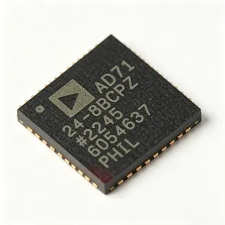
AD90585 - Dual 8-Bit 50 MSPS ADC | Analog Devices
MPN: AD90585 ✓ Active| Qty | Unit Price | Extended |
|---|---|---|
| 1 | $25 | $25.00 |
| 10 | $22.5 | $225.00 |
| 100 | $20 | $2,000.00 |
| 500 | $18 | $9,000.00 |
| 1,000 | $16 | $16,000.00 |
AD90585 Overview
An analog-to-digital converter (ADC) is a critical building block in digital signal processing chains, converting continuous analog signals into discrete digital values for processing by microcontrollers, DSPs, or FPGAs. The AD90585 belongs to the family of high-speed flash ADCs, which use a parallel comparator architecture to achieve very high sampling rates. This architecture is ideal for applications requiring wide bandwidth and low latency, such as radar, communications, and medical imaging.
Key features of the AD90585 include two matched ADCs on a single chip, ensuring excellent channel-to-channel matching for applications like quadrature demodulation. The device offers a low power consumption of less than 1W, making it suitable for portable and power-sensitive designs. The low input capacitance of 10 pF minimizes loading on the driving amplifier, preserving signal integrity. The on-board voltage reference provides a stable and accurate reference, eliminating the need for an external reference in many designs.
The AD90585 uses a flash architecture with a resistor ladder and comparator bank, achieving high-speed conversion with minimal latency. The device includes a reference ladder offset feature, which uses 2 kΩ pull-down resistors on the output data bits to equalize rise and fall times at high conversion rates, easing data latching into external logic. This design consideration is critical for reliable operation above 40 MSPS.
Typical applications include quadrature demodulation for communications, digital oscilloscopes, and other high-speed data acquisition systems. The dual-channel architecture is particularly advantageous in I/Q demodulation, where two matched ADCs are required to process in-phase and quadrature components simultaneously. The low power and small footprint make it suitable for embedded systems and portable instrumentation.
When designing with the AD90585, ensure that the analog input is properly buffered and that the reference ladder offset resistors are included for high-speed operation. The device requires careful PCB layout to minimize parasitic capacitance and maintain signal integrity. The ±5V supplies should be well-decoupled to avoid noise coupling into the analog input.
Drop-in alternatives for AD90585 — same package, pin-to-pin compatible. Different-package parts requiring PCB rework are excluded.
Quick Comparison Tool — Select alternative parts for side-by-side comparison:
AD9058AKD
✅ Drop-In📋 Reference alternative (not in catalog)
AD9058AKJ
✅ Drop-In📋 Reference alternative (not in catalog)
AD9058ATD/883B
✅ Drop-In📋 Reference alternative (not in catalog)
AD9058
✅ Drop-In📋 Reference alternative (not in catalog)
AD90585 Maximum Ratings & Electrical Characteristics
| Number of ADCs | 2 |
| Resolution | 8 bit |
| Sampling Rate | 50 MSPS |
| Architecture | Flash |
| Input Voltage Range | Flexible |
| Supply Voltage | ±5 V |
| Power Dissipation | <1 W |
| Input Capacitance | 10 pF |
| On-Board Voltage Reference | Yes |
| Reference Ladder Offset | 2 kΩ pull-down resistors on D0-D7 |
| Package Type | 44-JLCC (16.39x16.39) |
| Mounting Type | Surface Mount |
AD90585 Pin Configuration
| Pin 1 | D0A — Data output bit 0 for ADC A |
| Pin 2 | D1A — Data output bit 1 for ADC A |
| Pin 3 | D2A — Data output bit 2 for ADC A |
| Pin 4 | D3A — Data output bit 3 for ADC A |
| Pin 5 | D4A — Data output bit 4 for ADC A |
| Pin 6 | D5A — Data output bit 5 for ADC A |
| Pin 7 | D6A — Data output bit 6 for ADC A |
| Pin 8 | D7A — Data output bit 7 for ADC A |
| Pin 9 | VREF — Voltage reference input/output |
| Pin 10 | VCC — Positive supply (+5V) |
| Pin 11 | GND — Ground |
| Pin 12 | VEE — Negative supply (-5V) |
Typical Applications
AD90585 is suitable for 6 applications: Quadrature Demodulation, Digital Oscilloscopes, Communications Receivers, Medical Imaging, Radar Systems, Test and Measurement.
Quadrature Demodulation
The AD90585's dual matched ADCs are ideal for I/Q demodulation in communications systems. The two channels can simultaneously sample the in-phase and quadrature components, ensuring phase coherence. With 50 MSPS sampling and low input capacitance, it preserves signal integrity for wideband signals. The on-board reference simplifies design, and the low power (<1W) is suitable for portable receivers.
Recommended
Digital Oscilloscopes
In digital oscilloscopes, the AD90585 provides high-speed dual-channel acquisition for simultaneous waveform capture. The 8-bit resolution and 50 MSPS sampling rate allow for accurate representation of fast signals. The low input capacitance minimizes probe loading, and the flexible input range accommodates various signal levels. The dual channels enable differential measurements or simultaneous capture of two signals.
Recommended
Communications Receivers
The AD90585 is well-suited for communications receivers requiring dual-channel digitization. Its 50 MSPS sampling rate supports IF sampling in software-defined radios. The matched ADCs ensure consistent gain and phase response across channels, critical for diversity reception. The low power consumption is beneficial for battery-operated devices, and the on-board reference reduces external component count.
Recommended
Medical Imaging
In medical imaging systems, the AD90585 can be used for high-speed data acquisition from sensors or transducers. The dual channels allow simultaneous sampling of multiple signals, improving throughput. The 8-bit resolution is sufficient for many imaging modalities, and the low power dissipation is advantageous for portable devices. The small package footprint enables compact designs.
Recommended
Radar Systems
The AD90585 is suitable for radar systems requiring high-speed digitization of return signals. The dual channels can process I/Q data for Doppler processing. The 50 MSPS sampling rate captures fast-moving targets, and the low input capacitance preserves signal fidelity. The device's robust performance in harsh environments makes it a reliable choice for defense applications.
Recommended
Test and Measurement
In test and measurement equipment, the AD90585 provides high-speed data acquisition for waveform analysis. The dual channels enable simultaneous measurement of two signals, useful for phase or frequency comparison. The 8-bit resolution is adequate for many test applications, and the flexible input range allows direct connection to various signal sources. The low power consumption is beneficial for portable instruments.
Recommended
Recommended Products Summary
Engineering reference data for AD90585 — comparison, design guidance, and compliance information.
Selection Guide
Comparison with Alternatives
| Parameter | This Product | AD9058AKD | AD9058AKJ | AD9058ATD/883B | AD9058 |
|---|---|---|---|---|---|
| Package | 44-JLCC | 44-JLCC | 44-JLCC | 44-JLCC | 44-JLCC |
| Brand | Analog Devices | Analog Devices | Analog Devices | Analog Devices | Analog Devices |
| Resolution | 8 bit | 8 bit | 8 bit | 8 bit | 8 bit |
| Sampling Rate | 50 MSPS | 50 MSPS | 50 MSPS | 50 MSPS | 50 MSPS |
| Number of ADCs | 2 | 2 | 2 | 2 | 2 |
| Supply Voltage | ±5 V | ±5 V | ±5 V | ±5 V | ±5 V |
| Power Dissipation | <1 W | <1 W | <1 W | <1 W | <1 W |
| Input Capacitance | 10 pF | 10 pF | 10 pF | 10 pF | 10 pF |
Key Differentiators
- Dual matched ADCs on a single chip (vs Single-channel ADCs)
- Low power consumption (<1W) (vs Higher-power dual ADCs)
- On-board voltage reference (vs ADCs requiring external reference)
Design Notes
The AD90585 requires ±5V supplies. Use low-impedance power planes and place 0.1uF decoupling capacitors close to each supply pin. Additionally, a 10uF bulk capacitor on each supply rail is recommended to handle transient currents. Proper decoupling is critical to maintain the ADC's performance and prevent noise from coupling into the analog input.
For high-speed operation above 40 MSPS, the datasheet recommends using 2 kΩ pull-down resistors on the D0-D7 output data bits. These resistors help equalize rise and fall times and ease latching the output data into external latches. Place these resistors close to the ADC output pins to minimize stub effects.
Keep the analog input traces short and direct to minimize parasitic capacitance and inductance. Use a ground plane under the ADC to provide a low-impedance return path. Separate analog and digital ground planes and connect them at a single point to avoid ground bounce. Ensure the reference ladder offset resistors are placed as close to the output pins as possible.
Compliance Information
Compliance information not provided in the verified data. Please refer to the manufacturer's documentation for RoHS and REACH status.