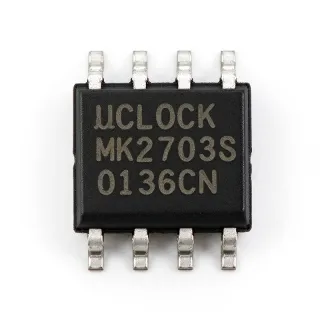
ICS409MLF - 80MHz LVCMOS PLL Clock Synthesizer | Renesas
MPN: ICS409MLF ✓ ActiveICS409MLF Overview
A clock synthesizer is a timing IC that converts a lower-frequency reference into one or more system clock signals. Clock synthesizer, PLL clock generator, and frequency multiplier are related terms within the clock and timing IC hierarchy, which also includes clock buffers, dividers, oscillators, and timer ICs. The ICS409MLF is intended to reduce the number of discrete components required in personal-computer peripheral applications.
The ICS409MLF supports a common 14.31818 MHz crystal through its on-chip crystal oscillator. Its PLL-based architecture multiplies the reference clock by three, producing an 80 MHz maximum output. The specified operating supply range is 3 V to 3.6 V, making the device suitable for systems using a 3.3 V clock domain.
The principal technical benefit is integration: a crystal oscillator, phase-locked loop, and frequency-multiplying output are combined in one IC. This reduces the component count compared with discrete oscillator and multiplier arrangements. The single-circuit implementation also simplifies clock routing, although output drive, jitter, phase accuracy, and loop stability must still be evaluated against the timing requirements of the target peripheral.
Typical applications include PC peripheral interfaces, legacy storage and bus controllers, embedded PC-compatible systems, and communication equipment requiring a 3.3 V LVCMOS reference clock. A 14.31818 MHz crystal is normally connected at the reference input, while the divided PLL architecture generates the higher-frequency clock used by the peripheral subsystem.
When laying out the circuit, keep the crystal and load capacitors close to the device and route the clock output away from noisy switching nodes. Confirm ground-plane continuity, output-load assumptions, and the required clock frequency before releasing the layout. Pin assignments and crystal-load details should be taken directly from the manufacturer pin-description table and application guidance.
Drop-in alternatives for ICS409MLF — same package, pin-to-pin compatible. Different-package parts requiring PCB rework are excluded.
Variants in this series
Same-series models that are drop-in compatible with ICS409MLF (same form factor and footprint) — differing in Package.
ICS409M
✅ Drop-InContact for price
View Datasheet →ICS409MLF Specifications
| Device Type | Clock/Frequency Synthesizer |
| PLL | Yes |
| Reference Input | 14.31818 MHz crystal |
| Output Logic | LVCMOS |
| Maximum Output Frequency | 80 MHz |
| Number of Circuits | 1 |
| Input-to-Output Frequency Ratio | 1:3 |
| Supply Voltage Range | 3 V to 3.6 V |
| Package | 8-SOIC |
| Mounting Type | Surface Mount |
| On-Chip Crystal Oscillator | Yes |
ICS409MLF 8-soic Pin Configuration Guide
Pin configuration for ICS409MLF (8-soic package). Pin numbering, functions, and connection diagrams are defined in the manufacturer datasheet. Refer to it for the exact footprint and soldering guidelines.

No detailed pinout data available for ICS409MLF.
Refer to the datasheet for full pin configuration.
Typical Applications
ICS409MLF is suitable for 6 applications: PC Peripheral Interface Clocking, Storage Controller Timing, Embedded PC-Compatible Systems, Industrial Communication Equipment, Instrumentation and Test Equipment, Legacy Bus and Interface Timing.
PC Peripheral Interface Clocking
The ICS409MLF fits legacy and embedded PC peripheral interfaces that require a stable 80 MHz clock in a 3.3 V domain. Its 14.31818 MHz crystal input and 1:3 frequency relationship let the on-chip PLL generate the required output without a separate frequency multiplier. The 8-SOIC package limits board area, while LVCMOS output suits conventional CMOS loads. Validate edge rate, jitter, and PLL startup in the complete interface timing environment.
Recommended
Storage Controller Timing
The ICS409MLF can provide the 80 MHz peripheral timing reference used by storage-controller and bus-interface sections of PC-compatible systems. Its integrated crystal oscillator and PLL reduce the component count compared with separate oscillator and multiplier stages. The 3 V to 3.6 V supply range aligns with 3.3 V controller logic, and the LVCMOS output simplifies interfacing. Designers should still check recovery time, clock duty-cycle limits, and output loading against the storage controller requirements.
Recommended
Embedded PC-Compatible Systems
The ICS409MLF is useful in embedded systems that retain PC peripheral timing but require a compact clock implementation. A 14.31818 MHz crystal provides the reference, and the PLL produces the documented 1:3 ratio for an 80 MHz maximum output. Because the clock generator is only 8 pins, it simplifies routing in space-constrained industrial or communications equipment. Confirm the required temperature grade and test the reference oscillator across the intended voltage and temperature range.
Recommended
Industrial Communication Equipment
The ICS409MLF can serve as a local timing source within industrial communication equipment that uses a PC-compatible clock domain. Its single PLL circuit, 3.3 V supply range, and compact 8-SOIC package support designs requiring deterministic integration with limited board space. The LVCMOS clock can feed compatible counters, communication controllers, or timing dividers. Use short clock traces, maintain a continuous ground reference, and validate jitter against the communication protocol's timing budget.
Recommended
Instrumentation and Test Equipment
The ICS409MLF can provide a compact 80 MHz reference clock for instrumentation subsystems that divide or gate the output into lower-rate timing domains. The integrated oscillator and PLL reduce assembly complexity, while LVCMOS output supports ordinary CMOS routing. For measurement equipment, place the crystal close to the device, provide a low-noise supply, and avoid routing the clock through switch-node neighborhoods. Confirm output jitter and frequency accuracy before using it as a precision reference.
Recommended
Legacy Bus and Interface Timing
The ICS409MLF is appropriate for legacy bus and peripheral-controller designs that expect an 80 MHz clock derived from a 14.31818 MHz reference. The 1:3 PLL relationship provides a straightforward way to generate the clock from a common crystal source, and the 3.3 V operation supports mixed legacy system architectures. The design must confirm that the 8-SOIC controller accepts the required clock amplitude and edge quality. Add source termination only if measurement shows excessive ringing.
Recommended
Recommended Products Summary
Engineering reference data for ICS409MLF — comparison, design guidance, and compliance information.
Selection Guide
Comparison with Alternatives
| Parameter | This Product | ICS409M |
|---|---|---|
| Brand | Renesas Electronics | Renesas Electronics |
| Package | 8-SOIC | 8-SOIC |
| Device Type | Clock/Frequency Synthesizer | Clock/Frequency Synthesizer |
| PLL | Yes | Yes |
| Reference Input | 14.31818 MHz crystal | 14.31818 MHz crystal |
| Output Logic | LVCMOS | LVCMOS |
| Maximum Output Frequency | 80 MHz | 80 MHz |
| Supply Voltage Range | 3 V to 3.6 V | 3 V to 3.6 V |
| Input-to-Output Ratio | 1:3 | 1:3 |
| Number of Circuits | 1 | 1 |
Key Differentiators
- Integrated reference oscillator and 3:1 multiplier (vs ICS409M)
- Compact 8-SOIC implementation (vs ICS409M)
- Defined 3.3 V operating domain (vs ICS409M)
Design Notes
Place the 14.31818 MHz crystal and its load capacitors directly beside the crystal-input pins. Keep the crystal loop compact, remove unnecessary copper beneath the crystal footprint where the layout guidance permits, and provide a continuous ground plane. Long crystal traces increase parasitic capacitance and pickup, which can reduce startup reliability or disturb frequency stability.
Route the 80 MHz LVCMOS clock as a short, controlled-impedance trace to the receiving circuit and keep it away from switching nodes and high-current return paths. Confirm output rise and fall time, duty-cycle distortion, ringing, and the receiver's allowable capacitance. A source-series termination resistor may be added if edge measurements reveal excessive overshoot, but it should not be populated without checking the clock amplitude at the load.
Do not substitute the 14.31818 MHz reference with an arbitrary oscillator without checking the PLL ratio and output frequency. The specified architecture accepts a 14.31818 MHz crystal and provides a 1:3 relationship, yielding up to 80 MHz. Also verify the exact pin names from the manufacturer datasheet because an eight-pin package does not, by itself, establish the power, ground, crystal, and clock-output assignments.
Operate the device only within its specified 3 V to 3.6 V supply range. Place the supply-decoupling capacitor close to the corresponding power pin and provide a low-impedance return path to the ground reference. Clock-generation circuits can exhibit startup or lock disturbances when the supply is noisy, so separate the reference oscillator from aggressive switching-regulator layouts where board partitioning permits.
Compliance Information
No definitive RoHS, REACH, AEC-Q100, lead-free, halogen-free, or conflict-minerals declarations were present in the product information for the ICS409MLF. Confirm compliance and automotive qualification using the current manufacturer product documentation before procurement.