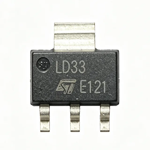
LD1117S33TR - 800mA Low Dropout Positive Regulator | STMicroelectronics
MPN: LD1117S33TR ✓ Active| Qty | Unit Price | Extended |
|---|---|---|
| 1 | $0.45 | $0.45 |
| 10 | $0.38 | $3.80 |
| 100 | $0.3 | $30.00 |
| 500 | $0.25 | $125.00 |
| 1,000 | $0.2 | $200.00 |
LD1117S33TR Overview
A low dropout regulator (LDO) is a type of linear voltage regulator that can maintain a stable output voltage even when the input voltage is very close to the output voltage, minimizing power dissipation. LDOs are essential in power management ICs, providing clean, low-noise supply rails for sensitive analog and digital circuits. The LD1117S33TR belongs to the LD1117 family, which includes adjustable and fixed output versions, and is widely used in consumer, industrial, and automotive applications.
Key features of the LD1117S33TR include a fixed 3.3V output, 800mA output current capability, internal current limiting, and thermal shutdown protection. The device offers a typical dropout voltage of 1.1V at full load, ensuring efficient operation even with low input-to-output voltage margins. The SOT-223 package provides a compact footprint with a thermal pad for improved heat dissipation, making it suitable for space-constrained designs.
The LD1117S33TR utilizes a PNP pass transistor architecture, which allows for low dropout operation and stable performance across a wide range of load currents. The internal current limiting and thermal shutdown features protect the device and the load from fault conditions. The device is stable with low ESR ceramic capacitors, simplifying the external component count and reducing board space.
Typical applications include post-regulation for switching power supplies, battery-powered equipment, and as a local supply rail for microcontrollers, FPGAs, and analog circuits. The fixed 3.3V output is ideal for powering 3.3V logic and mixed-signal systems. The wide input voltage range and robust protection features make it suitable for industrial control systems and consumer electronics.
When designing with the LD1117S33TR, ensure adequate input-to-output voltage headroom to maintain regulation under all load conditions. The dropout voltage increases with load current, so a minimum input voltage of 4.4V is recommended for a 3.3V output at 800mA. Proper PCB layout with adequate copper area for heat dissipation is essential for reliable operation at high load currents.
This page synthesizes distributor pricing, drop-in alternatives, and practical design notes not found in the STMicroelectronics datasheet, providing engineers with a comprehensive resource for selecting and implementing the LD1117S33TR.
Drop-in alternatives for LD1117S33TR — same package, pin-to-pin compatible. Different-package parts requiring PCB rework are excluded.
Variants in this series
Same-series models that are drop-in compatible with LD1117S33TR (same form factor and footprint) — differing in Line Regulation, Load Regulation, Output Voltage, Input Voltage Range, Quiescent Current.
Quick Comparison Tool — Select alternative parts for side-by-side comparison:
AMS1117-3.3
✅ Drop-In📋 Reference alternative (not in catalog)
NCP1117ST33T3G
✅ Drop-In📋 Reference alternative (not in catalog)
AP1117E33L-13
✅ Drop-In📋 Reference alternative (not in catalog)
LD1117S33TR Maximum Ratings & Electrical Characteristics
| Output Type | Fixed |
| Output Voltage | 3.3 V |
| Maximum Output Current | 800 mA |
| Input Voltage Range | Up to 15 V |
| Dropout Voltage | 1.1 V typical at 800 mA |
| Line Regulation | 0.2 % typical |
| Load Regulation | 0.4 % typical |
| Quiescent Current | 5 mA typical |
| Operating Temperature Range | 0°C to +125°C |
| Package | SOT-223 |
| Mounting Type | Surface Mount |
| MSL Level | 1 (unlimited) |
| RoHS Status | Compliant |
| REACH Status | Compliant |
| Thermal Resistance (junction-to-ambient) | 50 °C/W typical |
LD1117S33TR Pin Configuration
| Pin 1 | GND — Ground |
| Pin 2 | VOUT — Regulated 3.3V output |
| Pin 3 | VIN — Input voltage |
| Pin Tab | VOUT — Connected to output |
Typical Applications
LD1117S33TR is suitable for 6 applications: Post-Regulation for Switching Power Supplies, Battery-Powered Equipment, Industrial Control Systems, Consumer Electronics, FPGA and CPLD Power Supply, Automotive Electronics.
Post-Regulation for Switching Power Supplies
The LD1117S33TR is commonly used as a post-regulator after a switching converter to provide a clean, low-noise 3.3V rail. Its low dropout voltage allows efficient operation from a 5V intermediate bus, and its 800mA output current is sufficient for many digital loads. The device's internal current limiting and thermal shutdown protect the downstream circuitry. In this application, the LD1117S33TR is placed between the switching regulator output and the load, with input and output capacitors for stability. The low output noise and good line/load regulation ensure stable performance for sensitive components. Designers should consider the power dissipation across the LDO, as the dropout voltage multiplied by load current results in heat that must be managed via PCB copper area.
Recommended
Battery-Powered Equipment
In battery-powered devices, the LD1117S33TR regulates the battery voltage down to a stable 3.3V for logic circuits. Its low dropout voltage (1.1V at 800mA) allows the battery to discharge deeply before the regulator drops out, maximizing usable battery capacity. The low quiescent current of 5mA helps extend battery life in standby modes. The SOT-223 package is compact, making it suitable for portable devices. Designers should ensure the input voltage remains above the dropout threshold to maintain regulation. The device's thermal shutdown protects against overheating during high current draws. This application benefits from the LD1117S33TR's simplicity and reliability.
Recommended
Industrial Control Systems
The LD1117S33TR provides a stable 3.3V supply for microcontrollers, sensors, and communication interfaces in industrial control systems. Its wide input voltage range (up to 15V) allows it to be powered from 12V or 24V industrial buses with appropriate headroom. The device's robust protection features, including current limiting and thermal shutdown, ensure reliable operation in harsh environments. The SOT-223 package is suitable for PCB assembly in high-volume production. In this application, the LD1117S33TR is often used to power logic-level converters, CAN transceivers, and industrial sensors. Designers should consider the thermal dissipation when operating from higher input voltages, as the power loss is (VIN - VOUT) * ILOAD.
Recommended
Consumer Electronics
In consumer electronics such as set-top boxes, routers, and smart home devices, the LD1117S33TR provides a clean 3.3V rail for digital ICs. Its low cost and small footprint make it ideal for high-volume production. The device's fixed output simplifies design, and its stability with ceramic capacitors reduces BOM cost. The LD1117S33TR can be used to power Wi-Fi modules, audio codecs, and microcontrollers. Designers should ensure proper decoupling with 10uF input and output capacitors for stable operation. The device's thermal shutdown protects against fault conditions, enhancing product reliability.
Recommended
FPGA and CPLD Power Supply
The LD1117S33TR can power the auxiliary 3.3V rail of FPGAs and CPLDs, which often require a clean supply for I/O banks and configuration logic. Its 800mA output current is sufficient for many small to medium FPGAs. The low dropout voltage ensures efficient operation from a 5V input. The device's low output noise helps maintain signal integrity. In this application, the LD1117S33TR is typically used in conjunction with core voltage regulators. Designers should place the LDO close to the FPGA to minimize trace inductance and ensure stable voltage at the load. The thermal pad of the SOT-223 package should be connected to a copper pour for heat dissipation.
Recommended
Automotive Electronics
The LD1117S33TR is used in automotive electronics for powering sensors, microcontrollers, and communication interfaces that require a stable 3.3V supply. Its wide input voltage range accommodates automotive battery voltage variations (9V to 16V). The device's thermal shutdown and current limiting provide protection in harsh automotive environments. The SOT-223 package is suitable for engine control units and body control modules. In this application, the LD1117S33TR is often powered from a 5V rail generated by a switching regulator. Designers should ensure the input voltage does not exceed the absolute maximum rating of 15V, and consider adding a transient voltage suppressor for load dump protection.
Recommended
Recommended Products Summary
Engineering reference data for LD1117S33TR — comparison, design guidance, and compliance information.
Selection Guide
Comparison with Alternatives
| Parameter | This Product | AMS1117-3.3 | NCP1117ST33T3G | AP1117E33L-13 |
|---|---|---|---|---|
| Package | SOT-223 | SOT-223 | SOT-223 | SOT-223 |
| Output Voltage | 3.3V | 3.3V | 3.3V | 3.3V |
| Maximum Output Current | 800mA | 800mA | 1A | 1A |
| Dropout Voltage (typical) | 1.1V at 800mA | 1.1V at 800mA | 1.1V at 800mA | 1.1V at 800mA |
| Input Voltage Range | Up to 15V | Up to 15V | Up to 20V | Up to 18V |
| Quiescent Current | 5mA typical | 5mA typical | 5mA typical | 5mA typical |
| Operating Temperature Range | 0°C to +125°C | 0°C to +125°C | -40°C to +125°C | -40°C to +125°C |
| RoHS Compliant | Yes | Yes | Yes | Yes |
Key Differentiators
- STMicroelectronics quality and reliability (vs AMS1117-3.3)
- Wide input voltage range up to 15V (vs NCP1117ST33T3G)
- Pin-to-pin compatible with common alternatives (vs AP1117E33L-13)
Design Notes
The LD1117S33TR in SOT-223 has a typical junction-to-ambient thermal resistance of 50°C/W. For a 12V input to 3.3V output at 800mA, power dissipation is (12-3.3)*0.8 = 6.96W, which would cause a temperature rise of 348°C, far exceeding the maximum junction temperature. Therefore, such high input voltages are not practical at full load. For reliable operation, keep power dissipation below 1W, which requires a maximum input voltage of 4.55V at 800mA. Use adequate PCB copper area and consider a heatsink or thermal vias for higher dissipation.
Place input and output capacitors as close to the IC pins as possible. Use a 10uF ceramic capacitor on the input and a 10uF ceramic capacitor on the output. Add a 0.1uF ceramic capacitor in parallel for high-frequency noise bypass. The SOT-223 tab is connected to VOUT and should be soldered to a large copper pad for heat dissipation.
Do not exceed the maximum input voltage of 15V. Ensure the input voltage is at least 4.4V for a 3.3V output at 800mA to maintain regulation. The device is stable with low ESR ceramic capacitors, but avoid using capacitors with ESR below 0.5 ohm if the device is not designed for it. Always check the absolute maximum ratings and derate for temperature.
Compliance Information
RoHS and REACH compliant per STMicroelectronics product page. Not AEC-Q100 qualified; for automotive, consider AEC-qualified alternatives.
