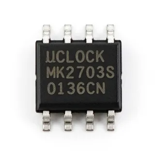
MK2304S-1ILFT - 133MHz Zero Delay Buffer | Renesas
MPN: MK2304S-1ILFT ✓ ActiveMK2304S-1ILFT Overview
A zero-delay buffer is a clock-management integrated circuit that compensates for the propagation delay introduced by clock routing. It belongs to the clock buffer family within clock and timing ICs, where buffer, driver, and PLL-based devices distribute high-speed reference clocks across a system. The MK2304S-1ILFT combines one clock circuit, a clock input, CMOS outputs, and PLL capability in a surface-mount package.
The device supports operation to 133 MHz and is identified as a low-skew zero-delay buffer. These characteristics are significant in systems where multiple loads must receive closely related clock transitions. The 8-SOIC package provides a compact surface-mount solution for PCB designs that require more than a passive delay element but do not need the functional complexity of a general-purpose clock generator.
In the digital signal path, the buffer accepts a clock signal and provides a corresponding CMOS clock output. Its zero-delay architecture is intended to preserve system timing relationships more effectively than ordinary logic-buffer routing, where cumulative gate and trace delay can shift clock arrival times. PLL capability provides an additional clock-related function, although operating mode, feedback topology, and configuration details must be established from the manufacturer datasheet.
Typical applications include clock distribution for communications equipment, processor and memory clock interfaces, embedded control systems, industrial automation, and consumer electronics. The 133 MHz maximum operating frequency makes the device relevant to legacy and established digital platforms rather than the highest-speed contemporary processor interfaces. The 3.90 mm-wide SOIC package also supports conventional surface-mount assembly and repair workflows.
PCB implementation should preserve a short, symmetric clock path between the source, buffer, and receiving circuits. Place the device close to the clock source or load it is intended to buffer, use a continuous ground reference, and avoid routing the clock through test pads or long parallel segments where avoidable. Decoupling capacitors should be positioned close to the supply and ground pins according to the manufacturer’s reference layout.
This product page combines the manufacturer device description with application guidance, design considerations, and a structured comparison framework. It supports engineers evaluating the MK2304S-1ILFT for low-skew clock distribution, replacement planning, footprint verification, and PCB implementation in 8-SOIC designs.
Drop-in alternatives for MK2304S-1ILFT — same package, pin-to-pin compatible. Different-package parts requiring PCB rework are excluded.
No drop-in alternatives available for this product.
Request AlternativesMK2304S-1ILFT Specifications
| Device Type | Zero Delay Buffer |
| Description | Zero Delay, Low Skew Buffer |
| Maximum Operating Frequency | 133 MHz |
| Number of Circuits | 1 circuit |
| PLL | Yes |
| Input Type | Clock |
| Output Type | CMOS |
| Package | 8-SOIC |
| Package Width | 3.90 mm |
| Package Length | 0.154 inch |
| Mounting Type | Surface Mount |
MK2304S-1ILFT 0.154 inch Pin Configuration Guide
Pin configuration for MK2304S-1ILFT (0.154 inch package). Pin numbering, functions, and connection diagrams are defined in the manufacturer datasheet. Refer to it for the exact footprint and soldering guidelines.

No detailed pinout data available for MK2304S-1ILFT.
Refer to the datasheet for full pin configuration.
Typical Applications
MK2304S-1ILFT is suitable for 6 applications: Embedded Control Clock Distribution, Processor and Memory Interface Clocks, Communications Equipment Clocking, Industrial Automation Control, Consumer and Embedded Electronics, Test and Measurement Instrumentation.
Embedded Control Clock Distribution
The Renesas Electronics MK2304S-1ILFT fits embedded-control designs that require a buffered clock to reach multiple digital logic sections. Its 133 MHz maximum operating frequency covers established controller and peripheral clock domains, while the zero-delay, low-skew architecture helps preserve relative clock arrival times across PCB traces. The CMOS output suits modern digital logic, and the one-circuit configuration makes the device appropriate when a single source clock needs buffering rather than multiplication. Because the package is an 8-SOIC, the part also fits conventional surface-mount PCB assembly. Verify supply voltage, output configuration, and all eight physical pin positions against the manufacturer datasheet before placing it beside an embedded processor or controller.
Processor and Memory Interface Clocks
The MK2304S-1ILFT is applicable to processor, memory, and peripheral clock routing where clock timing must remain consistent between source and load. Its 133 MHz ceiling makes it suitable for established data buses and control logic operating below that frequency, and its zero-delay function is intended to compensate for routing delay encountered between the clock source and receiving circuits. Low-skew operation is valuable when multiple destinations depend on the same reference edge. The CMOS output provides a direct fit for common digital clock signaling, while the active buffering role can isolate the source from load-dependent trace effects. Confirm interface timing, loading, voltage levels, and PLL configuration in the manufacturer documentation before replacing a passive or gate-based clock distribution arrangement.
Communications Equipment Clocking
The MK2304S-1ILFT can support clock distribution in communications equipment built around established digital logic below 133 MHz. A communications subsystem may require the reference clock to reach a transceiver, controller, or memory subsystem with tightly controlled timing, and the device’s zero-delay, low-skew buffer function is intended to reduce the effect of routing delay. Its CMOS output and PLL capability make it relevant where the clock path must be regenerated or conditioned rather than split passively. The 8-SOIC package permits routing away from connector and processor footprints that would be difficult to service. Confirm input amplitude, output loading, supply range, and bypass requirements with the Renesas manufacturer datasheet before finalizing the clock tree.
Industrial Automation Control
The MK2304S-1ILFT is suitable for industrial automation control boards that distribute a common clock to logic, measurement, and interface subsystems. The 133 MHz maximum frequency covers many conventional control and data-acquisition architectures, while low-skew buffering helps prevent clock arrival differences from creating inconsistent capture windows. CMOS output supports common digital logic, and PLL capability may be useful in more complex clock trees. Its compact 8-SOIC footprint is practical for densely populated control boards and simplifies replacement with a conventional surface-mount assembly process. Design the layout with short clock traces, a continuous ground plane, and local supply bypassing. Confirm electrical limits and environmental requirements directly from the manufacturer documentation for the deployed industrial system.
Consumer and Embedded Electronics
The MK2304S-1ILFT can serve as a clock-distribution element in consumer and embedded electronic products built around legacy or mid-speed digital logic. The device provides a 133 MHz zero-delay, low-skew CMOS output from a clock input, allowing a system designer to distribute a reference clock without relying on the limited drive strength of an ordinary logic gate. Its one-circuit arrangement suits a single buffered clock path, and the 8-SOIC package offers broad compatibility with established PCB assembly methods. Consumers of older embedded platforms should still validate signal levels, timing margins, and PLL mode before using the device in a new design. Placement close to the clock consumer, short supply connections, and proper decoupling are essential for predictable behavior.
Test and Measurement Instrumentation
The MK2304S-1ILFT is relevant to test and measurement instrumentation that clocks acquisition, processing, or interface logic at rates up to 133 MHz. Its zero-delay, low-skew operation can help maintain controlled relative timing between a buffered clock source and downstream circuits, while CMOS outputs match common digital acquisition and control components. The one-circuit configuration is appropriate where a single conditional or unconditioned reference clock must be regenerated for a sensitive load. The 8-SOIC package is easy to incorporate on instrument-control and high-speed digital daughtercards. Designers should minimize trace length, keep the clock path away from noisy switching nodes, and validate output loading and jitter performance against the complete instrumentation timing budget.
Engineering reference data for MK2304S-1ILFT — comparison, design guidance, and compliance information.
Selection Guide
Comparison with Alternatives
| Parameter | This Product |
|---|---|
| Device Type | Zero Delay, Low Skew Buffer |
| Maximum Frequency | 133 MHz |
| Number of Circuits | 1 circuit |
| Input Type | Clock |
| Output Type | CMOS |
| PLL Capability | Yes |
| Package | 8-SOIC |
| Brand | Renesas Electronics |
Key Differentiators
- Purpose-built zero-delay clock buffering (vs Conventional CMOS logic buffer)
- Integrated PLL capability (vs Passive clock-delay element)
- Single-circuit CMOS implementation (vs Multi-output clock distributor)
Design Notes
Place the MK2304S-1ILFT close to the clock source or the load requiring regeneration, and route the clock through a short, continuous path. Avoid inserting long traces, unnecessary vias, test pads, or parallel runs beside noisy switching signals. The 8-SOIC footprint provides a conventional surface-mount assembly option, but placement quality remains important for maintaining the low-skew behavior expected from a zero-delay clock buffer.
Treat the clock connection as a controlled-impedance signal path rather than a general logic net. Maintain a continuous reference plane, use short return paths, and keep the device away from switching regulators, inductors, and high-current power paths. Confirm output loading and the complete clock topology in the Renesas manufacturer datasheet because propagation delay, skew, and usable loading determine whether the buffered clock meets the receiving circuit’s timing requirement.
Do not assume that a zero-delay buffer has zero propagation delay; the function is intended to compensate routing delay while introducing its own device timing. Likewise, do not substitute a conventional CMOS inverter or generic clock driver solely because its frequency rating appears similar. Verify all eight 8-SOIC pin functions, supply requirements, output configuration, and PLL mode against the manufacturer datasheet before releasing the PCB design.
Compliance Information
Compliance status must be confirmed from the manufacturer documentation for the ordered device and manufacturing lot.