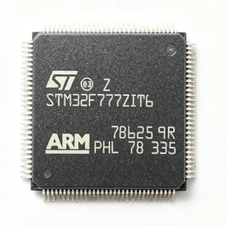
MMC2114CFCAG33 - 32-bit M210 MCU 256KB Flash | NXP
MPN: MMC2114CFCAG33 ✗ End of Life| Qty | Unit Price | Extended |
|---|---|---|
| 1 | $24.5 | $24.50 |
| 10 | $22.8 | $228.00 |
| 100 | $20.4 | $2,040.00 |
| 500 | $18.6 | $9,300.00 |
| 1,000 | $17.2 | $17,200.00 |
MMC2114CFCAG33 Overview
A 32-bit microcontroller (MCU) integrates a processor core, memory, and digital and analog peripherals on a single chip, sitting within the broader hierarchy of embedded processors: MCU -> microcontroller unit -> embedded processor -> semiconductor IC. Single-chip microcontrollers like the MMC2114 reduce system cost and board space compared to multi-chip CPU-plus-memory designs.
The MMC2114 is the second member of the M210-based general-purpose family and cost-effectively integrates digital and analog peripherals with RAM and embedded FLASH on a single die. According to NXP, the MMC2114 expands on the popular MMC2107 with twice the FLASH memory and four times the SRAM, making it a direct upgrade path for existing MMC2107 designs without board redesign, since both share the same 144-pin LQFP footprint.
The M-CORE architecture is a 16/32-bit microRISC design optimized for high code density and low power consumption at modest clock rates. At 33 MHz, the core delivers predictable real-time performance suitable for control-oriented embedded tasks. The 3.3 V supply rail matches standard logic levels used across industrial and automotive-adjacent systems.
Typical applications include industrial control systems, motor control and actuation, instrumentation, automotive body and convenience modules, and legacy embedded systems requiring long-term spare availability. The integrated FLASH enables in-field firmware updates without external program memory.
Designers should note that NXP has declared this device End of Life; new designs should evaluate current-generation NXP MCUs, while maintenance designs should secure last-time-buy stock through authorized excess-inventory distributors such as Rochester Electronics.
This page synthesizes distributor pricing, drop-in family alternatives, lifecycle status, and practical design guidance not consolidated in the manufacturer datasheet, providing a single reference for engineers supporting MMC2114-based systems.
Drop-in alternatives for MMC2114CFCAG33 — same package, pin-to-pin compatible. Different-package parts requiring PCB rework are excluded.
Variants in this series
Same-series models that are drop-in compatible with MMC2114CFCAG33 (same form factor and footprint) — differing in Program Memory Size, Core Architecture, Core Processor, Package, RAM Size.
Quick Comparison Tool — Select alternative parts for side-by-side comparison:
MMC2107CFCAG33
✅ Drop-In✓ In Stock
$8.2 / Unit
View Datasheet →MMC2114CFCAG33
✅ Drop-In✓ In Stock
$17.2 / Unit
View Datasheet →MMC2114CFCAG33 Maximum Ratings & Electrical Characteristics
| Core Processor | M210 (M-CORE microRISC) |
| Core Architecture | 16/32-bit |
| Maximum Clock Frequency | 33 MHz |
| Program Memory Size | 256 KB (256K x 8) FLASH |
| RAM Size | 32 KB |
| Data Bus Width | 32 bit |
| Supply Voltage | 3.3 V |
| Product Series | MMC2114 (M210) |
| Package Type | LQFP-144 (20x20 mm) |
| Number of Terminals | 144 |
| Terminal Form | Gull Wing |
| Terminal Finish | Tin |
| Mounting Type | Surface Mount |
| Package Shape | Square |
| Product Category | Microcontrollers (MCU) |
MMC2114CFCAG33 square Pin Configuration Guide
Pin configuration for MMC2114CFCAG33 (square package). This digital IC includes GPIO, communication interfaces (UART, SPI, I2C), and power pins. Refer to the manufacturer datasheet for alternate pin functions and configuration options. Essential for embedded system design and PCB layout.

No detailed pinout data available for MMC2114CFCAG33.
Refer to the datasheet for full pin configuration.
Typical Applications
MMC2114CFCAG33 is suitable for 6 applications: Industrial Control Systems, Instrumentation and Test Equipment, Automotive Body and Convenience Modules, Motor Control and Actuation, Legacy Embedded System Maintenance, Communication and Protocol Interface Nodes.
Industrial Control Systems
The MMC2114CFCAG33 fits industrial control nodes that require deterministic, control-oriented processing at modest clock rates. Its 32-bit M210 microRISC core at 33 MHz delivers predictable real-time execution for loop control and sequencing tasks, while the 256 KB embedded FLASH accommodates protocol stacks and application code without external program memory, and the 32 KB SRAM supports control state machines and communication buffers. In a typical design, the MCU runs the main control loop from internal FLASH at 3.3 V, using its integrated digital and analog peripherals to interface sensors, actuators, and supervisory circuits directly, reducing external component count and board area. The trade-off versus a modern MCU is lower peripheral integration and EOL status, so it is best deployed as a form-fit-function replacement in existing industrial boards rather than new designs, with stock secured through authorized aftermarket channels before inventory depletes.
Recommended
Instrumentation and Test Equipment
For bench and panel instrumentation, the MMC2114CFCAG33 provides sufficient on-chip memory and I/O to manage front-panel interfaces, measurement sequencing, and result formatting from a single chip. The 256 KB FLASH stores lookup tables and firmware for measurement algorithms, while 32 KB SRAM buffers acquired data before transmission over communication interfaces. Its 3.3 V supply and LQFP-144 pin count give designers abundant general-purpose I/O for keypad scanning, display driving, and peripheral control in a 20x20 mm footprint that fits standard instrument main boards. Because the M210 core consumes little power at 33 MHz, thermal design is straightforward in enclosed instruments. As the device is EOL, instrument manufacturers typically use it for sustaining engineering of shipped products, pairing it with stock purchased during the last-time-buy window or from Rochester Electronics authorized aftermarket production.
Recommended
Automotive Body and Convenience Modules
The M210 family was historically deployed in control modules such as body electronics and convenience functions, where moderate performance, low power, and single-chip integration are valued. The MMC2114CFCAG33's integrated digital and analog peripherals allow direct driving of loads and reading of switches and sensors without a coprocessor, while the embedded FLASH supports field firmware updates for feature changes during the vehicle program. Its 3.3 V operation aligns with standard module logic rails derived from the 12 V battery via a switching regulator. However, this part carries no current AEC-Q100 qualification claim in the available data and is EOL, so it is appropriate only for service parts and legacy module continuity. For new automotive modules, NXP's SPC5 family (e.g., SPC5602BF2MLL6, SPC5644AF0MLU2) provides actively produced, automotive-qualified successors.
Recommended
Motor Control and Actuation
Control-oriented actuation systems - such as position servos, valve controllers, and small motor drives - benefit from the MMC2114CFCAG33's deterministic microRISC core, whose instruction set executes control loops efficiently at 33 MHz without pipelining complexity. The 32 KB SRAM retains loop state, trajectory tables, and communication frames, while 256 KB FLASH holds parameter sets for multiple actuator variants, allowing one PCB to serve a product family. The wide peripheral set of the M210 single-chip design interfaces PWM outputs and feedback inputs directly. Power stages are external, typically driven through gate drivers, since the MCU operates at 3.3 V logic levels. The main engineering consideration is EOL risk: actuation platforms often remain in production for decades, so designers sustaining such platforms should map a migration path to NXP's actively produced MCUs and hold safety stock of the MMC2114.
Recommended
Legacy Embedded System Maintenance
The primary ongoing use of the MMC2114CFCAG33 is sustaining engineering for shipped embedded systems whose firmware is written for the M210 M-CORE architecture. Because the MMC2114 shares its 144-pin LQFP footprint and peripheral map with the MMC2107, boards designed around the family can swap memory-grade variants with minimal PCB changes, and the MMC2114's doubled FLASH (256 KB) and quadrupled SRAM (32 KB) absorb firmware growth accumulated over product lifetime. Sourcing is the critical activity: with NXP declaring the device End of Life, maintenance programs should register last-time-buy quantities with franchised distributors and qualify Rochester Electronics authorized aftermarket production as the continuity source. Firmware teams should also freeze toolchains and keep programming adapters, since M-CORE development environments are no longer actively supported.
Recommended
Communication and Protocol Interface Nodes
Embedded communication nodes - gateways, protocol converters, and remote I/O heads - use the MMC2114CFCAG33's single-chip integration to terminate serial links, buffer traffic in the 32 KB SRAM, and execute protocol stacks from the 256 KB FLASH. The M210 core's code density allows full stack implementations in the on-chip memory without external storage, improving reliability in electrically noisy environments, and the 3.3 V I/O levels interface standard transceivers directly. The 144-pin LQFP provides enough I/O for multiple simultaneous channels and status indications. Designers should budget the 33 MHz core carefully for bandwidth-heavy protocols, since this is modest by modern standards. Given the EOL status, this application is limited to existing product lines; new node designs should select current NXP devices such as the S912XET512BMAGR (S12X family) which combine active production with automotive-grade pedigree.
Recommended
Recommended Products Summary
Engineering reference data for MMC2114CFCAG33 — comparison, design guidance, and compliance information.
Selection Guide
Comparison with Alternatives
| Parameter | This Product | MMC2107CFCAG33 | MMC2114CFCAG33 (Rochester) |
|---|---|---|---|
| Package | LQFP-144 (20x20 mm) | LQFP-144 (20x20 mm) - same | LQFP-144 (20x20 mm) - same |
| Brand | NXP Semiconductors (Freescale) | NXP Semiconductors (Freescale) | NXP Semiconductors via Rochester Electronics |
| Core | M210 M-CORE 16/32-bit | M210 M-CORE 16/32-bit | M210 M-CORE 16/32-bit |
| Max Clock Frequency | 33 MHz | 33 MHz | 33 MHz |
| FLASH Memory | 256 KB | 128 KB | 256 KB |
| SRAM | 32 KB | 8 KB | 32 KB |
| Lifecycle Status | EOL (NXP) | EOL | Available via authorized aftermarket |
| Supply Voltage | 3.3 V | 3.3 V | 3.3 V |
Key Differentiators
- Double the memory of the base-family part (vs MMC2107CFCAG33)
- Authorized aftermarket continuity available (vs MMC2107CFCAG33 (franchised stock only))
- Single-chip integration (vs MMC2107CFCAG33)
Design Notes
The MMC2114CFCAG33 is End of Life per the NXP product page. Before committing any new or sustaining design, confirm stock availability and secure a last-time-buy. Qualify Rochester Electronics authorized aftermarket production as your continuity source, and consider designing a firmware-compatible migration path to an actively produced NXP family (ColdFire or S12X) to avoid future obsolescence risk in long-life products.
The device operates from a 3.3 V supply. Derive the 3.3 V rail from a 5 V or 12 V system rail using a switching regulator with adequate ripple filtering, and place 100 nF ceramic decoupling capacitors at multiple LQFP-144 supply pin pairs plus bulk capacitance near the package. Verify that all I/O connected to the MCU respects the 3.3 V logic level, since the M-CORE I/O is not 5 V tolerant unless the datasheet explicitly states so.
The 144-lead LQFP (20x20 mm, 0.5 mm pitch gull-wing leads) requires a fine-pitch SMD land pattern per the manufacturer package drawing. Use solder-mask-defined pads with ~10% oversize for inspection access, route the crystal and clock traces short and guarded by ground, and allocate thermal relief via ground planes tied to exposed GND pins. Follow the recommended footprint dimensions in the manufacturer datasheet package section rather than generic LQFP-144 patterns.
At 33 MHz, external bus operation should observe signal integrity basics: keep address/data bus traces under 100 mm where possible, match trace lengths on parallel bus groups to reduce skew, and add series termination (22-33 ohm) on fast edges to control ringing. Ensure a solid ground return plane beneath bus routing, and keep analog peripheral signals physically separated from switching clock traces within the 20x20 mm package fanout region.
Compliance Information
The official NXP product page lists an 'Environmental Quality' section for this part, but specific RoHS/REACH/lead-free status values were not included in the retrieved data. Terminal finish is documented as Tin (per Vyrian listing). Consult the NXP Environmental Quality page for the exact compliance declarations.