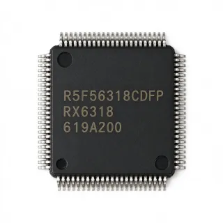
R5F52205BDFP#10 - 32MHz RX220 MCU 128KB Flash 100-LFQFP | Renesas
MPN: R5F52205BDFP#10 ✓ Active| Qty | Unit Price | Extended |
|---|---|---|
| 1 | $6.59 | $6.59 |
| 10 | $6.2 | $62.00 |
| 100 | $5.65 | $565.00 |
| 500 | $5.1 | $2,550.00 |
| 1,000 | $4.62 | $4,620.00 |
R5F52205BDFP#10 Overview
What is a microcontroller (MCU)? A microcontroller is a single-chip computer that integrates a CPU core, program memory (flash), data memory (SRAM), and peripherals such as timers, communication interfaces, and analog blocks. The RX220 family sits within the broader taxonomy: 32-bit MCU -> microcontroller -> embedded processor -> semiconductor IC. RXv1 cores use the Renesas RX instruction set, delivering high code density and deterministic interrupt response suited to real-time embedded designs.
Key features of the R5F52205BDFP#10 include 128KB flash with 8KB SRAM, a 32MHz maximum operating frequency, and an industrial temperature grade of -40C to +85C. The device integrates a minimum set of peripherals aimed at entry-level designs: multiple timers, a 12-bit A/D converter, and serial communication interfaces. The 100-pin LFQFP package provides ample I/O for typical embedded applications while remaining cost-effective for high-volume production.
The RX220 Group achieves high pin-arrangement and software compatibility with the higher-end RX210 Group, allowing engineers to migrate designs upward as memory or peripheral needs grow. This compatibility reduces design risk and accelerates time-to-market when scaling from entry-level to mid-range applications.
Typical applications include home appliances, consumer electronics, industrial sensor nodes, simple motor control, and battery-powered measurement instruments. The wide 1.62V-5.5V operating range supports both 3.3V and 5V system designs without external level translation.
When designing with this MCU, ensure the power supply rail stays within 1.62V-5.5V during all transient conditions, and follow Renesas RX220 hardware manual guidance for oscillator and reset circuit design. Unused pins should be configured with appropriate input pull-ups or left open per the hardware manual to minimize power consumption.
This page synthesizes distributor pricing from DigiKey, Mouser, and LCSC, drop-in alternatives from the RX220 family and cross-brand ARM Cortex-M0+ competitors, and practical design notes not consolidated in the manufacturer datasheet.
Drop-in alternatives for R5F52205BDFP#10 — same package, pin-to-pin compatible. Different-package parts requiring PCB rework are excluded.
Variants in this series
Same-series models that are drop-in compatible with R5F52205BDFP#10 (same form factor and footprint) — differing in Package, A/D Converter, Core Architecture, Operating Temperature, Program Memory (Flash).
Quick Comparison Tool — Select alternative parts for side-by-side comparison:
R5F52205BDFP#30
✅ Drop-In📋 Reference alternative (not in catalog)
R5F52206BDFP#10
✅ Drop-In📋 Reference alternative (not in catalog)
R5F52203BDFL
✅ Drop-In✓ In Stock
$2.62 / Unit
View Datasheet →R5F211B4SP#W4
✅ Drop-In✓ In Stock
$3.04 / Unit
View Datasheet →NUC029TAN
✅ Drop-In📋 Reference alternative (not in catalog)
GD32F130R8T6
✅ Drop-In📋 Reference alternative (not in catalog)
R5F52205BDFP#10 Maximum Ratings & Electrical Characteristics
| Product Series | RX220 Group |
| Core Architecture | RXv1 (32-bit) |
| Maximum Operating Frequency | 32 MHz |
| Program Memory (Flash) | 128 KB (128K x 8) |
| Data Memory (SRAM) | 8 KB |
| Supply Voltage Range | 1.62 V to 5.5 V |
| Operating Temperature Range | -40 C to +85 C |
| Package | 100-LFQFP (14x14 mm) |
| Mounting Type | Surface Mount |
| Pin Count | 100 |
| A/D Converter | 12-bit |
| RoHS Status | Compliant |
| Lead-Free | Yes |
| Peripheral Count | Minimum (entry-level positioning) |
R5F52205BDFP#10 Pin Configuration
| Pin 1 | VCL — Smooth-capacitor pin for internal voltage regulator (connect 0.1uF to VSS) |
| Pin 2 | VSS — Ground reference |
| Pin 3 | P50/IRQ0 — Port 5 / external interrupt request 0 |
| Pin 4 | P51/IRQ1 — Port 5 / external interrupt request 1 |
| Pin 5 | MD/FINEC — Mode select / fine clock input |
| Pin 6 | RES# — Reset input (active low) |
| Pin 7 | XTAL/PGEC — Crystal oscillator / programming clock |
| Pin 8 | EXTAL/PGED — External clock / programming data |
| Pin 9 | VSS — Ground reference |
| Pin 10 | AVSS0 — Analog ground for ADC0 |
| Pin 11 | AVCC0 — Analog supply for ADC0 |
| Pin 12 | P40/AN000 — Port 4 / ADC0 analog input 0 |
| Pin 13 | P41/AN001 — Port 4 / ADC0 analog input 1 |
| Pin 14 | P42/AN002 — Port 4 / ADC0 analog input 2 |
| Pin 15 | P43/AN003 — Port 4 / ADC0 analog input 3 |
| Pin 16 | P44/AN004 — Port 4 / ADC0 analog input 4 |
| Pin 17 | P45/AN005 — Port 4 / ADC0 analog input 5 |
| Pin 18 | P46/AN006 — Port 4 / ADC0 analog input 6 |
| Pin 19 | P47/AN007 — Port 4 / ADC0 analog input 7 |
| Pin 20 | VREFH0 — ADC0 high reference voltage |
| Pin 21 | VREFL0 — ADC0 low reference voltage |
| Pin 22 | AVSS0 — Analog ground for ADC0 |
| Pin 23 | P03 — Port 0 general-purpose I/O |
| Pin 24 | P02 — Port 0 general-purpose I/O |
| Pin 25 | P01 — Port 0 general-purpose I/O |
| Pin 26 | P00 — Port 0 general-purpose I/O |
| Pin 27 | P07 — Port 0 general-purpose I/O |
| Pin 28 | P06 — Port 0 general-purpose I/O |
| Pin 29 | P05 — Port 0 general-purpose I/O |
| Pin 30 | P04 — Port 0 general-purpose I/O |
| Pin 31 | P17 — Port 1 general-purpose I/O |
| Pin 32 | P16 — Port 1 general-purpose I/O |
| Pin 33 | P15 — Port 1 general-purpose I/O |
| Pin 34 | P14 — Port 1 general-purpose I/O |
| Pin 35 | P13 — Port 1 general-purpose I/O |
| Pin 36 | P12 — Port 1 general-purpose I/O |
| Pin 37 | P11 — Port 1 general-purpose I/O |
| Pin 38 | P10 — Port 1 general-purpose I/O |
| Pin 39 | P27 — Port 2 general-purpose I/O |
| Pin 40 | P26 — Port 2 general-purpose I/O |
| Pin 41 | P25 — Port 2 general-purpose I/O |
| Pin 42 | P24 — Port 2 general-purpose I/O |
| Pin 43 | P23 — Port 2 general-purpose I/O |
| Pin 44 | P22 — Port 2 general-purpose I/O |
| Pin 45 | P21 — Port 2 general-purpose I/O |
| Pin 46 | P20 — Port 2 general-purpose I/O |
| Pin 47 | P87 — Port 8 general-purpose I/O |
| Pin 48 | P86 — Port 8 general-purpose I/O |
| Pin 49 | P85 — Port 8 general-purpose I/O |
| Pin 50 | P84 — Port 8 general-purpose I/O |
| Pin 51 | P83 — Port 8 general-purpose I/O |
| Pin 52 | P82 — Port 8 general-purpose I/O |
| Pin 53 | P81 — Port 8 general-purpose I/O |
| Pin 54 | P80 — Port 8 general-purpose I/O |
| Pin 55 | P97 — Port 9 general-purpose I/O |
| Pin 56 | P96 — Port 9 general-purpose I/O |
| Pin 57 | P95 — Port 9 general-purpose I/O |
| Pin 58 | P94 — Port 9 general-purpose I/O |
| Pin 59 | P93 — Port 9 general-purpose I/O |
| Pin 60 | P92 — Port 9 general-purpose I/O |
| Pin 61 | P91 — Port 9 general-purpose I/O |
| Pin 62 | P90 — Port 9 general-purpose I/O |
| Pin 63 | PA7 — Port A general-purpose I/O |
| Pin 64 | PA6 — Port A general-purpose I/O |
| Pin 65 | PA5 — Port A general-purpose I/O |
| Pin 66 | PA4 — Port A general-purpose I/O |
| Pin 67 | PA3 — Port A general-purpose I/O |
| Pin 68 | PA2 — Port A general-purpose I/O |
| Pin 69 | PA1 — Port A general-purpose I/O |
| Pin 70 | PA0 — Port A general-purpose I/O |
| Pin 71 | PB7 — Port B general-purpose I/O |
| Pin 72 | PB6 — Port B general-purpose I/O |
| Pin 73 | PB5 — Port B general-purpose I/O |
| Pin 74 | PB4 — Port B general-purpose I/O |
| Pin 75 | PB3 — Port B general-purpose I/O |
| Pin 76 | PB2 — Port B general-purpose I/O |
| Pin 77 | PB1 — Port B general-purpose I/O |
| Pin 78 | PB0 — Port B general-purpose I/O |
| Pin 79 | PC7 — Port C general-purpose I/O |
| Pin 80 | PC6 — Port C general-purpose I/O |
| Pin 81 | PC5 — Port C general-purpose I/O |
| Pin 82 | PC4 — Port C general-purpose I/O |
| Pin 83 | PC3 — Port C general-purpose I/O |
| Pin 84 | PC2 — Port C general-purpose I/O |
| Pin 85 | PC1 — Port C general-purpose I/O |
| Pin 86 | PC0 — Port C general-purpose I/O |
| Pin 87 | PD7 — Port D general-purpose I/O |
| Pin 88 | PD6 — Port D general-purpose I/O |
| Pin 89 | PD5 — Port D general-purpose I/O |
| Pin 90 | PD4 — Port D general-purpose I/O |
| Pin 91 | PD3 — Port D general-purpose I/O |
| Pin 92 | PD2 — Port D general-purpose I/O |
| Pin 93 | PD1 — Port D general-purpose I/O |
| Pin 94 | PD0 — Port D general-purpose I/O |
| Pin 95 | PE7 — Port E general-purpose I/O |
| Pin 96 | PE6 — Port E general-purpose I/O |
| Pin 97 | PE5 — Port E general-purpose I/O |
| Pin 98 | PE4 — Port E general-purpose I/O |
| Pin 99 | PE3 — Port E general-purpose I/O |
| Pin 100 | VCC — Main digital supply input |
Typical Applications
R5F52205BDFP#10 is suitable for 6 applications: Home Appliance Control, Industrial Sensor Node, Consumer Electronics Remote Control, Battery-Powered Measurement Instrument, Simple Motor Control (BLDC / Stepper), IoT Edge Device Controller.
Home Appliance Control
The R5F52205BDFP#10 fits home appliance control boards with its 128KB flash supporting user-interface state machines and its 100-LFQFP providing ample I/O for keypad scanning, LED driving, and relay control. The 1.62V-5.5V supply range accepts a 5V rectified rail directly without LDO pre-regulation. Its RXv1 core delivers deterministic interrupt response for safety-critical tasks like over-temperature shutdown. Use the device to coordinate motor drive, temperature sensing via the 12-bit A/D, and UART communication to a main control panel, with minimum BOM cost.
Recommended
Industrial Sensor Node
For industrial 4-20mA sensor nodes, the R5F52205BDFP#10 supplies 128KB flash for calibration tables and linearization routines, with 8KB SRAM sufficient for cyclic buffers. The 12-bit A/D converter pairs with external sensor bridges to digitize pressure or temperature. Operating at -40C to +85C, it tolerates factory-floor environments; the 1.62V minimum supply supports 2xAA battery backup during line-power outages. Place a watchdog timer in firmware and rely on the RXv1 hardware multiplier for fast FFT-based vibration analysis on rotating equipment.
Recommended
Consumer Electronics Remote Control
The R5F52205BDFP#10 is a strong fit for advanced remote controls with displays, where its 32MHz RXv1 core and 128KB flash can drive IR/RF protocol stacks (RC5, NEC, BLE HID) plus LCD control logic. The 100-LFQFP exposes UART, SPI, and I2C ports for radio modules and LCD drivers; the wide 1.62V-5.5V supply permits direct 3V coin-cell or USB-powered operation. Eight kilobytes of SRAM is ample for HID report buffers and command queues, while the industrial temperature grade supports outdoor and automotive cabin environments.
Recommended
Battery-Powered Measurement Instrument
For portable DMMs and handheld test instruments, the R5F52205BDFP#10 provides enough flash (128KB) for measurement firmware and SRAM (8KB) for sample buffers, while the 1.62V minimum supply extends battery life when running from depleted 2xAA cells. The 12-bit A/D converter supports voltage/current measurements with appropriate front-end scaling, and the RXv1 core's deterministic timing enables accurate RMS calculations. Place the MCU in software-standby when not measuring to drop quiescent current; the 100-LFQFP remains manageable in handheld enclosures.
Recommended
Simple Motor Control (BLDC / Stepper)
The R5F52205BDFP#10 supports 6-step BLDC or stepper motor commutation with its 32MHz RXv1 core and rich timer peripherals. The 128KB flash stores trapezoidal or simple FOC algorithms; 8KB SRAM holds encoder feedback and current-loop state variables. The 100-LFQFP exposes PWM outputs, encoder inputs, and ADC channels for back-EMF sensing. Note that for safety-critical motor drives consider the higher-end RX231 family; for entry-level fans, pumps, and small appliances the RX220 is sufficient and cost-effective.
Recommended
IoT Edge Device Controller
The R5F52205BDFP#10 works well as an IoT edge controller, bridging sensors to wireless MCUs via SPI or UART. With 128KB flash and 8KB SRAM it can run local filtering and decision logic before passing data upstream to a Wi-Fi or BLE module. The 1.62V-5.5V range accommodates solar/battery energy harvesting front-ends, and the industrial temperature grade supports outdoor IoT deployments. Use the device to aggregate multiple I2C sensors, drive a status LED, and forward data through an NRF52 or ESP32 companion radio.
Recommended
Recommended Products Summary
Engineering reference data for R5F52205BDFP#10 — comparison, design guidance, and compliance information.
Selection Guide
Comparison with Alternatives
| Parameter | This Product | R5F52205BDFP#30 | R5F52206BDFP#10 | R5F52203BDFL | NUC029TAN | GD32F130R8T6 |
|---|---|---|---|---|---|---|
| Brand | Renesas Electronics | Renesas Electronics | Renesas Electronics | Renesas Electronics | Nuvoton | GigaDevice |
| Package | 100-LFQFP (14x14) | 100-LFQFP (14x14) - same | 100-LFQFP (14x14) - same | 64-LQFP (NOT 100-LFQFP - PCB rework required) | 100-LQFP - same footprint | 100-LQFP - same footprint |
| Core Architecture | RXv1 32-bit | RXv1 32-bit | RXv1 32-bit | RXv1 32-bit | ARM Cortex-M0+ 32-bit | ARM Cortex-M3 32-bit |
| Maximum Clock Frequency | 32 MHz | 32 MHz | 32 MHz | 32 MHz | 32 MHz | 72 MHz |
| Flash Memory | 128 KB | 128 KB | 256 KB | 128 KB | 32 KB (-75%) | 64 KB (-50%) |
| SRAM | 8 KB | 8 KB | 16 KB | 8 KB | 4 KB | 8 KB |
| Supply Voltage | 1.62 V to 5.5 V | 1.62 V to 5.5 V | 1.62 V to 5.5 V | 1.62 V to 5.5 V | 2.5 V to 5.5 V | 2.6 V to 3.6 V |
| Operating Temperature | -40 C to +85 C | -40 C to +85 C | -40 C to +85 C | -40 C to +85 C | -40 C to +85 C | -40 C to +85 C |
Key Differentiators
- Industry-leading code density from RXv1 instruction set (vs PIC16F1939T-I/PT)
- Wide 1.62V-5.5V single-supply operation without LDO (vs GD32F130R8T6)
- 100% pin/software compatible with RX210 Group for upward migration (vs R5F211B4SP#W4 (R8C))
Design Notes
Decouple the VCC pin (pin 100) with a 0.1uF ceramic capacitor placed within 5mm of the pin, plus a bulk 10uF tantalum or ceramic at the supply entry point. The VCL pin (pin 1) requires its own 0.1uF capacitor to VSS to stabilize the internal voltage regulator; do not omit this capacitor or the MCU may exhibit reset behavior under transient loads.
Route the analog AVCC0 and VREFH0 pins through a ferrite bead from the digital VCC rail, with separate decoupling (0.1uF + 10uF) on each side of the bead, to prevent digital switching noise from coupling into ADC measurements. Keep analog traces (AN000-AN007) short and away from high-frequency digital lines like XTAL or PWM outputs to preserve ADC accuracy.
Do not leave the MODE/MD pin floating - tie it to VCC for single-chip boot mode or to VSS for USB-boot mode. Configure all unused I/O pins per the RX220 Hardware Manual (typically set as outputs with low level) to minimize quiescent current. Watchdog timer reset must be enabled during firmware bring-up; the RXv1 watchdog defaults to disabled after reset.
Estimated: At 32MHz CPU clock with all peripherals active and 3.3V supply, the R5F52205BDFP#10 consumes approximately 30mA (typical). On a 4-layer FR-4 PCB with no thermal vias under the LFQFP, theta_JA is approximately 50 C/W; with a continuous 30mA draw, the junction temperature rise is roughly 5C above ambient, well within the -40C to +85C industrial range.
Compliance Information
RoHS compliance confirmed via LCSC listing. Industrial temperature grade -40C to +85C; not AEC-Q100 automotive qualified - consider RX230 or RX65N family for automotive applications.