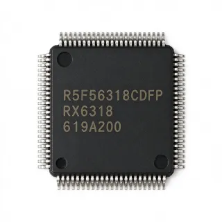
R5F562T7DDFP#V1 - 100MHz RX62T MCU 128KB Flash | Renesas
MPN: R5F562T7DDFP#V1 ✓ Active| Qty | Unit Price | Extended |
|---|---|---|
| 1 | $11.2 | $11.20 |
| 10 | $10.05 | $100.50 |
| 100 | $8.95 | $895.00 |
| 500 | $8.1 | $4,050.00 |
| 1,000 | $7.3 | $7,300.00 |
R5F562T7DDFP#V1 Overview
A 32-bit microcontroller (MCU) is a programmable processor-on-a-chip that integrates CPU core, non-volatile program memory, working RAM, and a wide variety of analog and digital peripherals onto a single silicon die. Within the broader electronics taxonomy, MCUs sit under microcontrollers -> microprocessors -> embedded processors -> semiconductors, and they are the central computational element in nearly every modern electronic product from washing machines to industrial robots. The RX62T family specifically belongs to the RX600 Series, Renesas's high-performance RX CPU architecture that targets real-time control applications with CISC-style instruction set and deterministic interrupt handling.
Key features include 165 DMIPS core performance, hardware FPU for floating-point motor-control math, dual A/D converter subsystems (12-bit high-speed + 10-bit auxiliary), 100-pin LFQFP package, supply voltage of 4.0V to 5.5V, and built-in safety features targeting IEC60730 compliance for home appliances. The integrated MTU3 and GPT timers can drive three-phase PWM outputs directly, eliminating external logic for variable-frequency drives.
The RX62T architecture uses a Harvard-style CISC core with 32-bit registers, hardware multiply-accumulate (MAC), and a single-precision IEEE-754 FPU. This combination delivers deterministic execution timing critical for field-oriented control (FOC) loops running at 16 kHz or higher. The 128 KB flash is supported by 8 KB SRAM, providing adequate headroom for sensorless-FOC firmware with observer algorithms.
Typical applications include three-phase motor drives (BLDC, PMSM, ACIM), home appliance motor control (washing machines, refrigerators, air conditioners), industrial servo drives, and fans/pumps. The on-chip dual A/D allows simultaneous sampling of phase currents and DC-bus voltage within a few hundred nanoseconds.
When designing with this part, allocate the 100-pin LFQFP footprint and use the Renesas e2studio or CS+ toolchain with the RX compiler. Reserve one of the on-chip 12-bit A/D channels for DC-bus sensing and dedicate the GPT/MTU3 channels for inverter PWM generation; this avoids software latency in the current-sense path.
This page synthesizes distributor pricing, same-brand drop-in alternatives (R5F562T7DDFP#V0, R5F562T7DDFP#11), and practical motor-control design notes not found in the manufacturer datasheet alone.
Drop-in alternatives for R5F562T7DDFP#V1 — same package, pin-to-pin compatible. Different-package parts requiring PCB rework are excluded.
Variants in this series
Same-series models that are drop-in compatible with R5F562T7DDFP#V1 (same form factor and footprint) — differing in Program Memory (Flash), SRAM.
Quick Comparison Tool — Select alternative parts for side-by-side comparison:
R5F562T7DDFP#V0
✅ Drop-In📋 Reference alternative (not in catalog)
R5F562T7DDFP#11
✅ Drop-In📋 Reference alternative (not in catalog)
R5F562T8DDFP
✅ Drop-In📋 Reference alternative (not in catalog)
R5F562N8DDFP
✅ Drop-In ⚠️ Specs Unverified📋 Reference alternative (not in catalog)
R5F562T7DDFP#V1 Maximum Ratings & Electrical Characteristics
| Core | RX600 Series RXv1 (32-bit CISC with FPU) |
| Maximum Clock Frequency | 100 MHz |
| Core Performance | 165 DMIPS |
| Program Memory (Flash) | 128 KB (128K x 8) |
| SRAM | 8 KB |
| Supply Voltage (Vcc) | 4.0 V to 5.5 V |
| High-Speed A/D Converter | 12-bit |
| Auxiliary A/D Converter | 10-bit |
| Motor-Control Timers | MTU3 + GPT |
| I/O Ports | 61 (per Renesas datasheet) |
| Package | 100-LFQFP (14x14 mm) |
| Mounting Type | Surface Mount |
| Operating Temperature | -40C to +85C (industrial) |
| Compliance Target | IEC60730 (home appliance safety) |
| Bit Width | 32-bit |
R5F562T7DDFP#V1 Pin Configuration
| Pin 1 | VREF — A/D converter reference voltage |
| Pin 2 | AVCC — Analog supply voltage |
| Pin 3 | P10_0/AN000 — Port 10 bit 0 / A/D analog input 0 |
| Pin 4 | P10_1/AN001 — Port 10 bit 1 / A/D analog input 1 |
| Pin 5 | P10_2/AN002 — Port 10 bit 2 / A/D analog input 2 |
| Pin 6 | P10_3/AN003 — Port 10 bit 3 / A/D analog input 3 |
| Pin 7 | P10_4/AN004 — Port 10 bit 4 / A/D analog input 4 |
| Pin 8 | P10_5/AN005 — Port 10 bit 5 / A/D analog input 5 |
| Pin 9 | P10_6/AN006 — Port 10 bit 6 / A/D analog input 6 |
| Pin 10 | P10_7/AN007 — Port 10 bit 7 / A/D analog input 7 |
| Pin 11 | AVSS — Analog ground |
| Pin 12 | P11_0/AN008 — Port 11 bit 0 / A/D analog input 8 |
| Pin 13 | P11_1/AN009 — Port 11 bit 1 / A/D analog input 9 |
| Pin 14 | P11_2/AN010 — Port 11 bit 2 / A/D analog input 10 |
| Pin 15 | P11_3/AN011 — Port 11 bit 3 / A/D analog input 11 |
| Pin 16 | P11_4/AN012 — Port 11 bit 4 / A/D analog input 12 |
| Pin 17 | P11_5/AN013 — Port 11 bit 5 / A/D analog input 13 |
| Pin 18 | P11_6/AN014 — Port 11 bit 6 / A/D analog input 14 |
| Pin 19 | P11_7/AN015 — Port 11 bit 7 / A/D analog input 15 |
| Pin 20 | VSS — Digital ground |
| Pin 21 | P00_0 — Port 0 bit 0 (digital I/O) |
| Pin 22 | P00_1 — Port 0 bit 1 (digital I/O) |
| Pin 23 | P00_2 — Port 0 bit 2 (digital I/O) |
| Pin 24 | P00_3 — Port 0 bit 3 (digital I/O) |
| Pin 25 | P00_4 — Port 0 bit 4 (digital I/O) |
| Pin 26 | P00_5 — Port 0 bit 5 (digital I/O) |
| Pin 27 | P00_6 — Port 0 bit 6 (digital I/O) |
| Pin 28 | P00_7 — Port 0 bit 7 (digital I/O) |
| Pin 29 | P01_0 — Port 1 bit 0 (digital I/O) |
| Pin 30 | P01_1 — Port 1 bit 1 (digital I/O) |
| Pin 31 | P01_2 — Port 1 bit 2 (digital I/O) |
| Pin 32 | P01_3 — Port 1 bit 3 (digital I/O) |
| Pin 33 | P01_4 — Port 1 bit 4 (digital I/O) |
| Pin 34 | P01_5 — Port 1 bit 5 (digital I/O) |
| Pin 35 | P01_6 — Port 1 bit 6 (digital I/O) |
| Pin 36 | P01_7 — Port 1 bit 7 (digital I/O) |
| Pin 37 | VCC — Digital supply voltage |
| Pin 38 | P02_0 — Port 2 bit 0 (digital I/O) |
| Pin 39 | P02_1 — Port 2 bit 1 (digital I/O) |
| Pin 40 | P02_2 — Port 2 bit 2 (digital I/O) |
| Pin 41 | P02_3 — Port 2 bit 3 (digital I/O) |
| Pin 42 | P02_4 — Port 2 bit 4 (digital I/O) |
| Pin 43 | P02_5 — Port 2 bit 5 (digital I/O) |
| Pin 44 | P02_6 — Port 2 bit 6 (digital I/O) |
| Pin 45 | P02_7 — Port 2 bit 7 (digital I/O) |
| Pin 46 | P03_0 — Port 3 bit 0 (digital I/O) |
| Pin 47 | P03_1 — Port 3 bit 1 (digital I/O) |
| Pin 48 | P03_2 — Port 3 bit 2 (digital I/O) |
| Pin 49 | P03_3 — Port 3 bit 3 (digital I/O) |
| Pin 50 | P03_4 — Port 3 bit 4 (digital I/O) |
| Pin 51 | P03_5 — Port 3 bit 5 (digital I/O) |
| Pin 52 | P03_6 — Port 3 bit 6 (digital I/O) |
| Pin 53 | P03_7 — Port 3 bit 7 (digital I/O) |
| Pin 54 | VSS — Digital ground |
| Pin 55 | P04_0 — Port 4 bit 0 (digital I/O) |
| Pin 56 | P04_1 — Port 4 bit 1 (digital I/O) |
| Pin 57 | P04_2 — Port 4 bit 2 (digital I/O) |
| Pin 58 | P04_3 — Port 4 bit 3 (digital I/O) |
| Pin 59 | P04_4 — Port 4 bit 4 (digital I/O) |
| Pin 60 | P04_5 — Port 4 bit 5 (digital I/O) |
| Pin 61 | P04_6 — Port 4 bit 6 (digital I/O) |
| Pin 62 | P04_7 — Port 4 bit 7 (digital I/O) |
| Pin 63 | VCC — Digital supply voltage |
| Pin 64 | P05_0 — Port 5 bit 0 (digital I/O) |
| Pin 65 | P05_1 — Port 5 bit 1 (digital I/O) |
| Pin 66 | P05_2 — Port 5 bit 2 (digital I/O) |
| Pin 67 | P05_3 — Port 5 bit 3 (digital I/O) |
| Pin 68 | P05_4 — Port 5 bit 4 (digital I/O) |
| Pin 69 | P05_5 — Port 5 bit 5 (digital I/O) |
| Pin 70 | P05_6 — Port 5 bit 6 (digital I/O) |
| Pin 71 | P05_7 — Port 5 bit 7 (digital I/O) |
| Pin 72 | P06_0 — Port 6 bit 0 (digital I/O) |
| Pin 73 | P06_1 — Port 6 bit 1 (digital I/O) |
| Pin 74 | P06_2 — Port 6 bit 2 (digital I/O) |
| Pin 75 | P06_3 — Port 6 bit 3 (digital I/O) |
| Pin 76 | P06_4 — Port 6 bit 4 (digital I/O) |
| Pin 77 | P06_5 — Port 6 bit 5 (digital I/O) |
| Pin 78 | P06_6 — Port 6 bit 6 (digital I/O) |
| Pin 79 | P06_7 — Port 6 bit 7 (digital I/O) |
| Pin 80 | VSS — Digital ground |
| Pin 81 | P07_0 — Port 7 bit 0 (digital I/O) |
| Pin 82 | P07_1 — Port 7 bit 1 (digital I/O) |
| Pin 83 | P07_2 — Port 7 bit 2 (digital I/O) |
| Pin 84 | P07_3 — Port 7 bit 3 (digital I/O) |
| Pin 85 | P07_4 — Port 7 bit 4 (digital I/O) |
| Pin 86 | P07_5 — Port 7 bit 5 (digital I/O) |
| Pin 87 | P07_6 — Port 7 bit 6 (digital I/O) |
| Pin 88 | P07_7 — Port 7 bit 7 (digital I/O) |
| Pin 89 | P12_0 — Port 12 bit 0 (digital I/O) |
| Pin 90 | P12_1 — Port 12 bit 1 (digital I/O) |
| Pin 91 | P12_2 — Port 12 bit 2 (digital I/O) |
| Pin 92 | P12_3 — Port 12 bit 3 (digital I/O) |
| Pin 93 | P12_4 — Port 12 bit 4 (digital I/O) |
| Pin 94 | P12_5 — Port 12 bit 5 (digital I/O) |
| Pin 95 | VCC — Digital supply voltage |
| Pin 96 | RES# — Reset (active low) |
| Pin 97 | XTAL — Crystal oscillator connection |
| Pin 98 | EXTAL — External clock input / crystal connection |
| Pin 99 | VSS — Digital ground |
| Pin 100 | VCC — Digital supply voltage |
Typical Applications
R5F562T7DDFP#V1 is suitable for 7 applications: Three-Phase BLDC / PMSM Motor Drive, Home Appliance Motor Control (Washing Machines, Refrigerators), Industrial Servo Drives and Variable-Frequency Drives, Electric Vehicle (EV) Auxiliary Motor Control, Robotic Actuators and Drone BLDC Controllers, Solar Inverter and Power Conversion Control, Fan and Pump Speed Controllers.
Three-Phase BLDC / PMSM Motor Drive
The R5F562T7DDFP#V1's 100 MHz RX core with hardware FPU and integrated MTU3+GPT timers makes it ideal for three-phase BLDC and PMSM motor drives. With 165 DMIPS performance, the chip executes Park/Clarke transforms and PI control loops in real time at 16 kHz FOC rates without software bottlenecks. The 12-bit high-speed A/D converter samples phase currents within 1 us, enabling precise torque control. Drop the chip between the gate driver and current sensors; reserve one A/D channel for DC-bus sensing.
Recommended
Home Appliance Motor Control (Washing Machines, Refrigerators)
The R5F562T7DDFP#V1 is purpose-built for IEC60730-certified home appliances, integrating hardware watchdog, clock monitoring, and A/D self-test that simplify safety certification. With 128 KB flash, the MCU holds both the main motor-control algorithm and the safety library without external memory. The 100-LFQFP package fits the typical appliance control board, and the 5 V operation aligns with standard white-goods power rails. Designers can reuse this single chip across washer drum motor, drain pump, and compressor control variants.
Recommended
Industrial Servo Drives and Variable-Frequency Drives
For industrial servo and variable-frequency drives, the R5F562T7DDFP#V1 delivers the deterministic interrupt latency required for high-bandwidth current loops. The dual A/D converter (12-bit high-speed + 10-bit auxiliary) handles simultaneous sampling of phase currents, DC-bus voltage, and temperature sensors. At 100 MHz with FPU, the MCU executes model-predictive-control or field-weakening algorithms beyond what is possible on slower Cortex-M0 parts. The 100-LFQFP industrial-grade package supports -40C to +85C operation in factory cabinets.
Recommended
Electric Vehicle (EV) Auxiliary Motor Control
In EV auxiliary systems such as coolant pumps, oil pumps, and HVAC blowers, the R5F562T7DDFP#V1 provides automotive-grade motor control without the cost of full ASIL-D MCUs. The 12-bit A/D and MTU3 timers drive sensorless FOC at 8 kHz, sufficient for pump and blower applications. The 5 V supply aligns with 12 V battery rails after a linear regulator, and the 100-LFQFP withstands under-hood temperature ranges up to +85C. Pair with a CAN transceiver to integrate with the vehicle bus.
Recommended
Robotic Actuators and Drone BLDC Controllers
Robotic joint actuators and drone ESCs benefit from the R5F562T7DDFP#V1's compact 100-LFQFP form factor and 165 DMIPS performance per watt. The hardware FPU accelerates sin/cos computations used in FOC commutation, and the 12-bit A/D is fast enough for drone ESC current loops at 50 kHz PWM rates. The 128 KB flash holds both position-control and current-control firmware. The exposed pad on the LFQFP aids heat dissipation during high-current hover throttle.
Recommended
Solar Inverter and Power Conversion Control
In small solar inverters and micro-inverters, the R5F562T7DDFP#V1 controls the MPPT algorithm, grid synchronization, and inverter switching. The 100 MHz core runs the MPPT loop at 10 kHz while handling grid-frequency monitoring in the background. The 10-bit auxiliary A/D can measure grid voltage and DC-bus simultaneously, and the MTU3 timers generate the inverter PWM. The IEC60730 safety features add arc-fault detection logic for residential solar installations.
Recommended
Fan and Pump Speed Controllers
For HVAC fans, industrial blowers, and water-pump speed controllers, the R5F562T7DDFP#V1 provides sufficient processing for closed-loop PI speed control with smooth ramp profiles. The 128 KB flash is generous for application code including fault logging, while 8 KB SRAM handles the runtime state. The 100-LFQFP package drops onto standard 4-layer appliance boards, and the IEC60730 features help meet residential safety requirements without external supervisor ICs.
Recommended
Recommended Products Summary
Engineering reference data for R5F562T7DDFP#V1 — comparison, design guidance, and compliance information.
Selection Guide
Comparison with Alternatives
| Parameter | This Product | R5F562T7DDFP#V0 | R5F562T7DDFP#11 | R5F562T8DDFP | R5F562N8DDFP |
|---|---|---|---|---|---|
| Brand | Renesas Electronics | Renesas Electronics | Renesas Electronics | Renesas Electronics | Renesas Electronics |
| Package | 100-LFQFP (14x14 mm) | 100-LFQFP (14x14 mm) - same | 100-LFQFP (14x14 mm) - same | 100-LFQFP (14x14 mm) - same | 100-LFQFP (14x14 mm) - same |
| Program Flash | 128 KB | 128 KB | 128 KB | 256 KB | 256 KB |
| SRAM | 8 KB | 8 KB | 8 KB | 16 KB | 16 KB |
| Maximum Clock | 100 MHz | 100 MHz | 100 MHz | 100 MHz | 100 MHz |
| Core Performance | 165 DMIPS | 165 DMIPS | 165 DMIPS | 165 DMIPS | 165 DMIPS |
| A/D Converter | 12-bit + 10-bit | 12-bit + 10-bit | 12-bit + 10-bit | 12-bit + 10-bit | 12-bit + 10-bit |
| Supply Voltage | 4.0V to 5.5V | 4.0V to 5.5V | 4.0V to 5.5V | 4.0V to 5.5V | 3.0V to 3.6V |
| IEC60730 Safety | Yes (target) | Yes | Yes | Yes | No (different family) |
Key Differentiators
- On-chip 12-bit + 10-bit dual A/D converter for simultaneous phase-current sampling (vs R5F562N8DDFP)
- Hardware FPU for FOC algorithm acceleration (vs R5F562T7DDFP#V0)
- Built-in IEC60730 safety features for home appliances (vs R5F562T7DDFP#11)
Design Notes
Estimated: At VCC=5V and core activity at 100 MHz with peripheral toggling, the R5F562T7DDFP#V1 draws approximately 50-70 mA active current. Add a 10 uF bulk capacitor plus 0.1 uF ceramic decoupling close to each VCC/VSS pin (the package has 4 VCC and 3 VSS pins distributed around the LFQFP). Power the AVCC pin from the same 5 V rail through a ferrite bead to isolate analog noise from the switching digital domains.
Estimated: The 100-LFQFP package has a typical theta_JA of approximately 50 C/W on a 4-layer JEDEC test board. At 70 mA and 5 V (350 mW active), junction temperature rise above ambient is roughly 17.5 C, well within the -40C to +85C industrial rating. For continuous high-activity inverter-control use cases, add a copper pour under the exposed pad to keep junction below 100 C.
Route the MTU3 and GPT PWM output traces (P00_0 through P00_5 typically) as matched-length differential pairs to the gate driver inputs to avoid timing skew between high-side and low-side switching. Keep the analog A/D traces (P10 and P11) away from PWM switching nodes by at least 3x the trace width to minimize coupled noise. Place the XTAL/EXTAL traces short and symmetric, and surround the crystal with a ground guard ring.
Do not connect the AVCC pin directly to VCC without a ferrite bead - this couples digital switching noise into the 12-bit A/D reference and degrades current-sensing accuracy. Do not leave the RES# pin floating; tie it through a 10 kohm pull-up to VCC and a 1 nF capacitor to VCC for proper reset behavior. When migrating from R5F562T7 to R5F562T8, verify the linker script accommodates the doubled flash and SRAM regions.
The 100-LFQFP 14x14 mm package has 0.65 mm pitch, which is at the edge of standard 6-mil trace + space capability. Use 5-mil trace and 5-mil space rules for escape routing under the package, with via-in-pad if your fab supports it. Place a continuous ground plane on layer 2 directly under the MCU, with the exposed pad stitched to ground with at least 9 thermal vias for heat spreading.
Compliance Information
RoHS and halogen-free per Renesas product page. IEC60730 safety target supported but not AEC-Q100 qualified. Lead-free assembly compatible.