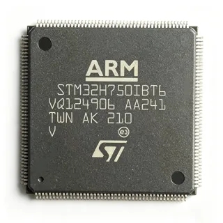
SPC5646CF0MLU1 - 32-bit Dual-Core 3MB Flash 120MHz MCU | NXP
MPN: SPC5646CF0MLU1 ✓ Active| Qty | Unit Price | Extended |
|---|---|---|
| 1 | $35.81 | $35.81 |
| 10 | $34.2 | $342.00 |
| 100 | $32.1 | $3,210.00 |
| 500 | $30.4 | $15,200.00 |
| 1,000 | $28.65 | $28,650.00 |
SPC5646CF0MLU1 Overview
A microcontroller (MCU) is a single-chip computer integrating a processor core, memory, and peripherals such as timers, communication interfaces, and ADCs. Within the embedded-system hierarchy, the SPC5646CF0MLU1 sits in the high-end segment: an automotive MCU built on the Power Architecture (e200) core family, one tier above general-purpose 8-bit and entry 32-bit MCUs, and it belongs to NXP's MPC564xB-C family aimed at enhanced feature sets and large memory space in vehicle electronics.
Key features include dual-core lockstep-capable processing for safety-oriented designs, 3 MB of program flash that supports feature-rich gateway and body-control firmware, 256 KB of SRAM for buffers and stacks, and an industrial -40C to +125C operating range. The part is specified by NXP as automotive grade, addressing body control module (BCM), gateway, and industrial applications with secure and trusted data transmission support.
Technical depth: the e200z4d core is a Power Architecture Book E 32-bit CPU with a seven-stage pipeline and VLE (Variable Length Encoding) support for code density; the secondary e200z0h core offloads communication and housekeeping tasks, increasing effective throughput without raising the main core's interrupt load. Low-power standby and wait modes reduce consumption in always-on vehicle domains where the module must wake on network traffic (per NXP family overview).
Typical applications include automotive body control modules, vehicle gateway ECUs that bridge CAN/LIN/FlexRay domains, and industrial control systems requiring large flash and extended temperature range.
Design consideration: verify the exact flash size and temperature variant suffix (CF0, 3 MB, -40/+125C) against your BOM, since the MPC564xB-C family shares one footprint across many memory grades; the 176-LQFP allows board reuse across family members.
This page synthesizes distributor pricing, drop-in family alternatives, and practical design notes not found in the manufacturer datasheet, with pricing references as of 2026-10-18.
Drop-in alternatives for SPC5646CF0MLU1 — same package, pin-to-pin compatible. Different-package parts requiring PCB rework are excluded.
Variants in this series
Same-series models that are drop-in compatible with SPC5646CF0MLU1 (same form factor and footprint) — differing in Core Processor, Grade, Series, Core Size, Package.
Quick Comparison Tool — Select alternative parts for side-by-side comparison:
SPC5646CCF0MLU1
✅ Drop-In📋 Reference alternative (not in catalog)
SPC5645CF0MLU1
✅ Drop-In📋 Reference alternative (not in catalog)
SPC5646BK0MLU1
✅ Drop-In📋 Reference alternative (not in catalog)
SPC5644CF0VLU1
✅ Drop-In📋 Reference alternative (not in catalog)
SPC5644AF0MLU2
✅ Drop-In ⚠️ Specs Unverified✓ In Stock
$12.5 / Unit
View Datasheet →SPC5642AF2MLU1
✅ Drop-In ⚠️ Specs Unverified✓ In Stock
$21.23 / Unit
View Datasheet →SPC5646CF0MLU1 Maximum Ratings & Electrical Characteristics
| Core Processor | e200z4d + e200z0h (Power Architecture) |
| Core Size | 32-Bit Dual-Core |
| Main Core Speed | 120 MHz |
| Auxiliary Core Speed | 80 MHz |
| Flash Memory | 3 MB (3M x 8) |
| RAM Size | 256 KB |
| Series | MPC56xx Qorivva (MPC564xB-C family) |
| Operating Temperature | -40C to +125C |
| Package | 176-LQFP (24x24 mm) |
| Mounting Type | Surface Mount |
| Terminal Form | Gull Wing |
| Grade | Automotive |
| Application Class | Body Control Module, Gateway, Industrial |
| Low-Power Modes | Standby / Wait modes |
| Security Features | Secure and trusted transmission support |
SPC5646CF0MLU1 176-lqfp (24x24 mm) Pin Configuration Guide
Pin configuration for SPC5646CF0MLU1 (176-lqfp (24x24 mm) package). This digital IC includes GPIO, communication interfaces (UART, SPI, I2C), and power pins. Refer to the manufacturer datasheet for alternate pin functions and configuration options. Essential for embedded system design and PCB layout.

No detailed pinout data available for SPC5646CF0MLU1.
Refer to the datasheet for full pin configuration.
Typical Applications
SPC5646CF0MLU1 is suitable for 6 applications: Automotive Body Control Module (BCM), Vehicle Gateway ECU, Industrial Control Systems, Domain Controller / Chassis Electronics, Telematics and Secure Communication Units, Gateway-Integrated Battery Management Frontends (48V Mild Hybrid).
Automotive Body Control Module (BCM)
The SPC5646CF0MLU1 fits body control modules because NXP explicitly positions the MPC564xB-C family for high-end BCM designs, and its 3 MB flash accommodates consolidated lighting, wiper, seat, and access-control firmware that previously required multiple smaller ECUs. In a BCM, the 120 MHz e200z4d core executes application logic and diagnostics while the 80 MHz e200z0h core services LIN and CAN frames, reducing interrupt load on the main core. The -40C to +125C range covers under-hood-adjacent zones, and low-power standby/wait modes keep quiescent draw acceptable for always-on battery-connected modules that must wake on network activity. The 176-LQFP footprint provides enough GPIO for relay and LED driver banks.
Recommended
Vehicle Gateway ECU
Gateways bridge CAN, LIN, and FlexRay domains, and the SPC5646CF0MLU1's dual-core architecture maps directly onto this workload: the 120 MHz e200z4d runs routing tables, diagnostics (UDS), and firewalling, while the e200z0h handles physical-layer message queuing. Its 256 KB RAM buffers bursty network traffic across domains, and 3 MB flash stores firmware plus OTA-staged images and calibration sets. NXP highlights 'secure and trusted transmission of information between parties' for this family, addressing gateway security requirements. Because pin-compatible family members exist in the same LQFP-176 package, gateway platforms can scale memory across vehicle trim levels without PCB respins, a major program-cost advantage.
Recommended
Industrial Control Systems
NXP lists industrial applications alongside automotive BCM/gateway for the MPC564xB-C family, and the SPC5646CF0MLU1 suits factory automation controllers that need large program memory and extended temperature range. The -40C to +125C rating survives cabinet environments without forced cooling, and the 3 MB flash supports protocol stacks (PROFINET/CANopen-style fieldbus gateways), logging, and IEC-style application layers. The dual-core split lets one core run the real-time control loop while the other manages communications and HMI data exchange. Its gull-wing 176-LQFP terminals are reworkable with standard hot-air tools, supporting the small-batch production and field-repair patterns common in industrial equipment.
Recommended
Domain Controller / Chassis Electronics
As vehicle architectures consolidate, chassis-domain controllers merge suspension, steering-support, and stability-adjacent logic into one ECU. The SPC5646CF0MLU1's automotive-grade qualification, 120 MHz dual-core throughput, and 3 MB flash make it a fit for consolidated chassis modules where the previous generation needed multiple 512 KB-class MCUs. The e200z4d's pipeline executes control-loop and diagnostic code deterministically, while the auxiliary core isolates safety-monitoring housekeeping. Its low-power standby modes support the kl15-off current budgets that OEMs impose, and the shared MPC56xx software ecosystem (drivers, AUTOSAR MCALs) shortens integration time compared with adopting a new architecture mid-program.
Recommended
Telematics and Secure Communication Units
Telematics control units demand large code space for connectivity stacks and secure key handling; the SPC5646CF0MLU1 provides 3 MB flash plus NXP's family-level 'secure and trusted transmission of information between parties' support. In a TCU, the main core manages the modem interface, certificate handling, and application logic, while the e200z0h core services CAN gateways to vehicle networks. The 256 KB RAM holds TLS-style session buffers and message queues. Its automotive temperature range and Qorivva heritage make it acceptable for OEM-grade telematics programs where consumer-grade application processors are disqualified by qualification requirements and longevity commitments.
Recommended
Gateway-Integrated Battery Management Frontends (48V Mild Hybrid)
Mild-hybrid 48V systems need a central controller that talks to the vehicle gateway while managing battery monitoring frontends. The SPC5646CF0MLU1's large flash holds state-of-charge estimation code, ISO 26262-style monitoring software, and communication stacks simultaneously. The dual-core split is valuable here: one core runs estimation and balancing control at fixed rate, the other handles CAN/FlexRay exchange with the powertrain domain. Its -40C to +125C range suits battery-box-mounted locations, and standby/wait modes meet the parked-vehicle drain targets that battery-management modules must meet. Using an automotive-qualified MCU avoids requalification risk when consumer MCUs are proposed for cost reduction.
Recommended
Recommended Products Summary
Engineering reference data for SPC5646CF0MLU1 — comparison, design guidance, and compliance information.
Selection Guide
Comparison with Alternatives
| Parameter | This Product | SPC5646CCF0MLU1 | SPC5645CF0MLU1 | SPC5646BK0MLU1 | SPC5644CF0VLU1 |
|---|---|---|---|---|---|
| Package | 176-LQFP (24x24 mm) | 176-LQFP (24x24) - same | 176-LQFP (24x24) - same | 176-LQFP - same | 176-QFP - same footprint |
| Brand | NXP Semiconductors | NXP Semiconductors | NXP Semiconductors | NXP Semiconductors | NXP Semiconductors |
| Core Architecture | 32-bit dual-core e200z4d + e200z0h | e200 family, same class | e200 family | e200/e200z4 family | e200z4 family |
Key Differentiators
- 3 MB flash for consolidated BCM/gateway firmware (vs SPC5646BK0MLU1)
- -40C to +125C automotive M-grade rating (vs SPC5644CF0VLU1)
- True dual-core (120 MHz e200z4d + 80 MHz e200z0h) task partitioning (vs SPC5645CF0MLU1)
Design Notes
The 176-LQFP (24x24 mm) gull-wing package requires a 0.5 mm pitch land pattern per the NXP datasheet footprint; use solder-mask-defined pads with ~0.1 mm expansion to improve paste release. Place 100 nF ceramic decoupling capacitors at all VDD pin pairs, within 2 mm of the pins, plus bulk 10 uF at the supply entry. Expose adequate ground pour under the package and use multiple thermal vias to the ground plane. The gull-wing leads allow visual AOI inspection of all four sides, which simplifies automotive production quality gates.
The MPC56xx family typically uses separate core and I/O supply rails; consult the manufacturer datasheet for the exact voltage domains and sequencing requirements before power-tree design. Estimated power: at 120 MHz, core current in the tens-to-hundreds of mA range should be assumed for regulation sizing until the datasheet typical ICC figures are confirmed - design the core regulator with headroom and verify standby-mode current against the module's kl15-off budget. Use POR/brown-out supervision and gate the reset release until all rails are stable.
Do not treat MPC564xB-C family members as interchangeable without checking the memory suffix: SPC5646CF0 (3 MB), SPC5646BK0, and SPC5645 grades differ in flash density and possibly peripheral sets, and the temperature suffix (M = -40/+125C, V grades differ) matters for automotive qualification. Also confirm NXP product change notices (available on the NXP product page) for die revisions before production, and verify that your flash programming algorithm and calibration data match the specific derivative to avoid boot failures.
Compliance Information
Distributor listings show a RoHS field for this part and NXP markets it as Automotive Grade. Verify REACH, halogen-free, and conflict-minerals declarations via NXP's official Environmental Quality documents on the product page; official AEC-Q100 self-certification documentation should be requested from NXP for regulated programs.