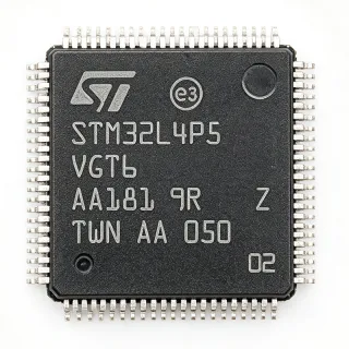
STM32F205VGT6 - 120MHz ARM Cortex-M3 MCU 1MB Flash | STMicroelectronics
MPN: STM32F205VGT6 ✓ Active| Qty | Unit Price | Extended |
|---|---|---|
| 1 | $12.5 | $12.50 |
| 10 | $11.2 | $112.00 |
| 100 | $9.75 | $975.00 |
| 500 | $8.85 | $4,425.00 |
| 1,000 | $8.1 | $8,100.00 |
STM32F205VGT6 Overview
An ARM Cortex-M3 microcontroller (MCU) is a 32-bit RISC processor core designed by Arm for embedded systems, featuring deterministic interrupt latency, Thumb-2 instruction set, and optional hardware multiply-accumulate. Within the broader taxonomy, the Cortex-M3 sits under Arm Cortex-M → 32-bit MCU → embedded microcontroller → semiconductor IC. The STM32F2 family specifically targets applications that require high computational throughput plus rich connectivity (USB OTG, Ethernet, CAN, SDIO) without the higher cost of Cortex-M4 parts.
Key features include 82 GPIO pins, three 12-bit ADCs (up to 2.4 MSPS), two 12-bit DACs, 17 timers, USB OTG Full-Speed and High-Speed, 10/100 Ethernet MAC, two CAN 2.0B controllers, an SDIO interface, and a camera interface. The integrated 4 KB backup SRAM retains data in standby mode while consuming only a few microamperes, and the part supports four low-power modes (Sleep, Stop, Standby, and VBAT) for battery-powered designs.
The architecture uses a multi-AHB bus matrix with separate buses for SRAM, Flash, and peripherals, allowing parallel DMA transfers and Cortex-M3 core execution without contention. The 120 MHz clock is sourced from an internal 16 MHz RC oscillator (with PLL) or an external 4-26 MHz crystal, enabling flexible system clock trees. Cryptographic and FSMC functions are NOT included on the F205 sub-line (those land on the F207 sub-line), which keeps this part cost-optimized for non-crypto applications.
Typical applications include industrial control (PLCs, motor drives, factory automation), medical equipment (patient monitors, diagnostic peripherals), consumer electronics (home appliances, audio devices with USB), networking (Ethernet-enabled IoT gateways, smart sensors), and human-machine interfaces (touchscreen controllers, graphical displays). The 1 MB Flash and 132 KB SRAM also suit firmware-over-the-air (FOTA) updates with rollback image storage.
When designing with the STM32F205VGT6, ensure your PCB layout places the 100-pin LQFP's exposed pad (if present on the variant) onto a ground copper pour for thermal dissipation, and follow ST's application note AN2867 for oscillator PCB layout. Decouple VDD/VDDA/VBAT with 100 nF ceramic capacitors placed within 2 mm of each supply pin, and add a 4.7 uF bulk capacitor per supply rail. VDD operating range is 1.8-3.6 V (the V suffix), so verify your LDO selection covers this range with adequate transient response.
This page synthesizes distributor pricing, drop-in pin-compatible alternatives, and practical design notes not found in the manufacturer datasheet alone, helping engineers evaluate second-source options and PCB migration paths for the STM32F205VGT6.
Drop-in alternatives for STM32F205VGT6 — same package, pin-to-pin compatible. Different-package parts requiring PCB rework are excluded.
Variants in this series
Same-series models that are drop-in compatible with STM32F205VGT6 (same form factor and footprint) — differing in Package, SRAM, Flash Memory, Operating Temperature Range, Timers.
Quick Comparison Tool — Select alternative parts for side-by-side comparison:
STM32F207VGT6
✅ Drop-In✓ In Stock
$6.8182 / Unit
View Datasheet →STM32F205VET7
✅ Drop-In✓ In Stock
$8.95 / Unit
View Datasheet →GD32F205VGT6
✅ Drop-In📋 Reference alternative (not in catalog)
STM32F207VFT6
✅ Drop-In📋 Reference alternative (not in catalog)
STM32F205VGT6 Maximum Ratings & Electrical Characteristics
| Core | ARM Cortex-M3 32-bit RISC |
| Maximum Clock Frequency | 120 MHz |
| Performance | 150 DMIPs |
| Flash Memory | 1 MB (1M x 8) |
| SRAM | 132 KB |
| Number of I/O Pins | 82 |
| Package | 100-LQFP (14x14 mm) |
| Supply Voltage Range | 1.8 V to 3.6 V |
| ADC | 3x 12-bit, up to 2.4 MSPS |
| DAC | 2x 12-bit |
| Timers | 17 (including 1 systick) |
| Communication Interfaces | USB OTG HS/FS, 10/100 Ethernet, 2x CAN 2.0B, 3x SPI, 3x I2C, 6x USART/UART, SDIO |
| Camera Interface | Yes (8/10/12/14-bit) |
| FSMC | Yes (external memory bus) |
| Cryptographic Accelerator | No (not present on F205 line) |
| Operating Temperature Range | -40C to +85C (grade 6) |
| Mounting Type | Surface Mount (LQFP) |
| RoHS Status | Compliant |
STM32F205VGT6 Pin Configuration
| Pin 1 | PE2 — GPIO PE2 / TRACECLK / FSMC_A23 |
| Pin 2 | PE3 — GPIO PE3 / TRACED0 / FSMC_A19 |
| Pin 3 | PE4 — GPIO PE4 / TRACED1 / FSMC_A20 |
| Pin 4 | PE5 — GPIO PE5 / TRACED2 / FSMC_A21 |
| Pin 5 | PE6 — GPIO PE6 / TRACED3 / FSMC_A22 |
| Pin 6 | VBAT — Battery domain supply for RTC and backup SRAM |
| Pin 7 | PC13 — GPIO PC13 / RTC_TAMP1 (anti-tamper) |
| Pin 8 | PC14 — GPIO PC14 / OSC32_IN (LSE crystal) |
| Pin 9 | PC15 — GPIO PC15 / OSC32_OUT (LSE crystal) |
| Pin 10 | VSS — Digital ground |
| Pin 11 | VDD — Digital supply 1.8-3.6V |
| Pin 12 | OSC_IN — HSE crystal input (4-26 MHz) |
| Pin 13 | OSC_OUT — HSE crystal output |
| Pin 14 | NRST — Reset input (active low) |
| Pin 15 | PC0 — GPIO PC0 / ADC123_IN10 |
| Pin 16 | PC1 — GPIO PC1 / ADC123_IN11 |
| Pin 17 | PC2 — GPIO PC2 / ADC123_IN12 |
| Pin 18 | PC3 — GPIO PC3 / ADC123_IN13 |
| Pin 19 | VREF+ — ADC positive reference |
| Pin 20 | VSSA — Analog ground |
| Pin 21 | VDDA — Analog supply 1.8-3.6V |
| Pin 22 | PA0 — GPIO PA0 / WKUP / TIM2_CH1 / ADC123_IN0 |
| Pin 23 | PA1 — GPIO PA1 / TIM2_CH2 / ADC123_IN1 |
| Pin 24 | PA2 — GPIO PA2 / USART2_TX / TIM5_CH3 / ADC123_IN2 |
| Pin 25 | PA3 — GPIO PA3 / USART2_RX / TIM5_CH4 / ADC123_IN3 |
| Pin 26 | VSS — Digital ground |
| Pin 27 | VDD — Digital supply 1.8-3.6V |
| Pin 28 | PA4 — GPIO PA4 / SPI1_NSS / USART2_CK / DAC_OUT1 / ADC12_IN4 |
| Pin 29 | PA5 — GPIO PA5 / SPI1_SCK / DAC_OUT2 / ADC12_IN5 |
| Pin 30 | PA6 — GPIO PA6 / SPI1_MISO / TIM3_CH1 / ADC12_IN6 |
| Pin 31 | PA7 — GPIO PA7 / SPI1_MOSI / TIM3_CH2 / ADC12_IN7 |
| Pin 32 | PB0 — GPIO PB0 / TIM3_CH3 / ADC12_IN8 |
| Pin 33 | PB1 — GPIO PB1 / TIM3_CH4 / ADC12_IN9 |
| Pin 34 | PB2 — GPIO PB2 / BOOT1 |
| Pin 35 | PB10 — GPIO PB10 / I2C2_SCL / USART3_TX / FSMC_D10 |
| Pin 36 | PB11 — GPIO PB11 / I2C2_SDA / USART3_RX / FSMC_D11 |
| Pin 37 | VSS — Digital ground |
| Pin 38 | VDD — Digital supply 1.8-3.6V |
| Pin 39 | PB12 — GPIO PB12 / SPI2_NSS / I2C2_SMBAI / FSMC_D12 |
| Pin 40 | PB13 — GPIO PB13 / SPI2_SCK / FSMC_D13 |
| Pin 41 | PB14 — GPIO PB14 / SPI2_MISO / USB_HS_DM |
| Pin 42 | PB15 — GPIO PB15 / SPI2_MOSI / USB_HS_DP |
| Pin 43 | PD8 — GPIO PD8 / FSMC_D14 |
| Pin 44 | PD9 — GPIO PD9 / FSMC_D15 |
| Pin 45 | PD10 — GPIO PD10 / FSMC_FMCLE |
| Pin 46 | PD11 — GPIO PD11 / FSMC_FMCNR |
| Pin 47 | PD12 — GPIO PD12 / FSMC_A16 / TIM4_CH1 |
| Pin 48 | PD13 — GPIO PD13 / FSMC_A17 / TIM4_CH2 |
| Pin 49 | VSS — Digital ground |
| Pin 50 | VDD — Digital supply 1.8-3.6V |
| Pin 51 | PD14 — GPIO PD14 / FSMC_D0 |
| Pin 52 | PD15 — GPIO PD15 / FSMC_D1 / TIM4_CH4 |
| Pin 53 | PG2 — GPIO PG2 / FSMC_A12 |
| Pin 54 | PG3 — GPIO PG3 / FSMC_A13 |
| Pin 55 | PG4 — GPIO PG4 / FSMC_A14 |
| Pin 56 | PG5 — GPIO PG5 / FSMC_A15 |
| Pin 57 | PG6 — GPIO PG6 / FSMC_INT2 |
| Pin 58 | PG7 — GPIO PG7 / FSMC_INT3 |
| Pin 59 | PG8 — GPIO PG8 |
| Pin 60 | VSS — Digital ground |
| Pin 61 | VDD — Digital supply 1.8-3.6V |
| Pin 62 | PC6 — GPIO PC6 / TIM3_CH1 / USART6_TX / FSMC_NWAIT / SDIO_D6 |
| Pin 63 | PC7 — GPIO PC7 / TIM3_CH2 / USART6_RX / FSMC_NE3 / SDIO_D7 |
| Pin 64 | PC8 — GPIO PC8 / TIM3_CH3 / USART6_CK / SDIO_D0 |
| Pin 65 | PC9 — GPIO PC9 / TIM3_CH4 / I2C3_SDA / SDIO_D1 |
| Pin 66 | PA8 — GPIO PA8 / USART1_CK / TIM1_CH1 / MCO1 |
| Pin 67 | PA9 — GPIO PA9 / USART1_TX / TIM1_CH2 / OTG_FS_VBUS |
| Pin 68 | PA10 — GPIO PA10 / USART1_RX / TIM1_CH3 / OTG_FS_ID |
| Pin 69 | PA11 — GPIO PA11 / USART1_CTS / CAN1_RX / OTG_FS_DM |
| Pin 70 | PA12 — GPIO PA12 / USART1_RTS / CAN1_TX / OTG_FS_DP |
| Pin 71 | PA13 — GPIO PA13 / JTMS-SWDIO |
| Pin 72 | VSS — Digital ground |
| Pin 73 | VDD — Digital supply 1.8-3.6V |
| Pin 74 | PA14 — GPIO PA14 / JTCK-SWCLK |
| Pin 75 | PA15 — GPIO PA15 / JTDI / SPI3_NSS / TIM2_CH1_ETR |
| Pin 76 | PC10 — GPIO PC10 / UART4_TX / FSMC_NE2 / SDIO_D2 |
| Pin 77 | PC11 — GPIO PC11 / UART4_RX / FSMC_NCE4_1 / SDIO_D3 |
| Pin 78 | PC12 — GPIO PC12 / UART5_TX / FSMC_CLE / SDIO_CK |
| Pin 79 | PD0 — GPIO PD0 / FSMC_D2 / CAN1_RX |
| Pin 80 | PD1 — GPIO PD1 / FSMC_D3 / CAN1_TX |
| Pin 81 | PD2 — GPIO PD2 / TIM3_ETR / UART5_RX / SDIO_CMD |
| Pin 82 | PD3 — GPIO PD3 / FSMC_CLK |
| Pin 83 | PD4 — GPIO PD4 / FSMC_NOE |
| Pin 84 | PD5 — GPIO PD5 / FSMC_NWE |
| Pin 85 | VSS — Digital ground |
| Pin 86 | VDD — Digital supply 1.8-3.6V |
| Pin 87 | PD6 — GPIO PD6 / FSMC_NWAIT / UART2_RX |
| Pin 88 | PD7 — GPIO PD7 / FSMC_NCE2 / UART2_TX |
| Pin 89 | PB3 — GPIO PB3 / JTDO / SPI3_SCK / TIM2_CH2 |
| Pin 90 | PB4 — GPIO PB4 / NJTRST / SPI3_MISO / TIM3_CH1 |
| Pin 91 | PB5 — GPIO PB5 / SPI3_MOSI / I2C1_SMBAI / TIM3_CH2 |
| Pin 92 | PB6 — GPIO PB6 / I2C1_SCL / TIM4_CH1 / USART1_TX |
| Pin 93 | PB7 — GPIO PB7 / I2C1_SDA / TIM4_CH2 / USART1_RX |
| Pin 94 | BOOT0 — Boot mode select (0=Flash, 1=System memory bootloader) |
| Pin 95 | PB8 — GPIO PB8 / TIM4_CH3 / I2C1_SCL / CAN1_RX |
| Pin 96 | PB9 — GPIO PB9 / TIM4_CH4 / I2C1_SDA / CAN1_TX |
| Pin 97 | PE0 — GPIO PE0 / TIM4_ETR / FSMC_NBL0 |
| Pin 98 | PE1 — GPIO PE1 / FSMC_NBL1 |
| Pin 99 | VSS — Digital ground |
| Pin 100 | VDD — Digital supply 1.8-3.6V |
Typical Applications
STM32F205VGT6 is suitable for 7 applications: Industrial Motor Control, Medical Patient Monitoring, Ethernet-Enabled IoT Gateways, USB Consumer Audio Devices, Human-Machine Interface (HMI) Controllers, Industrial PLC and Process Controllers, Smart Sensor Hubs with FOTA.
Industrial Motor Control
The STM32F205VGT6 fits mid-range industrial motor drives (BLDC, PMSM, AC induction) up to several kW. Its 17 timers include advanced PWM timers with complementary outputs and programmable dead-time insertion, critical for three-phase inverter switching. The three 12-bit ADCs (2.4 MSPS) sample phase currents simultaneously for field-oriented control (FOC). At 120 MHz the Cortex-M3 executes sensorless FOC loops under 10 kHz with margin. The 100-LQFP package exposes 82 GPIO for encoder interfaces, gate driver enable signals, and protection circuitry. The 132 KB SRAM accommodates observer state variables and speed controller history. ST's MC SDK provides ready-to-use FOC firmware with sensorless and sensored algorithms. Power dissipation is moderate (typically 200-300 mW), so the 100-LQFP needs no heatsink for industrial cabinet environments.
Recommended
Medical Patient Monitoring
The STM32F205VGT6 powers portable and bedside patient monitors (SpO2, multi-parameter monitors, infusion pumps) where its 1 MB Flash stores signal-processing firmware and 132 KB SRAM holds real-time waveform buffers. The 12-bit ADC at 2.4 MSPS samples ECG, PPG, and respiration waveforms at clinical sampling rates (typically 500 Hz-1 kHz per channel). The Cortex-M3 DSP extensions accelerate FFT-based heart rate variability (HRV) analysis and pulse oximetry algorithms. USB OTG Full-Speed connects to host PCs for data export, while the camera interface supports integration with future AI-assisted diagnostic cameras. The 100-LQFP package is RoHS-compliant and the -40C to +85C range covers clinical environments. For IEC 60601-1 medical safety compliance, isolate the USB and Ethernet using ADuM3160/ADuM5401 digital isolators around the MCU.
Recommended
Ethernet-Enabled IoT Gateways
The STM32F205VGT6's integrated 10/100 Ethernet MAC with MII/RMII interface enables IoT gateways, smart sensors, and industrial protocol converters. The 1 MB Flash stores TCP/IP stacks (lwIP or FreeRTOS+TCP) plus application firmware, while 132 KB SRAM buffers MQTT/CoAP message queues. The Cortex-M3 at 120 MHz comfortably handles TLS handshake computations and JSON parsing. Two CAN 2.0B controllers bridge to industrial CANopen or J1939 networks. The USB OTG High-Speed interface connects to 4G/LTE dongles for cellular uplink. ST's X-CUBE-AWS or X-CUBE-AZURE expansion packages provide cloud connectivity reference implementations. The 100-LQFP exposes 82 GPIO for digital inputs/outputs in DIN-rail mounted gateways. Power consumption in Run mode is around 70 mA, dropping below 10 mA in Standby mode for battery-backed installations.
Recommended
USB Consumer Audio Devices
The STM32F205VGT6 powers USB audio devices such as USB headphones, audio interfaces, and MIDI controllers. Its USB OTG Full-Speed peripheral supports USB Audio Class 1.0/2.0 device profiles at up to 12 Mbps, sufficient for 24-bit/96 kHz stereo audio streaming. The Cortex-M3 with DSP instructions handles real-time audio mixing, equalization, and ASIO buffer management. The 132 KB SRAM provides headroom for 4-8 ms audio buffer plus effect processing state. The 100-LQFP's 82 GPIO drive LED VU meters, button matrices, and rotary encoder inputs. ST's USB Device Library provides ready-to-use USB Audio class drivers. The part's -40C to +85C range suits consumer indoor environments. Note that for higher-end 32-bit/192 kHz multichannel audio, consider the STM32F4 line with its hardware FPU.
Recommended
Human-Machine Interface (HMI) Controllers
The STM32F205VGT6 drives HMI panels in appliances, industrial machines, and building automation with TFT LCD or touch displays. The FSMC (Flexible Static Memory Controller) interfaces directly to parallel TFT displays up to 4.3 inch at QVGA/WQVGA resolution, offloading pixel data writes from the core. The 1 MB Flash stores GUI assets, fonts, and FreeRTOS+emWin or LVGL graphics frameworks. 132 KB SRAM holds framebuffer lines for double-buffered rendering. The SDIO interface connects to microSD cards for logging or asset updates. USB OTG supports firmware updates via USB stick. The 100-LQFP exposes GPIO for keypad matrices, LED backlight drivers, and resistive touch controller interfaces. ST's TouchGFX portfolio provides modern UIs on this MCU class, though 64-LQFP variants may suit smaller displays.
Recommended
Industrial PLC and Process Controllers
The STM32F205VGT6 is well-suited for compact industrial PLCs, remote I/O modules, and process controllers in factory automation. Its two CAN 2.0B controllers interface with CANopen or DeviceNet slave modules, while the 10/100 Ethernet MAC supports PROFINET, EtherCAT (via ET1100 ASIC), or Modbus TCP. The 17 timers generate PWM outputs for valve control, stepper motor sequencing, and pulse counting for flow meters. The three 12-bit ADCs digitize 4-20 mA analog sensor inputs (current sense resistors) at industrial sampling rates. The FSMC bus can interface to external SRAM for data logging. The 1 MB Flash stores ladder logic interpreter or IEC 61131-3 runtime plus communication stacks. The 100-LQFP's wide GPIO count (82) addresses 32+ digital I/O on a single MCU. Industrial temperature grade -40C to +85C is standard for cabinet-mounted equipment.
Recommended
Smart Sensor Hubs with FOTA
The STM32F205VGT6 acts as a smart sensor hub aggregating I2C/SPI/UART sensor data and uploading via Ethernet or USB. Its 1 MB Flash supports dual-image firmware-over-the-air (FOTA) with rollback, critical for IoT devices deployed in the field. The 132 KB SRAM buffers sensor fusion computations (Kalman filters) and message queues. USB OTG High-Speed enables wired commissioning via USB stick. The 100-LQFP's GPIO count supports multiple sensor breakouts (I2C mux, SPI peripherals). ST's X-CUBE-IOTA1S firmware library integrates with the IOTA distributed ledger for tamper-proof sensor logging. The Cortex-M3 DSP extensions accelerate FFT and other signal-processing algorithms. For battery-powered installations, leverage the part's Stop and Standby modes drawing microamps while retaining 4 KB backup SRAM.
Recommended
Recommended Products Summary
Engineering reference data for STM32F205VGT6 — comparison, design guidance, and compliance information.
Selection Guide
Comparison with Alternatives
| Parameter | This Product | STM32F207VGT6 | STM32F205VET7 | STM32F205RGT6 | GD32F205VGT6 | STM32F207VFT6 |
|---|---|---|---|---|---|---|
| Package | 100-LQFP (14x14 mm) | 100-LQFP (14x14 mm) - same | 100-LQFP (14x14 mm) - same | 64-LQFP - different | 100-LQFP (14x14 mm) - same | 100-LQFP (14x14 mm) - same |
| Brand | STMicroelectronics | STMicroelectronics | STMicroelectronics | STMicroelectronics | GigaDevice | STMicroelectronics |
| Flash Memory | 1 MB | 1 MB | 512 KB (-50%) | 1 MB | 1 MB | 768 KB (-25%) |
| SRAM | 132 KB | 132 KB | 64 KB (-52%) | 132 KB | 132 KB | 132 KB |
| Crypto Accelerator | No | Yes (AES/hash/TRNG) | No | No | No | Yes (AES/hash/TRNG) |
| IEEE 1588v2 | No | Yes | No | No | No | Yes |
| Maximum Clock | 120 MHz | 120 MHz | 120 MHz | 120 MHz | 120 MHz | 120 MHz |
| Operating Temperature | -40C to +85C | -40C to +85C | -40C to +105C | -40C to +85C | -40C to +85C | -40C to +85C |
| Approx Unit Price (qty 1000) | $8.10 | $9.50 | $6.80 | $7.50 | $5.40 | $9.20 |
Key Differentiators
- 1 MB Flash for dual-image FOTA with rollback storage (vs STM32F205VET7)
- Cost-optimized without cryptographic peripherals (vs STM32F207VGT6)
- Cross-brand second-source availability via GigaDevice GD32F205 (vs GD32F205VGT6)
Design Notes
Place 100 nF decoupling capacitors within 2 mm of every VDD/VDDA pin on the 100-LQFP package, and add one 4.7 uF bulk capacitor per supply rail. The 100-LQFP's 14x14 mm footprint requires a 4-layer PCB with a solid ground plane for stable ADC readings. Per ST application note AN2867, keep the HSE crystal traces short (less than 5 mm) and surround them with a ground guard ring to minimize EMI susceptibility. The VBAT pin must be tied to a backup battery or VDD via a 0.1 uF capacitor; floating VBAT causes unexpected RTC resets.
The 100-LQFP variant has no exposed thermal pad, so dissipation is limited to ~1 W at room temperature without airflow. At 120 MHz with all peripherals enabled, the core draws approximately 70 mA at 3.3 V (230 mW). For USB OTG applications, supply a stable 3.3 V via an LDO with at least 200 mA capacity; USB suspend mode drops consumption below 100 uA. Use the part's Stop and Standby modes for battery-backed designs, retaining 4 KB backup SRAM and the RTC.
Do not confuse the STM32F205 line with the F207 line when sourcing crypto-enabled firmware - the F205 has no AES/hash/TRNG accelerators. Also verify the boot pins: BOOT0=0 selects main Flash boot, BOOT0=1 selects system memory bootloader. Pulling NRST low for at least 1 us triggers a hardware reset; ensure your reset circuit uses an open-drain driver with a 100 kohm pull-up. For Ethernet applications, the integrated MAC requires an external PHY (e.g., DP83848KSQ) connected via MII or RMII; do not assume the PHY is internal.
When using the FSMC bus with external SRAM or parallel TFT displays, route the data/address/control lines in groups of 8 bits with matched trace lengths to avoid timing skew. The SDIO bus to microSD cards requires series termination resistors (22-33 ohm) close to the STM32 pins if the card is mounted more than 50 mm from the MCU. For USB OTG High-Speed, the differential pair (PB14/PB15 for HS) requires 90 ohm differential impedance - use a 4-layer PCB stack-up with controlled impedance.
Compliance Information
RoHS compliant per ST product page. Not AEC-Q100 qualified - this part targets industrial and consumer markets, not automotive. For automotive applications use STM32F205VGT6 automotive-grade equivalent.