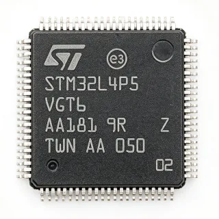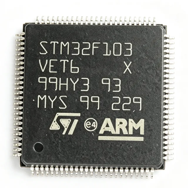
STM32F103VET6 - 512KB Flash 72MHz Cortex-M3 MCU | ST
MPN: STM32F103VET6 ✓ Active| Qty | Unit Price | Extended |
|---|---|---|
| 1 | $6.2 | $6.20 |
| 10 | $5.58 | $55.80 |
| 100 | $4.9 | $490.00 |
| 500 | $4.35 | $2,175.00 |
| 1,000 | $3.85 | $3,850.00 |
STM32F103VET6 Overview
A microcontroller (MCU) is a compact integrated circuit that governs a specific operation in an embedded system by combining a processor core, memory, and programmable peripherals on one chip. The STM32F103VET6 sits in the embedded processing hierarchy as: MCU -> STM32F1 series -> STM32 family of ARM Cortex-M microcontrollers -> semiconductor device. It serves as the central control unit in industrial automation, motor control, and consumer electronics.
Key features include the 72 MHz Cortex-M3 core delivering 1.25 DMIPS/MHz (Dhrystone 2.1), 512 KB Flash, 64 KB SRAM, and a rich peripheral set: three 12-bit ADCs, four general-purpose 16-bit timers plus two advanced PWM timers, and standard/advanced communication interfaces including USART, SPI, I2C, USB, CAN, and SDIO. Up to 80 GPIO lines, a DMA controller, and an RTC round out the integration.
Technically, the high-density STM32F103xE devices integrate a Nested Vectored Interrupt Controller (NVIC) for deterministic interrupt latency, zero-wait-state Flash execution with prefetch buffer at 72 MHz, SWD and JTAG debug support, and multiple low-power modes (Sleep, Stop, Standby) for battery-sensitive designs. The 2.0V to 3.6V supply range supports 3.3V systems with 5V-tolerant IOs.
Typical applications include industrial control systems, motor drives and inverters, medical instrumentation, POS/printing equipment, and IoT gateways where CAN, USB, and multiple ADC channels are required on a single chip.
For design, provide 100 nF decoupling on each VDD/VSS pair plus a 4.7 uF bulk capacitor, keep the VCAP pins per datasheet guidance, and use the NRST pin with an external reset circuit for reliable in-field programming via SWD.
This page synthesizes distributor pricing, drop-in alternatives (including GD32/CH32/APM32 cross-brand equivalents), and practical design notes not found in the STMicroelectronics datasheet.
Drop-in alternatives for STM32F103VET6 — same package, pin-to-pin compatible. Different-package parts requiring PCB rework are excluded.
Variants in this series
Same-series models that are drop-in compatible with STM32F103VET6 (same form factor and footprint) — differing in Flash Memory, Package, Core, Operating Temperature, SRAM.
Quick Comparison Tool — Select alternative parts for side-by-side comparison:
STM32F103VDT6
✅ Drop-In ⚠️ 参数待验证✓ In Stock
$7.1591 / Unit
View Datasheet →STM32F103VCT6
✅ Drop-In✓ In Stock
$2.68 / Unit
View Datasheet →GD32F103VET6
✅ Drop-In📋 Reference alternative (not in catalog)
APM32F103VET6
✅ Drop-In📋 Reference alternative (not in catalog)
CH32F103VET6
✅ Drop-In📋 Reference alternative (not in catalog)
STM32F103VET6 Maximum Ratings & Electrical Characteristics
| Core | ARM Cortex-M3, 32-bit RISC |
| Maximum Clock Frequency | 72 MHz |
| Core Performance | 1.25 DMIPS/MHz (Dhrystone 2.1) |
| Flash Memory | 512 KB (512K x 8) |
| SRAM | 64 KB |
| Supply Voltage Range | 2.0 V to 3.6 V |
| ADC Resolution | 12-bit |
| Number of ADCs | 3 |
| General-Purpose Timers | 4 x 16-bit |
| Advanced PWM Timers | 2 |
| Communication Interfaces | USART, SPI, I2C, USB, CAN, SDIO |
| GPIO Count | Up to 80 |
| Package | 100-LQFP (14x14 mm) |
| Mounting Type | Surface Mount |
| Operating Temperature | -40C to +85C |
| Debug Interfaces | SWD, JTAG |
| Series | STM32F1 (high-density performance line) |
| RoHS Status | Compliant |
STM32F103VET6 100-lqfp (14x14 mm) Pin Configuration Guide
Pin configuration for STM32F103VET6 (100-lqfp (14x14 mm) package). This digital IC includes GPIO, communication interfaces (UART, SPI, I2C), and power pins. Refer to the manufacturer datasheet for alternate pin functions and configuration options. Essential for embedded system design and PCB layout.

No detailed pinout data available for STM32F103VET6.
Refer to the datasheet for full pin configuration.
Typical Applications
STM32F103VET6 is suitable for 6 applications: Industrial Control Systems, Motor Drives and Inverters, Medical and Diagnostic Devices, IoT Gateways and Nodes, Consumer Electronics and POS Equipment, Automotive Aftermarket and Telematics (Non-Safety).
Industrial Control Systems
The STM32F103VET6 fits industrial PLC I/O modules and machine controllers because its 512 KB Flash accommodates communication stacks (Modbus, CANopen) alongside the control logic, and its three 12-bit ADCs digitize multiple analog sensor channels with resolution suitable for 0-10V industrial signals after scaling. In a typical design the MCU scans inputs on a timer interrupt at 1 kHz, executes the control loop on the 72 MHz Cortex-M3 core, and reports status over CAN or RS-485/USART. The -40C to +85C temperature rating supports cabinet-mounted equipment. Because the high-density family also offers SDIO, logged data can be written to SD cards locally. Firmware updates in the field use the built-in bootloader over USART, minimizing maintenance cost in installed bases.
Recommended
Motor Drives and Inverters
The STM32F103VET6 targets motor control through its two advanced PWM timers providing complementary outputs with programmable dead-time insertion and brake inputs - mandatory features for three-phase BLDC, PMSM, and induction drives. Its three 12-bit ADCs allow simultaneous-ish sampling of DC-bus current, phase currents, and bus voltage for field-oriented control executed at 10-20 kHz on the 72 MHz core, which delivers roughly 90 DMIPS - sufficient for sensorless FOC at moderate dynamics. The CAN interface connects the drive to higher-level automation networks, while 512 KB Flash stores parameter tables, and fieldbus protocol stacks. Designers should place current-sense filtering close to the ADC pins and use the hardware brake input for overcurrent shutdown within microseconds, independent of software latency.
Recommended
Medical and Diagnostic Devices
The STM32F103VET6 is widely used in medical instrumentation such as blood analyzers, infusion pumps, and patient-monitoring front ends. The three 12-bit ADCs, combined with a stable internal voltage reference workflow and DMA-driven sampling, digitize biosignals without loading the analog front end, while the 72 MHz Cortex-M3 core runs filtering and calibration math. 512 KB Flash holds device UI assets, calibration tables, and communication firmware simultaneously - a key reason designers choose the VE over smaller densities. USB device connectivity links to host PCs for data export, and the RTC plus backup domain maintains time-stamping across power events, important for audit logging. For designs where long-term silicon supply predictability is a regulatory concern, ST's roadmap documentation supports component lifecycle management.
Recommended
IoT Gateways and Nodes
The STM32F103VET6 serves as a bridge controller in IoT gateways, aggregating sensor data over multiple interfaces - up to five USARTs, three SPIs, two I2Cs, CAN, and SDIO - toward a radio module connected via UART or SPI. Its 64 KB SRAM buffers packet payloads while the 512 KB Flash stores a TLS-light stack and OTA update images side by side; dual-bank-style image staging can be implemented by partitioning Flash. DMA on all major peripherals offloads data movement so the 72 MHz core focuses on protocol processing. Sleep and Stop modes let battery-assisted nodes drop to microamp-level consumption between polling windows. When radio modules such as LoRa or NB-IoT transceivers are used, hardware flow control on USART plus the MCU's abundant GPIO handles module reset, boot, and status lines cleanly.
Recommended
Consumer Electronics and POS Equipment
Thermal printers, POS terminals, card readers, and small appliances use the STM32F103VET6 as the main system controller because it integrates everything a cost-sensitive product needs on one chip: USB device for PC connectivity, multiple USARTs for peripheral heads, 512 KB Flash for font tables and graphics, and 80 GPIO for keypads, indicators, and stepper drivers. The 72 MHz core renders simple UIs and drives print-head timing with timer DMA. The 3.0V to 3.3V operation matches single-cell lithium systems regulated to 3.3V, and the -40C to +85C range covers storage and transport conditions. Chinese drop-in equivalents (GD32F103VET6, APM32F103VET6) are frequently second-sourced in this segment for supply resilience, since package and code compatibility make dual-sourcing practical after validation.
Recommended
Automotive Aftermarket and Telematics (Non-Safety)
For non-safety automotive applications such as telematics boxes, fleet trackers, battery monitors, and accessory controllers, the STM32F103VET6 provides the mandatory CAN 2.0B interface for OBD-II and vehicle bus access, alongside multiple USARTs for modems and GNSS modules. Its 512 KB Flash supports J1939 stacks plus logging firmware, and the RTC with VBAT backup keeps timestamps through power loss. Operating from a 3.3V rail derived from the vehicle's 12V via a step-down regulator, the MCU's wide -40C to +85C rating meets under-dash environmental requirements. Engineers should add transient protection (TVS) on CAN lines and use the MCU's Stop mode with CAN wake-up to keep quiescent draw within battery-drain budgets during parking periods. Note this part is not AEC-Q100 qualified - restrict use to aftermarket and non-safety functions.
Recommended
Recommended Products Summary
Engineering reference data for STM32F103VET6 — comparison, design guidance, and compliance information.
Selection Guide
Comparison with Alternatives
| Parameter | This Product | STM32F103VDT6 | STM32F103VCT6 | GD32F103VET6 | APM32F103VET6 |
|---|---|---|---|---|---|
| Package | 100-LQFP (14x14 mm) | 100-LQFP (14x14 mm) - same | 100-LQFP (14x14 mm) - same | 100-LQFP (14x14 mm) - same | 100-LQFP (14x14 mm) - same |
| Brand | STMicroelectronics | STMicroelectronics | STMicroelectronics | GigaDevice | Geehy Semiconductor |
| Flash Memory | 512 KB | 384 KB | 256 KB | 512 KB | 512 KB |
| Maximum Clock | 72 MHz | 72 MHz | 72 MHz | 108 MHz | 72 MHz |
| Core | ARM Cortex-M3 | ARM Cortex-M3 | ARM Cortex-M3 | ARM Cortex-M3 | ARM Cortex-M3 |
| Supply Voltage | 2.0 V to 3.6 V | 2.0 V to 3.6 V | 2.0 V to 3.6 V | 2.6 V to 3.6 V | 2.0 V to 3.6 V |
| Ecosystem / Software | STM32Cube, HAL, RM0008 reference manual | Identical to STM32F103VET6 | Identical to STM32F103VET6 | GD32 firmware library, ST-HAL mostly portable | Geehy SDK, ST-HAL mostly portable |
Key Differentiators
- Maximum Flash density in the LQFP100 F103 family (vs STM32F103VCT6)
- Native ST ecosystem and errata transparency (vs GD32F103VET6)
- Two advanced PWM timers with dead-time and brake (vs APM32F103VET6)
Design Notes
Provide one 100 nF ceramic capacitor per VDD/VSS pair, placed within 2-3 mm of each pin pair, plus a single 4.7 uF to 10 uF bulk capacitor near the MCU. The internal 1.8 V core regulator is decoupled via the VCAP pins with the exact capacitance specified in the datasheet - do not substitute values. Estimated: at 72 MHz full-speed execution expect tens of mA core current per MCU, so size the 3.3 V regulator for total system load including GPIO output currents.
Route the 8 MHz HSE crystal with short traces, guard it with ground, and keep the 20 pF-class load capacitors close to OSC_IN/OSC_OUT. Keep the SWDIO/SWCLK debug header on the board even in production - ST's system bootloader plus SWD enables field reprogramming. VBAT should connect to the 3.3 V rail through a diode-OR with a coin cell if RTC retention through power loss is required.
Three frequent STM32F103 mistakes: (1) leaving BOOT0 floating - tie it to GND through a 10 kR resistor or the device may boot into the system bootloader; (2) driving non-FT (non-five-volt-tolerant) pins above VDD in 5 V mixed-signal designs - check the datasheet FT markers per pin; (3) assuming drop-in Chinese alternatives (GD32/APM32/CH32) work without retesting Flash wait states, HSE startup, and USB timing - always run full firmware regression on the substitute silicon.
Compliance Information
RoHS compliant and lead-free per ST ordering information (T6 suffix). REACH and conflict-minerals declarations available via ST product-page compliance documents; not AEC-Q100 qualified - for automotive safety applications use ST automotive-grade parts.