ADC/DAC
Produtos (2518)

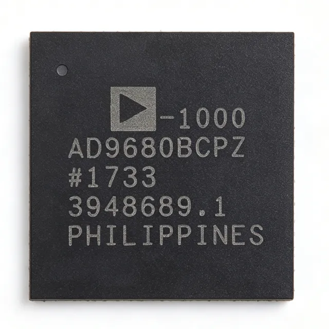
AD9680BCPZ-1000 - Dual 14-Bit 1 GSPS ADC | Analog Devices
The Analog Devices AD9680BCPZ-1000 is a dual 14-bit pipelined analog-to-digital converter with two inputs, a maximum sampling rate of 1 GSPS for this ordering option, and a 64-lead LFCSP package measuring 9 mm by 9 mm. It is designed for high-speed signal conversion with JESD204B support. The device family supports 1.25 GSPS, 1 GSPS, 820 MSPS, and 500 MSPS operating modes. An ADC converts an analog voltage into a digital code for processing, storage, transmission, or measurement. The AD9680 belongs to the high-speed ADC category, combines a pipelined conversion architecture with on-chip input buffers and sample-and-hold circuits, and is intended for communications, instrumentation, radar, and test systems. Its dual-channel architecture allows two analog inputs to be digitized while preserving matched device characteristics. Key features include 14-bit resolution, dual simultaneous input capability, and operation from a 1.2 V or 2.5 V supply domain as identified in the verified product information. The JESD204B interface enables high-rate digital data transfer between the converter and compatible serializers or processors. The integrated input buffer and sample-and-hold circuit are specifically mentioned by the manufacturer as supporting low power, small size, and ease of use. At high conversion rates, the ADC must be paired with controlled analog input networks, adequate power delivery, proper clocking, and a digital interface capable of handling the resulting data rate. The two analog channels should use matched routing and impedance considerations to reduce channel-to-channel errors. JESD204B configuration, clock relationships, lane rates, reference voltage, and supported device features must be verified in the manufacturer datasheet before board release. Typical applications include wireless infrastructure, digital oscilloscopes, spectrum analyzers, radar receivers, communications test equipment, and broadband signal-processing systems. The AD9680 is particularly relevant where multiple high-speed analog channels must be converted into data suitable for high-speed serial transport. Designers should pay particular attention to the 9 mm by 9 mm LFCSP footprint, exposed-pad thermal management, decoupling, high-speed clock routing, analog input bandwidth, and JESD204B lane configuration. The verified sources identify the component and its major conversion characteristics, but do not provide a complete verified pinout, electrical limit table, lifecycle statement, pricing schedule, or qualified drop-in substitute set. This page consolidates the verified Analog Devices product information, distributor identifiers, application guidance, and design constraints. It also separates documented facts from missing parameters so that engineers can make sourcing decisions without confusing generic ADC recommendations with verified AD9680BCPZ-1000 data.
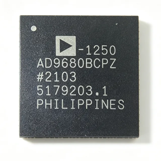
AD9680BCPZ-1250 - Dual 14-Bit 1.25 GSPS ADC JESD204B | Analog Devices
The Analog Devices AD9680BCPZ-1250 is a dual-channel, 14-bit, 1.25 GSPS pipelined analog-to-digital converter (ADC) with a JESD204B high-speed serial output interface, housed in a 64-lead LFCSP (9 mm x 9 mm) package. It is designed for sampling wide-bandwidth analog input signals of up to 2 GHz. An ADC (analog-to-digital converter) is a mixed-signal semiconductor device that converts continuous analog waveforms into discrete digital data for processing by FPGAs, DSPs, or other digital logic. Within the signal-chain hierarchy, the AD9680 belongs to the RF-sampling, high-speed pipelined ADC class, sitting upstream of digital processing elements such as the Intel/Altera and Xilinx FPGAs commonly paired with it over JESD204B serial links. Key features include dual 14-bit conversion cores running at up to 1.25 GSPS per channel, an on-chip buffer and sample-and-hold circuit optimized for low power, small size, and ease of use, and a JESD204B serial data output that dramatically reduces pin count versus parallel LVDS/CMOS interfaces. Speed-grade variants of the same family offer 500 MSPS, 820 MSPS, 1 GSPS, and 1.25 GSPS, allowing a single PCB footprint to serve multiple bandwidth tiers. Technically, the pipelined architecture uses cascaded sub-ranging stages with digital error correction, enabling high sample rates while maintaining 14-bit resolution. The integrated input buffer eases drive requirements for wideband amplifiers or passive networks, and on-chip digital functions (DDC-style processing blocks per the ADI product family) reduce FPGA resource load in digital pre-distortion and observation-receiver designs. Typical applications include wideband software-defined radios, 3G/4G/5G cellular base-station receivers, digital pre-distortion (DPD) observation channels, and test-and-measurement instrumentation requiring GHz-class analog input bandwidth. Design consideration: operate within the recommended clock and supply architecture, and budget power and thermal performance for the 64-LFCSP thermally enhanced package, since multi-gigasample operation drives the dominant portion of power dissipation. This page synthesizes distributor pricing and availability, drop-in same-family speed-grade alternatives, and practical design guidance not consolidated in the manufacturer datasheet. Pricing shown is as of 2026-09-05.
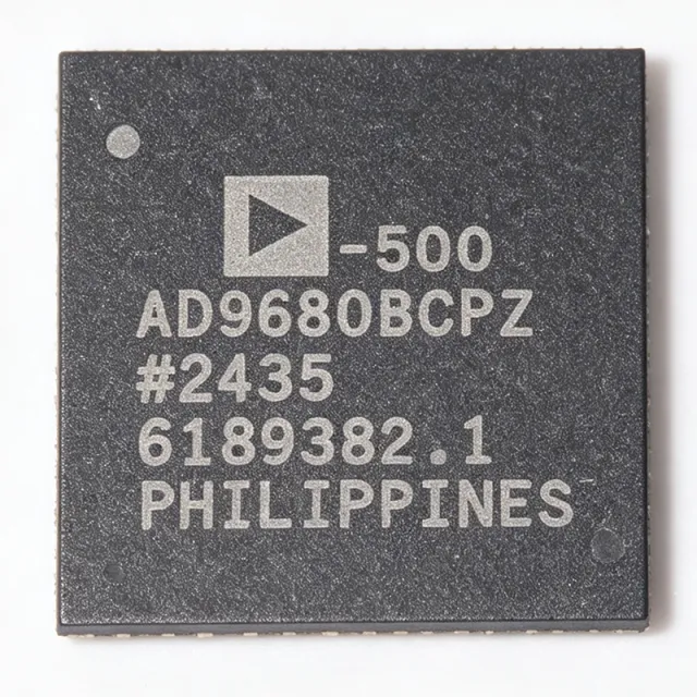
AD9680BCPZ-500 - Dual 14-Bit 500 MSPS JESD204B ADC | Analog Devices
The Analog Devices AD9680BCPZ-500 is a dual, 14-bit, 500 MSPS pipelined analog-to-digital converter (ADC) housed in a 64-lead LFCSP (9 mm x 9 mm) package with exposed pad, featuring a JESD204B serial digital output interface and 1.2 V/2.5 V dual supply operation. An analog-to-digital converter (ADC) is a mixed-signal integrated circuit that samples a continuous analog waveform and converts it into a discrete digital representation. High-speed ADCs like the AD9680 sit at the front end of the signal chain hierarchy - after amplification and filtering, and before digital processing in FPGAs or ASICs - making them critical components in any wideband data acquisition system. Key features include a 14-bit pipelined core per channel, a JESD204B high-speed serial output that drastically reduces pin count versus parallel LVDS or CMOS interfaces, an on-chip buffer and sample-and-hold circuit designed for low power, small size, and ease of use, and fast detect outputs (FD_A and FD_B on pins 17 and 32) for channel power monitoring. Architecturally, each channel uses a pipelined conversion topology in which the input is successively quantized by cascaded low-resolution stages, enabling 500 MSPS throughput while the integrated buffer relaxes external drive requirements. The multi-rail supply architecture (1.2 V core, 2.5 V analog) optimizes power consumption versus dynamic performance. Typical applications include software-defined radio and military communications receivers, wideband test and measurement instrumentation, cellular basestation receivers, and radar/electronic warfare systems where dual-channel simultaneous sampling at hundreds of megahertz is required. A key design consideration is the JESD204B link configuration and clocking architecture: a low-jitter sampling clock is essential to realize the full SNR potential of the 14-bit core, so engineers should budget jitter carefully and follow ADI reference designs for the SYSREF and device clock distribution. This page synthesizes verified distributor data, drop-in same-family alternatives, and practical engineering design guidance not found in a single manufacturer datasheet, providing a complete selection resource in one place.
AD9680BCPZRL7-1000 - Dual 14-Bit 1 GSPS ADC JESD204B | Analog Devices
The Analog Devices AD9680BCPZRL7-1000 is a dual, 14-bit, 1 GSPS analog-to-digital converter (ADC) with a JESD204B serial data output interface, supplied in a 64-lead LFCSP (9 mm x 9 mm) package with exposed pad. An analog-to-digital converter (ADC) is a mixed-signal semiconductor that samples a continuous analog waveform and quantizes it into discrete digital values. High-speed pipelined ADCs such as the AD9680 sit at the top of the data-converter hierarchy, bridging the analog front end of an RF or IF signal chain to a digital processor, FPGA, or ASIC. In modern wideband receivers, the ADC defines the system's instantaneous bandwidth, dynamic range, and noise floor, making its selection one of the most impactful decisions in a digital receiver design. Key features of the AD9680 include dual 14-bit conversion cores rated at 1.25 GSPS (with the -1000 grade specified at 1 GSPS), an on-chip buffer and sample-and-hold circuit designed for low power, small size, and ease of use, and a JESD204B high-speed serial output that dramatically reduces pin count versus parallel LVDS/CMOS interfaces. The JESD204B lane interface supports multi-lane serialization with deterministic latency, simplifying FPGA interfacing. Architecturally, the AD9680 uses a pipelined conversion architecture with on-chip references and buffering, which minimizes external analog component count. The device operates from 1.2 V and 2.5 V supplies per the datasheet title (1.2 V/2.5 V operation), supporting low overall power consumption for its class. Multiple sampling-rate grades (1.25 GSPS / 1 GSPS / 820 MSPS / 500 MSPS) share a common register map, and ADI's SPI Controller software supports the AD9680, AD9234, and AD9690, easing design migration within the family. Typical applications include wideband software-defined radio (SDR) receivers, radar and electronic warfare digitizers, test and measurement instrumentation, and multi-channel communications infrastructure where two synchronized high-dynamic-range channels are required in a compact footprint. Design considerations: the JESD204B link requires careful FPGA-side lane mapping and sysref timing design, and the exposed-pad LFCSP package demands a well-designed thermal via array under the pad for rated performance. This page synthesizes distributor availability, same-family drop-in speed-grade alternatives, and practical design notes not found in the manufacturer datasheet alone. Pricing, where listed, is referenced as of 2026-09-05.

AD974AN - 16-Bit 4-Channel 200kSPS ADC | Analog Devices
The Analog Devices AD974AN is a four-channel, 16-bit, 200 ksps data acquisition system with a serial interface, housed in a 28-pin DIP package. It combines a four-channel input multiplexer, a successive-approximation switched-capacitor ADC, and a +2.5 V internal reference on a single chip. The device operates from one +5 V supply, supports power-down operation, and accepts analog input ranges of 0 V to +4 V, 0 V to +5 V, or ±10 V. An ADC is an analog-to-digital converter, a semiconductor that transforms continuous analog voltage signals into digital codes for processing, measurement, or transmission. The AD974 belongs to the ADC hierarchy within data-conversion ICs and power-management-dependent signal-chain components. Its four-channel multiplexer allows one 16-bit ADC core to sample multiple analog inputs sequentially, reducing board area while preserving simultaneous data-acquisition capability. Key features include 16-bit resolution, four multiplexed analog inputs, a 200 ksps conversion rate, a serial data interface, and a +2.5 V internal reference. The single +5 V supply simplifies system power architecture. Supported input ranges include 0 V to +4 V, 0 V to +5 V, and ±10 V, enabling the same converter family to serve unipolar industrial, instrumentation, and bipolar measurement systems. The AD974 uses a successive-approximation, switched-capacitor conversion architecture. This architecture is appropriate for high-resolution, moderate-speed acquisition where a serial output is sufficient and per-channel simultaneous converters would add unnecessary cost and board space. The internal +2.5 V reference supports repeatable conversion behavior without requiring a separate reference circuit, although system accuracy still depends on appropriate analog conditioning, layout, and input-range configuration. Typical applications include industrial process monitoring, sensor acquisition, laboratory measurement equipment, data logging, and embedded instrumentation. The 200 ksps sampling rate is well suited to continuously updated measurements, while 16-bit resolution supports applications requiring more detail than typical 8-bit or 12-bit converters. The four-channel input structure is particularly useful when several related signals must be scanned through a shared ADC. Designers should account for input settling time, source impedance, reference accuracy, analog noise, and the sampling interval between multiplexed channels. Place input conditioning and decoupling close to the device, preserve clean grounding around the analog pins, and verify the configured input range against the source voltage. System-level error budget should also include multiplexer transition time and any external amplifier or sensor limitations.

AD974AR - 4-Channel 16-Bit 200kSPS ADC | Analog Devices
The Analog Devices AD974AR is a 4-channel, 16-bit, 200 kSPS data acquisition system with a serial interface, housed in a 28-pin SOIC package. It operates from a single 5 V supply and integrates a four-channel input multiplexer, a successive-approximation switched-capacitor ADC, a 2.5 V internal reference, and a high-speed serial interface. Supported analog input ranges include 0 V to +4 V, 0 V to +5 V, and ±10 V. A data acquisition system combines analog signal conditioning, multiplexing, sampling, quantization, and digital conversion into one integrated device. The AD974AR belongs to the ADC family within data-converter and signal-processing semiconductors. Its four-channel multiplexer reduces the need for separate analog switches when several sensors or measurement nodes must be digitized with one converter. The main features are 16-bit resolution, 200 kSPS conversion throughput, four analog input channels, a 2.5 V internal reference, and a single 5 V supply. A power-down mode reduces consumption when acquisition is not required. The serial interface allows converted samples to be transferred efficiently to a digital controller, while the successive-approximation switched-capacitor architecture supports a practical balance among speed, resolution, power, and implementation complexity. The AD974AR can accommodate 0 V to +4 V, 0 V to +5 V, or ±10 V analog input ranges. These ranges make the converter applicable to unipolar industrial measurements, positive voltage sensing, and bipolar instrumentation. The exact input bandwidth, acquisition time, conversion timing, output logic levels, reference accuracy, and operating-temperature limits are not supplied in the verified excerpts and must be confirmed in the manufacturer datasheet before design release. Typical uses include industrial process monitoring, multichannel sensor acquisition, laboratory instrumentation, control systems, and embedded measurement platforms. In each case, the four-channel multiplexer is valuable when multiple signals must share one ADC. Designers should account for source impedance, sampling-charge requirements, serial-interface timing, analog grounding, and the selected input range rather than treating the converter as a direct voltage-measurement block. For reliable operation, place input and reference components close to their associated pins, provide a clean 5 V supply, and route high-speed serial signals away from sensitive analog inputs. Confirm pin functions, package details, acquisition timing, and electrical limits against the official AD974 datasheet. This page combines the verified product description, distributor availability information, package identity, and engineering guidance for legacy or redesign scenarios.
AD974BN - 4-Channel 16-Bit 200 kSPS ADC | Analog Devices
The Analog Devices AD974BN is a four-channel, 16-bit, 200 kSPS data acquisition system with a serial interface, packaged in a 28-pin PDIP. It integrates a four-channel input multiplexer, a high-speed successive-approximation switched-capacitor ADC, a +2.5 V reference, and a single +5 V supply. The supported analog input ranges are 0 V to +4 V, 0 V to +5 V, and ±10 V. An ADC converts continuously varying analog signals into numeric values for measurement, control, or signal processing. The AD974BN combines four single-ended analog inputs with a common 16-bit conversion engine, making it useful when several sensors or voltage signals must be sampled by a compact system. Its serial interface reduces the number of parallel data lines needed on the PCB and supports communication with a digital controller. The converter provides 16-bit nominal resolution and 200 kSPS throughput. These figures define the balance between measurement detail and acquisition speed: the device samples up to 200,000 times per second while representing each selected channel with 16-bit digital data. The integrated reference is +2.5 V, and the system operates from a single +5 V supply. A power-down mode is also included for applications that need to reduce consumption when conversion is not required. The AD974 architecture uses a four-channel input multiplexer and a successive-approximation switched-capacitor conversion process. The input multiplexer selects one of four single-ended analog channels for conversion, while the serial interface transfers conversion results. The integrated 2.5 V reference provides a defined internal reference option, and the datasheet states that the device supports either external or internal reference selection. Typical applications include industrial process monitoring, sensor signal acquisition, laboratory instrumentation, communications equipment, and embedded measurement systems. The four-channel structure is useful when monitoring multiple voltages sequentially, while the 200 kSPS rate supports measurements where moderate-to-high sampling throughput is needed without requiring a parallel ADC output interface. When designing around the AD974BN, preserve adequate analog and digital return paths, place input-conditioning components close to the relevant pins, and account for the selected input range when defining signal scaling. The serial interface timing and power-down behavior should be checked against the controller requirements in the Analog Devices AD974 datasheet.
AD974BR - 4-Channel 16-Bit 200kSPS ADC | Analog Devices
The Analog Devices AD974BR is a four-channel, 16-bit, 200 kSPS data acquisition system with a high-speed serial interface, packaged in a 28-pin SOIC. It combines a four-channel analog input multiplexer, a successive-approximation switched-capacitor ADC, a +2.5 V internal reference, and an on-chip clock. The converter operates from a single +5 V supply and supports 0 V to +4 V, 0 V to +5 V, and ±10 V analog input ranges. Its 200 kSPS throughput and 16-bit resolution make it suitable for precision signal acquisition, industrial measurement, instrumentation, and embedded control systems where multiple analog channels must be digitized with limited board space. A data acquisition system combines analog multiplexing, sampling, quantization, conversion, and a digital interface into one integrated device. This integration reduces the number of external components and simplifies synchronization between analog channels. The AD974BR is a low-power ADC/data acquisition IC within the broader semiconductor hierarchy: data acquisition system → analog-to-digital converter → ADC/DAC component. Its internal reference and on-chip clock are particularly useful when a system requires repeatable conversions without relying on separate reference and timing components. The principal features are a 16-bit conversion resolution, 200 kSPS throughput, four single-ended analog input channels, and a single +5 V supply. The device accommodates several input ranges, including 0 V to +4 V, 0 V to +5 V, and ±10 V. A power-down mode helps reduce consumption when acquisition is not required, while the serial interface supports integration with digital controllers. The manufacturer describes the AD974 as a low-power data acquisition system, and the verified product information identifies a maximum power dissipation of 120 mW. The AD974 uses a successive-approximation switched-capacitor conversion architecture. This architecture is appropriate for acquisition systems that need deterministic sampling, compact implementation, and direct digital output without a complex high-frequency pipeline. The four-channel multiplexer allows one ADC core to process multiple analog inputs sequentially. The serial interface is useful when the converter is connected to a microcontroller, DSP, programmable controller, or other data-processing device; however, the exact supported clock, framing, and output timing must be confirmed from the manufacturer datasheet before final interface design. Typical applications include industrial process monitoring, laboratory instrumentation, sensor-interface systems, factory automation, medical instrumentation, and embedded measurement platforms. The four-channel structure is useful when several analog sensors or conditioned signals must be scanned through one converter. The 200 kSPS sampling rate supports applications requiring periodic measurement rather than high-bandwidth waveform capture. The 16-bit format provides fine numerical resolution for control loops and measurement systems, while the single +5 V supply simplifies power architecture. Designers should confirm the package pinout, analog input configuration, reference selection, clock requirements, and serial-interface timing from the AD974 datasheet. Input conditioning, filtering, grounding, and protection must be selected for the intended voltage range. The SOIC package also requires attention to thermal dissipation and copper routing, particularly when the converter operates continuously at its maximum sampling rate. This page combines verified Analog Devices product information, distributor listing details, package data, and practical acquisition-system guidance. It distinguishes documented parameters from information that still requires datasheet confirmation, helping engineers evaluate the AD974BR for precision multichannel measurement without relying on unverified specifications.

AD9751ASTZ - 10-Bit 300 MSPS TxDAC+ DAC | Analog Devices
The AD9751ASTZ is a dual muxed port, ultra high-speed, single-channel, 10-bit CMOS digital-to-analog converter (DAC) from Analog Devices. It integrates a high-quality 10-bit TxDAC+ core, a voltage reference, and digital interface circuitry into a compact 48-lead LQFP (7x7 mm) package. The device supports update rates up to 300 MSPS, making it suitable for high-speed waveform generation, direct digital synthesis (DDS), and communications applications. A digital-to-analog converter (DAC) is an electronic component that converts digital binary data into an analog voltage or current signal. DACs are essential in systems where digital processing must interface with the analog world, such as audio playback, video rendering, and RF signal generation. The AD9751 belongs to the TxDAC+ family, a series of high-speed DACs optimized for transmit path applications in communication systems. These DACs are part of the broader data converter category, which includes ADCs and DACs, and are critical in mixed-signal processing chains. Key features of the AD9751ASTZ include a 10-bit resolution, a maximum update rate of 300 MSPS, and a dual muxed port interface that allows interleaved data input for high-speed operation. The device operates from a 3.0V to 3.6V supply, with a typical full-scale output current of 20 mA. It offers excellent AC and DC performance, including a spurious-free dynamic range (SFDR) of 68 dBc at 10 MHz output, and a low glitch energy of 5 pV-s. The integrated voltage reference simplifies design, while the 48-lead LQFP package provides a compact footprint for space-constrained applications. Technically, the AD9751 uses a segmented current-steering architecture, which balances speed and linearity. The dual muxed port allows the DAC to accept data from two parallel input ports, effectively doubling the data throughput. The device includes a clock input that latches data on the rising edge, and it supports both binary and two's complement input formats. The output is a differential current, which can be converted to a voltage using an external resistor or transformer. The device also features a power-down mode to reduce consumption when idle. Typical applications include base station transmit paths, arbitrary waveform generators, and high-speed instrumentation. In a base station, the AD9751 converts digital baseband signals to analog IF signals for upconversion. Its high update rate and low noise make it ideal for generating clean, wideband signals. In test equipment, it enables precise waveform synthesis for signal generation and modulation analysis. When designing with the AD9751ASTZ, ensure proper decoupling of the analog and digital supply pins, and use a low-jitter clock source to maximize SFDR. The output current should be terminated with a 50-ohm load or transformer to achieve optimal performance.
AD9751ASTZRL - 10-Bit 300 MSPS TxDAC+ DAC | Analog Devices
The AD9751ASTZRL is a dual muxed port, ultra high-speed, single-channel, 10-bit CMOS digital-to-analog converter (DAC) from Analog Devices. It integrates a high-quality 10-bit TxDAC+ core, a voltage reference, and digital interface circuitry into a compact 48-lead LQFP package. The device supports output update rates up to 300 MSPS, making it suitable for high-speed communication and signal synthesis applications. A digital-to-analog converter (DAC) is an electronic component that converts digital binary data into an analog voltage or current signal. DACs are essential in systems where digital processing must interface with the analog world, such as in transmitters, waveform generators, and audio equipment. The AD9751 belongs to the TxDAC+ family, which is optimized for high-speed, high-performance transmit paths in communication systems. Key features of the AD9751 include excellent spurious-free dynamic range (SFDR) and intermodulation distortion (IMD) performance, with SFDR to Nyquist at 25 MHz output of 64 dB. It also features an internal clock doubling PLL, differential current outputs, and a flexible digital interface. The device operates from a single 3.3V supply and includes a power-down mode for reduced power consumption. The AD9751 uses a segmented current-source architecture to achieve high linearity and low glitch energy. The dual muxed port architecture allows interleaving of data from two input ports, effectively doubling the data throughput. The internal PLL can double the input clock, simplifying system clocking. The device is specified over the industrial temperature range of -40°C to +85°C. Typical applications include base stations, wireless local loop, digital radio links, direct digital synthesis (DDS), and arbitrary waveform generation. The high update rate and excellent dynamic performance make it ideal for generating complex modulated waveforms in communication transmitters. When designing with the AD9751, careful attention to PCB layout is required to minimize parasitic capacitance and inductance, especially on the high-speed digital inputs and analog outputs. Proper decoupling of the analog and digital supplies is essential to achieve the specified dynamic performance.

AD9768JQ - 8-Bit 100 MSPS ECL DAC | Analog Devices
The Analog Devices AD9768JQ is an 8-bit, current-output digital-to-analog converter operating at update rates up to 100 MSPS and packaged in an 18-pin CERDIP. It accepts ECL-level digital inputs and can also operate as a two-quadrant multiplying DAC with multiplying bandwidth up to 40 MHz. The verified source reports a 5 ns digital input characteristic and a starting distributor price of $15.2202 as of 2026-10-23. A DAC is a data-acquisition and signal-generation component that converts parallel digital codes into proportional current or voltage. The AD9768 belongs to the converter hierarchy: digital-to-analog converter, current-output DAC, data converter, and semiconductor IC. Its current-output architecture is useful when the downstream circuit requires a high-speed current-to-voltage conversion stage or direct current-domain signal processing. The AD9768 provides 8-bit resolution and supports update rates as high as 100 MSPS. Its ECL-level digital interface is designed for high-speed systems, while the multiplying capability allows the DAC to be used in signal-generation, modulation, waveform-shaping, and feedback applications. The low-glitch architecture highlighted by the manufacturer is relevant to reducing unwanted transient energy during digital-code transitions, although exact glitch specifications require the complete AD9768 datasheet. Typical circuit use places the converter between an 8-bit digital source and a current-to-voltage or load network. Because the output is current-based, external analog circuitry, impedance matching, and careful grounding strongly influence signal quality. The manufacturer describes operation as a standard DAC or as a two-quadrant multiplying DAC, giving designers flexibility for both ordinary waveform generation and multiplier-style signal paths. When designing a board around the AD9768JQ, verify the exact pinout, supply requirements, input logic levels, output compliance, and timing margins from the AD9768 datasheet. The 18-pin CERDIP package is not interchangeable with a surface-mount DAC without a deliberate PCB redesign. The verified distributor result identifies the package as 18-CERDIP, while other electrical values not present in the supplied data are intentionally not guessed.
AD976ABN - 16-Bit 200kSPS SAR ADC, 5V, 28-PDIP | Analog Devices
The Analog Devices AD976ABN is a 16-bit, 200 kSPS successive-approximation analog-to-digital converter housed in a 28-pin PDIP through-hole package, designed for high-speed, low-power data acquisition on a single 5 V supply. Headline specifications include 200 kSPS throughput (the AD976 without the "A" suffix is 100 kSPS), 100 mW maximum power dissipation, and an internal 2.5 V reference that can be overridden with an external source for ratiometric or precision systems. The part contains a successive-approximation switched-capacitor ADC core with self-calibration logic, an on-chip clock, a high-speed parallel interface, and a choice of internal or external reference operation. What is a SAR ADC? A successive-approximation-register analog-to-digital converter is a sampling converter that uses a binary-search algorithm against an internal DAC and comparator to resolve one bit per clock cycle. SAR ADCs sit at the intersection of precision (16-bit and higher) and moderate speed (tens of kSPS to a few MSPS), outperforming flash and pipelined converters in power efficiency and latency while trading off raw speed. They are widely used in industrial process control, instrumentation, and data-acquisition boards where dc-to-audio bandwidth signals must be digitized without the pipeline delay of a pipelined ADC. Key features include single 5 V supply operation, 100 mW max power dissipation, internal 2.5 V reference (with external override), on-chip clock generator, factory-calibrated linearity (no user calibration required), and a high-speed parallel interface for direct connection to microprocessors, FPGAs, or DSP data buses. Input ranges are configured for unipolar 0-5 V or bipolar ±10 V operation with the proper front-end scaling. The 200 kSPS throughput of the AD976A is double the AD976 100 kSPS rate, making it the preferred choice where the bus and downstream logic can sustain the higher sample rate. Architecturally, the AD976ABN is built on a BiCMOS process that combines bipolar precision devices for the input front-end and reference buffer with CMOS logic for the SAR engine, clock, and digital interface. The switched-capacitor input architecture provides inherent sample-and-hold operation, simplifying front-end driver design. Factory calibration trims integral and differential nonlinearity to datasheet limits, removing the iterative software-calibration routine required by many older 16-bit SAR parts and accelerating design-in. Typical applications include industrial process control front ends, multi-channel data-acquisition boards, weigh-scale and strain-gauge instrumentation, motor-control current-sense digitizers, and portable test instruments that need a proven 16-bit ADC on a single 5 V rail. The high throughput and parallel interface make it well suited to closed-loop control where deterministic conversion latency is essential. Design consideration: the input driver amplifier must settle the switched-capacitor input within the acquisition window at full throughput, and the parallel interface traces should be length-matched and series-terminated to avoid digital bus coupling into the analog input. A 100 nF ceramic decoupling cap must be placed within a few millimeters of the supply pins, with bulk capacitance at the regulator output. This page synthesizes distributor pricing, drop-in alternatives, and practical design notes that complement but do not replace the Analog Devices datasheet.
AD976AN - 16-Bit 100 kSPS ADC | Analog Devices | Signal Acquisition
The Analog Devices AD976AN is a high-speed, low-power 16-bit successive-approximation analog-to-digital converter with a 100 kSPS throughput rate, single 5 V supply operation, and a 28-pin PDIP package. It accepts an analog full-scale input range of ±10 V, includes an internal 2.5 V reference, and provides a high-speed parallel interface. An ADC is a data-acquisition semiconductor that converts an analog voltage into a digital code. The AD976 family uses a switched-capacitor SAR architecture, combining high sampling throughput with factory calibration intended to minimize linearity errors. Its role in the broader hierarchy is ADC > data converter > data-acquisition IC > semiconductor. The AD976A family supports 200 kSPS throughput, while the AD976 supports 100 kSPS throughput. The verified product-page search result identifies the AD976 as a 16-bit converter and confirms the 100 kSPS rate. Other verified features include single 5 V operation, ±10 V input range, internal or external 2.5 V reference selection, an on-chip clock, and a parallel output interface. Because the AD976AN is supplied in a 28-pin PDIP package, it is primarily suited to through-hole legacy, industrial, instrumentation, and educational designs rather than compact surface-mount assemblies. Its parallel bus can require 16 data traces plus control and interface signals, making board routing and input conditioning important design considerations. Typical applications include industrial process measurement, laboratory data-acquisition systems, instrumentation amplifiers, waveform capture, and legacy control equipment. The ±10 V input range can simplify interfacing with suitable sensor and amplifier stages, while the internal reference helps reduce external component count when sufficient accuracy is available. When selecting this part, verify the complete AD976AN datasheet, pinout, timing requirements, reference configuration, input bandwidth, and acquisition timing before layout. This page synthesizes the verified manufacturer information, distributor listing, package data, and design considerations for engineers evaluating the AD976AN.
AD976ANZ - 16-Bit 100kSPS SAR ADC | Analog Devices | 28-PDIP
The Analog Devices AD976ANZ is a 16-bit, 100 kSPS successive-approximation-register (SAR) analog-to-digital converter housed in a 28-pin PDIP (N-28) through-hole package, operating from a single 5 V supply. The device delivers 16-bit resolution with a single-ended analog input and a parallel digital interface, drawing approximately 100 mW of maximum power. The BiCMOS switched-capacitor architecture provides a wide input range and excellent AC/DC performance for industrial data-acquisition systems. An SAR ADC is a successive-approximation-register analog-to-digital converter that uses a binary search algorithm against an internal precision DAC to resolve N bits in N clock steps. SAR ADCs are a subtype of Nyquist-rate data converters that sit within the broader data acquisition IC category, which itself is part of the signal-chain and mixed-signal semiconductor hierarchy. Compared to delta-sigma ADCs, SAR converters offer lower latency, deterministic throughput, and no pipeline delay, which makes them preferable for multiplexed multi-channel acquisition and event-triggered sampling. Key features include 100 kSPS guaranteed throughput, single 5 V supply operation, internal 2.5 V reference (with external reference override), and analog input range of ±10 V when using proper input scaling. The AD976ANZ integrates a high-speed parallel interface that directly connects to 16-bit microprocessors and DSPs, and includes flexible analog input conditioning for unipolar (0 V to 5 V or 0 V to 10 V) and bipolar (±5 V or ±10 V) ranges using a single +5 V supply. Throughput latency is negligible, which is critical for closed-loop control and multiplexed systems. From an architecture standpoint, the AD976 and its higher-speed sibling AD976A share Analog Devices' proprietary BiCMOS process, combining bipolar precision devices with CMOS logic for low power and high accuracy. The device is offered in three pin-compatible packages - skinny 28-pin PDIP (this AD976ANZ variant), 28-pin SOIC, and 28-pin SSOP - giving designers flexibility for prototyping, volume production, or surface-mount reflow. Typical applications include industrial process control, multi-channel data acquisition boards, instrumentation front-ends, and medical monitoring equipment. The 100 kSPS throughput is well matched to multiplexed analog input cards that sequentially sample multiple 12- or 16-bit channels. The wide analog input range also suits vibration, strain, and pressure measurement systems where high common-mode rejection is needed. When designing with the AD976ANZ, place the analog input decoupling capacitor as close to the AIN pin as possible, maintain solid ground stitching between the analog and digital ground planes, and ensure the REFCAP pin is properly buffered with a 2.2 µF ceramic capacitor to minimize conversion noise. This page synthesizes distributor pricing, drop-in compatible variants, and practical PCB layout guidance not found in the manufacturer datasheet - including a same-package, same-pinout comparison against the AD976A 200 kSPS upgrade path.
AD976AR - 16-Bit 100 kSPS SAR ADC | Analog Devices
The Analog Devices AD976AR is a 16-bit successive-approximation analog-to-digital converter with a 100 kSPS throughput rate, one single-ended input, and a 28-lead SOIC package. It operates from one 5 V supply, supports internal or external reference selection, includes an on-chip clock, and provides a high-speed parallel output interface. These characteristics make it a compact mixed-signal conversion component for industrial control, instrumentation, signal acquisition, communications, and embedded measurement systems. An ADC is an analog-to-digital converter, a semiconductor that transforms a continuous analog voltage into a numeric code. The AD976AR belongs to the successive-approximation, or SAR, ADC family. Unlike a pipeline ADC, a SAR ADC compares the sampled input against successive trial thresholds during a sequence of conversion cycles. Its sampled input, bit resolution, throughput, reference method, and parallel interface determine the balance between measurement speed, signal detail, circuit complexity, and downstream data handling. The AD976 family combines several conversion functions in one device. Its 16-bit resolution provides 65,536 possible code levels, while the AD976 version in this MPN operates at 100 kSPS. The AD976A family member reaches 200 kSPS, but it is not an interchangeable speed upgrade unless its complete pinout, timing, reference, and interface requirements are independently verified. Operation from a single 5 V supply simplifies system power planning, while internal or external reference choices support different accuracy and calibration strategies. The converter uses a switched-capperitor SAR architecture implemented with Analog Devices BiCMOS technology, combining bipolar and CMOS devices. Its internal 2.5 V reference can provide a self-contained conversion solution, while the external-reference option permits board-level reference selection. The high-speed parallel interface presents converted codes directly across digital output pins, making it suitable for logic devices, DSPs, microprocessors, or data latches capable of capturing the required output timing. Typical uses include closed-loop industrial process monitoring, low-frequency sensor digitization, laboratory measurement equipment, communications receivers, and embedded control systems. The 100 kSPS rate is appropriate for signals that do not require video-bandwidth conversion, while the 16-bit code width can preserve fine amplitude detail. Designers should verify input range, acquisition time, digital timing, output coding, reference requirements, and electrical limits against the manufacturer documentation before fixing the system architecture. A key design consideration is the relationship between sampling, acquisition, conversion, and output timing. The system must provide a stable input during the sample-and-hold interval and capture the parallel output according to the converter timing. The selected reference must satisfy the required accuracy, noise, temperature, and startup behavior, while external decoupling and grounding should follow the datasheet recommendations. This product record combines the verified manufacturer and distributor details with application guidance, design cautions, and a transparent distinction between verified specifications and unavailable data. It is intended to support initial engineering selection while avoiding unsupported assumptions about parameters, compliance, lifecycle guarantees, or replacement parts.
AD976BN - 16-Bit 100kSPS ADC | Analog Devices | 28-PDIP
The Analog Devices AD976BN is a 16-bit, 100 kSPS successive-approximation register (SAR) analog-to-digital converter operating from a single 5 V supply, housed in a 28-pin PDIP (skinny DIP) through-hole package. The part integrates a switched-capacitor SAR ADC core, an internal 2.5 V reference (selectable as external via the REF pin), and a high-speed parallel data interface with byte- and word-mode access, plus a single-ended analog input with input range up to ±10 V (with proper input scaling) or 0-4 V unipolar in default configuration. Background. A SAR ADC (successive-approximation register analog-to-digital converter) is a class of Nyquist-rate data converter that resolves one bit per internal clock cycle by comparing the sampled input against a binary-weighted internal DAC. SAR ADCs are valued for their deterministic latency, no-pipeline-delay sampling, and excellent DC linearity, making them a workhorse for industrial process control, instrumentation, and precision data acquisition. The AD976 family sits at the upper end of ADI's legacy 16-bit SAR portfolio and uses BiCMOS process technology that combines low-noise CMOS analog with bipolar drive for the internal reference and high-speed parallel bus. Key features include 100 kSPS throughput (the AD976A variant in the same family runs at 200 kSPS), 100 mW typical power dissipation from a single +5 V analog supply, internal 2.5 V reference with external override, a high-speed parallel interface configurable as 8-bit (byte mode) or 16-bit (word mode), on-chip clock, and selectable bipolar/unipolar analog input ranges. The bipolar BiCMOS process delivers low analog input current and excellent integral non-linearity (INL), suitable for precision measurement. Typical applications include industrial process control and instrumentation, data acquisition boards for legacy backplanes, medical instrumentation interfaces, and bench-top test equipment where deterministic SAR latency is preferred over pipelined ADCs. The single 5 V supply and parallel interface make it particularly well-suited for retrofits of older +5 V-only designs. When designing with this part, ensure the analog input is buffered by a low-impedance, low-noise op-amp (such as the AD845 or AD797 family) because the SAR's switched-capacitor input presents a transient kick-back at every conversion cycle. Decouple AVDD and DVDD separately, and place a 10 µF tantalum in parallel with a 0.1 µF ceramic adjacent to each supply pin. This page synthesizes current distributor pricing, drop-in 28-PDIP alternatives, application notes and PCB layout guidance not collected in any single source, so an engineer evaluating the AD976BN can make a sourcing and design decision in one pass.
AD976BR - 16-Bit 100 kSPS ADC | Analog Devices
The Analog Devices AD976BR is a 16-bit successive-approximation analog-to-digital converter with a 100 kSPS throughput rate, a single 5 V supply, and a 28-lead SOIC package. It provides one analog input, an internal 2.5 V reference option, a high-speed parallel interface, and an on-chip clock. The AD976 family is positioned for precision signal acquisition where 16-bit resolution and moderate conversion speed are required. The AD976A, in contrast, is identified in the manufacturer material as the 200 kSPS member of the same AD976/AD976A family. An ADC is an analog-to-digital converter, a semiconductor that transforms a continuously varying analog voltage into a numeric code. Within the broader hierarchy, an ADC is a data-acquisition and signal-conversion IC; a successive-approximation ADC performs conversion by comparing the input voltage with an internally generated DAC and successive trial bit decisions. This architecture provides a practical balance between conversion throughput, resolution, power consumption, and implementation complexity for industrial, communications, instrumentation, and embedded control systems. Key verified features of the AD976BR include 16-bit resolution, 100 kSPS throughput, one analog input, single 5 V operation, selectable external or internal 2.5 V reference, an on-chip clock, a high-speed parallel interface, and a maximum input range stated in the retrieved data as 100 mV. The manufacturer material also identifies low-power operation and both external and internal reference choices. The 28-lead SOIC package is confirmed by distributor and comparison listings. The AD976BR uses a switched-capacitor successive-approximation architecture. During conversion, the internal sample-and-hold network captures the input, while the comparison and DAC network determine successive code bits. Because the converter uses a parallel interface, the host system must capture or latch the 16-bit result and handle the associated digital timing. The AD976BR is therefore most useful when moderate sampling rates are sufficient but software-based or low-speed serial conversion would be inadequate. Typical applications include industrial process monitoring, sensor-interface systems, communications equipment, data-acquisition instruments, and embedded measurement platforms. The 100 kSPS rate is suitable for acquiring slowly changing or burst-sampled signals, while the 16-bit code width supports precision measurement and control. The single-supply architecture can simplify system design when a 5 V analog rail is already available, although input conditioning, reference stability, digital grounding, and timing remain important engineering concerns. When designing around the AD976BR, place input, reference, and decoupling connections according to the manufacturer datasheet and keep the analog input path away from high-current digital switching nodes. Check acquisition time, input impedance, source drive capability, reference configuration, and the host parallel-interface timing. Do not substitute a converter merely because its resolution matches; pin compatibility, sampling architecture, input range, reference behavior, and acquisition timing must also be verified. This page combines verified Analog Devices product information, distributor package and interface details, application guidance, comparison fields, and design notes. It also explicitly identifies where pricing, pinout, lifecycle, or replacement data are not present in the supplied web evidence.

AD976CN - 16-Bit 100 kSPS BiCMOS ADC | Analog Devices
The Analog Devices AD976CN is a 16-bit, 100 kSPS successive-approximation BiCMOS analog-to-digital converter operating from a single 5 V supply and housed in a 28-lead ceramic DIP package. The converter accepts one single-ended input and uses a high-speed parallel interface for direct digital data transfer. Its family supports selectable external or internal 2.5 V references and includes an on-chip clock. An ADC is an analog-to-digital converter, a data-acquisition IC that transforms a continuously varying voltage into a numeric code for processing, storage, or control. The AD976 belongs to the successive-approximation ADC hierarchy within integrated circuits and data-conversion semiconductors. At 100 kSPS and 16-bit resolution, it balances conversion speed with precision while preserving a straightforward parallel-output architecture. The AD976CN's headline parameters are its 16-bit resolution, 100 kSPS conversion throughput, and single 5 V supply operation. According to the Analog Devices AD976 product page, the closely related AD976A reaches 200 kSPS, while the AD976 is specifically identified as the 100 kSPS member. The family also supports external or internal 2.5 V references, a feature that gives designers flexibility in establishing full-scale conversion range. The BiCMOS implementation combines bipolar and CMOS process characteristics to support precision sampling, comparison, and digital output functions. Maximum power dissipation is listed as 100 mW, while typical power-supply current is specified at 14 mA under stated conditions. The converter uses a parallel data interface, which can simplify connection to older digital buses and dedicated data-acquisition controllers when timing and bus-width constraints are managed correctly. Typical uses include industrial process monitoring, instrumentation, digital measurement equipment, waveform acquisition, and embedded control systems. Its single-ended input architecture is useful when the source can be referenced and scaled to the selected input range. The internal or external 2.5 V reference choice also makes the ADC suitable for laboratory and industrial systems where traceability or system-level reference partitioning affects measurement accuracy. When designing around the AD976CN, preserve the manufacturer's recommended analog and digital grounding and decoupling arrangements, and account for acquisition, conversion, and output-update timing at the system level. The 28-lead DIP package is less common in new high-density assemblies, so designers should verify connector availability and assembly process requirements before committing the footprint. Because the verified data identifies AD976CN as obsolete or EOL, lifecycle planning and sourcing risk are significant selection considerations. This page consolidates the verified manufacturer specifications, lifecycle information, sourcing context, and design implications for AD976CN. It also distinguishes verified facts from parameters that remain unavailable in the supplied data, helping engineers evaluate legacy replacements without assuming unverified electrical or pin-level compatibility.
AD976CNZ - 16-Bit 100kSPS BiCMOS ADC | Analog Devices
The Analog Devices AD976CNZ is a 16-bit, 100 kSPS successive-approximation analog-to-digital converter in a 28-pin PDIP (N-28) through-hole package. It operates from a single 5 V supply (4.75 V to 5.25 V), accepts input ranges of ±10 V, 0-10 V, and 0-4 V, and delivers 100 mW typical power dissipation, suiting it to industrial instrumentation, data acquisition, and process control front ends. An ADC (analog-to-digital converter) is a mixed-signal integrated circuit that converts a continuous-time, continuous-amplitude analog input into a discrete-time, discrete-amplitude digital codeword. Within the broader signal-chain taxonomy, an ADC belongs to data converters, which sit alongside DACs (digital-to-analog converters) in mixed-signal ICs. Successive-approximation-register (SAR) ADCs use a binary-search algorithm and an internal precision DAC to converge on the input voltage in N clock cycles, achieving high resolution at moderate sampling rates with very low latency and zero pipeline delay. Key features include 16-bit resolution, 100 kSPS throughput, a parallel data interface, single 5 V supply operation, and an internal 2.5 V reference. The device is specified over the -40 °C to +85 °C industrial temperature range, uses a switched-capacitor input architecture, and dissipates only 100 mW maximum. The 28-pin PDIP (N-28) package simplifies prototyping and breadboarding in laboratory and factory-floor applications where socketed through-hole parts are preferred. Architecture-wise, the AD976 employs BiCMOS process technology, combining bipolar precision analog blocks with CMOS logic for the SAR engine and output latches. The BiCMOS integration reduces analog-domain noise while keeping digital control current low, supporting the part's 100 mW dissipation budget at full throughput. An external or internal reference option allows designers to trade absolute accuracy against system cost. Typical applications include industrial process control, multichannel data-acquisition systems, portable instrumentation, and PC/embedded signal-conditioning front ends. The single-5 V supply and parallel interface make it easy to interface to legacy microcontrollers, DSPs, and FPGAs without level translation. When designing with the AD976CNZ, observe the input-common-mode and acquisition-time requirements; an external input buffer amplifier is normally required to drive the switched-capacitor input. Use a low-impedance ground plane and decouple AVCC and DVCC separately to preserve the converter's 16-bit linearity. This page synthesizes distributor pricing, drop-in same-family and cross-brand equivalents, and practical design notes not found in the bare manufacturer datasheet, helping engineers source and qualify the AD976CNZ quickly.

AD977ABR - 16-Bit 200kSPS Serial SAR ADC | 20-SOIC | ADI
The Analog Devices AD977ABR is a 16-bit, 200 kSPS successive-approximation (SAR) analog-to-digital converter with a serial I/O interface, packaged in a 20-pin SOIC (R-20) wide-body surface-mount package. It operates from a single +5 V supply, dissipating a maximum of 100 mW, and supports input ranges of 0 V to 5 V (unipolar), 0 V to 4 V (unipolar), ±5 V (bipolar) and ±3.3 V (bipolar) via factory-trimmed or user-configurable scaling resistors. The SAR architecture with internal conversion clock and auto-calibrating capacitive DAC achieves true 16-bit performance with no missing codes over the industrial temperature range. An ADC (analog-to-digital converter) is a data-converter integrated circuit that samples a continuous analog input voltage and produces a corresponding digital code at its output. SAR ADCs use a binary-search successive-approximation register together with an internal DAC to resolve each conversion in N clock cycles for N-bit precision; they are valued for zero pipeline latency, deterministic behavior, low power, and excellent DC linearity. SAR converters occupy a unique position in the data-converter hierarchy between high-speed flash/pipeline ADCs (>10 MSPS) and slow integrating/sigma-delta ADCs (audio, precision DC). The AD977A family is one of the classic low-power industrial SAR ADCs of the 1990s and remains in production for installed-base applications. Key features include an aperture delay of 5 ns, track-and-hold bandwidth of 2 MHz, and a power-down mode that reduces quiescent dissipation to 50 µW for battery-powered designs. The serial interface is compatible with standard SPI/QSPI/MICROWIRE hosts, simplifying connection to microcontrollers and DSPs. Input protection diodes are absent on the analog input pin, so external clamping is required when the input can exceed the supply rails. Typical applications include industrial process control data acquisition, multichannel PLC analog input modules, portable instrumentation, weighing scales, and remote sensor digitizers. The combination of ±5 V true-bipolar input range and serial output makes the part especially well suited to legacy PLCs and 4-20 mA loop digitizers. Designers should observe the datasheet's reference decoupling and analog-input filtering guidelines to realize the rated INL/DNL and signal-to-noise ratio, and should add an external TVS/Schottky clamp at the analog input when transients beyond ±5 V are possible.

AD977ABRS - 16-Bit 200kSPS Serial I/O ADC | Analog Devices
The Analog Devices AD977ABRS is a 16-bit, 200 kSPS successive approximation register (SAR) analog-to-digital converter with a serial I/O interface, housed in a 28-pin SSOP package. Operating from a single 5 V supply, the AD977A variant delivers 200 kSPS throughput while its companion AD977 delivers 100 kSPS, both with 100 mW maximum power dissipation and a 50 µW power-down mode. An SAR ADC is a precision data converter that performs a binary search against the analog input using an internal capacitive DAC, sample-and-hold, reference, and clock. SAR ADCs occupy the precision-mid-tier in the converter hierarchy (SAR -> ADC -> data converter -> mixed-signal IC -> semiconductor), combining high DC accuracy, low latency, and a compact serial output - ideal for multiplexed data-acquisition systems. Key features of the AD977ABRS include unipolar input ranges of 0V to 5V and 0V to 4V plus bipolar ranges of ±5V and ±3.3V, providing measurement flexibility across industrial sensor signal levels. The device integrates a reference, clock, and sample-and-hold, and provides either an internal clock or an external data-clock-synchronized serial output. Maximum power dissipation is 100 mW active and 50 µW in shutdown mode. The AD977ABRS is fabricated on a BiCMOS process that pairs bipolar input buffers with CMOS logic, achieving low input-referred noise and stable DC linearity at the 200 kSPS conversion rate. The integrated 2.5 V reference and single-supply 5 V operation remove the need for external reference components in many applications. Typical applications include industrial process control, multi-channel data-acquisition systems, instrumentation, weigh scales, and portable battery-powered measurement equipment. The serial interface simplifies isolation barriers, while the small 28-SSOP footprint suits dense multi-channel layouts. When designing with this ADC, ensure the analog input is driven from a low-impedance source and referenced to AGND1 to avoid resistive ground-drop artifacts. Place the 2.5 V reference bypass and the input RC anti-alias filter within 1 mm of the input and reference pins. This page synthesizes distributor pricing, drop-in same-package alternatives, and practical design notes not found in the Analog Devices datasheet alone, enabling faster component selection and PCB layout decisions.
AD977AR - 16-Bit 100 kSPS Serial ADC | Analog Devices
The Analog Devices AD977AR is a 16-bit, 100 kSPS, single-input successive-approximation analog-to-digital converter operating from one 5 V supply and housed in a 20-pin SOIC package. The AD977 family uses a switched-capacitor ADC architecture with an internal 2.5 V reference and a high-speed serial interface. According to the Analog Devices product page, the AD977A reaches 200 kSPS while the AD977 reaches 100 kSPS. An ADC is an analog-to-digital converter, a semiconductor that samples a continuous analog voltage and produces a corresponding numeric code for digital processing. AD977AR belongs to the successive-approximation ADC family, a type commonly used where moderate sampling rate, low power, compact packaging, and straightforward system integration are more important than very high conversion bandwidth. Its 16-bit resolution supports finely quantized measurements while the single 5 V supply simplifies system power architecture. The verified features include a 16-bit conversion resolution, 100 kSPS throughput for AD977, and 200 kSPS throughput for AD977A. The device is factory calibrated, has unipolar and bipolar input-range options, supports 5 V and 3.3 V bipolar configurations as described in the retrieved datasheet material, and provides a power-down mode. Its switched-capacitor SAR architecture separates acquisition and conversion functions while retaining a compact, low-power implementation. The AD977AR is suitable for industrial measurement, instrumentation, process control, sensor acquisition, data acquisition systems, and embedded control platforms. A system designer should select the input range and reference arrangement required by the analog signal, then validate conversion timing against the 100 kSPS device rating. The serial interface reduces package pin count and board area, but the host processor must support the required clocking and data protocol. The main design consideration is analog signal conditioning. Keep the input within the selected unipolar or bipolar range, account for source impedance and sampling behavior, and provide stable reference and supply decoupling close to the device. For replacement decisions, the exact suffix, package, interface, input range, reference configuration, and timing must be checked rather than relying only on the AD977 family name. This page combines the verified AD977 family specifications with application guidance, pin-level caveats, comparison placeholders, and procurement-oriented information. It is intended to help engineers identify whether the AD977AR matches a 16-bit, 100 kSPS, single 5 V ADC design and to locate the manufacturer datasheet and distributor listings before committing to a board or production release.

AD977BN - 16-Bit 100 kSPS ADC | Analog Devices
The Analog Devices AD977BN is a 16-bit, single-channel, successive-approximation analog-to-digital converter with a 100 kSPS throughput rate, serial interface, and 20-pin PDIP package. It operates from a single 5 V supply and provides selectable unipolar and bipolar input ranges for precision signal acquisition. An ADC converts an analog voltage into a digital code for measurement, control, instrumentation, and signal-processing systems. The AD977 belongs to the successive-approximation ADC, or SAR ADC, family within the broader data-converter and mixed-signal semiconductor hierarchy. Its 16-bit resolution supports fine amplitude quantization, while its 100 kSPS throughput is suited to accurate acquisition of slowly changing or moderate-bandwidth signals. The verified product information identifies a 16-bit SAR architecture, one analog input, serial I/O, and operation from a single 5 V supply. Available input ranges include unipolar 0 V to 5 V and 0 V to 4 V, plus bipolar 0 V to 5 V and 0 V to 3.3 V. The AD977 family also offers an external-reference option, while the manufacturer describes the converter as a low-power, high-speed data-acquisition device. The AD977A is a related family member with a 200 kSPS throughput rate, whereas the AD977 used by AD977BN is specified at 100 kSPS. This distinction matters when selecting a replacement: a faster related device may require different timing, acquisition, and system-level validation even when its resolution and function are similar. Typical applications include industrial process measurement, laboratory data acquisition, instrumentation, transducer interfaces, and embedded control systems. The serial interface can reduce PCB routing requirements compared with a parallel ADC, but the host processor must read the serial data at the converter's supported rate and account for acquisition and conversion timing. For robust designs, provide a stable reference and supply, connect the analog input according to the selected input range, and validate signal-conditioning bandwidth against the 100 kSPS throughput. The 20-pin PDIP package is through-hole and is not a direct substitute for surface-mount implementations without a package and pinout review. This page combines the verified Analog Devices family description, distributor identification, package information, and practical selection guidance. It also distinguishes the AD977BN from the faster AD977A rather than presenting related family variants as interchangeable without qualification.
AD977BR - 16-Bit 100 kSPS Serial ADC | Analog Devices
The Analog Devices AD977BR is a 16-bit, 100 kSPS, single-input successive-approximation analog-to-digital converter operating from one 5 V supply in a 20-lead SOIC package. It uses serial I/O, provides unipolar and bipolar input ranges, and includes an internal 2.5 V reference according to the manufacturer product page. The converter combines a 16-bit sampling rate of 100,000 conversions per second with low-power operation and a 100 mW maximum specified power dissipation. An ADC is a data-acquisition semiconductor that converts an analog voltage into a digital code for measurement, control, instrumentation, and signal-processing systems. The AD977 belongs to the successive-approximation ADC family, also called a SAR ADC. Compared with flash and pipeline converters, a SAR ADC generally uses sequential internal comparisons, making this device suitable for moderate-speed precision acquisition where output resolution, serial communication, and low power are more important than very high conversion throughput. The AD977BR provides a 16-bit conversion result at 100 kSPS from a single 5 V supply. Its input architecture supports unipolar ranges of 0 V to 5 V and 0 V to 4 V, plus bipolar ranges of ±5 V and ±3.3 V. The verified sources also identify external-reference and power-down options, internal-reference capability, and industrial-temperature packaging. These features allow the same converter family to address sensor interfaces, process-control measurements, laboratory acquisition, and industrial diagnostic systems. The switched-capper architecture is factory calibrated, as stated in the Analog Devices datasheet description. Sampling and conversion behavior must be coordinated with the serial interface and external analog network. The AD977BR uses serial I/O rather than a parallel data bus, reducing package pin count and PCB routing requirements while requiring compatible firmware or control logic. The AD977A member provides a higher 200 kSPS rate, whereas the AD977BR is the 100 kSPS version. Typical applications include industrial process monitoring, sensor signal acquisition, medical instrumentation, laboratory measurement, communications equipment, and embedded data-acquisition systems. A system designer should verify the exact input range, reference configuration, timing, electrical limits, and pin-level requirements against the manufacturer datasheet before layout or firmware release. The most important design consideration is preserving analog signal integrity while supporting the serial interface. Keep the analog input and reference paths short, use suitable bypass and filtering components, and account for source impedance during acquisition. The verified data does not provide all timing, accuracy, temperature, and reference-load details, so those values should be obtained from the official AD977/AD977A datasheet. This page consolidates the verified manufacturer and distributor information, separates confirmed AD977BR characteristics from unknown parameters, and provides application guidance without treating unverified values as specifications.