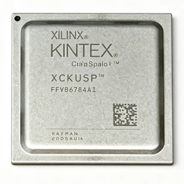
Produtos (31127)

XCKU035-2FBVA676I - Kintex UltraScale FPGA, 444K Logic Cells | AMD
XCKU035-2FBVA676I

XCKU035-2FBVA676I - Kintex UltraScale FPGA, 444K Logic Cells | AMD

The AMD XCKU035-2FBVA676I is a Kintex UltraScale Field Programmable Gate Array (FPGA) with 444,343 logic cells and 19,456,000 bits of block RAM, housed in a 676-ball Flip-Chip BGA package. Built on a 20nm process node and offered at a -2 (mid) speed grade, this device targets mid-range high-performance applications requiring an optimal balance of price, performance, and power efficiency. A Field Programmable Gate Array (FPGA) is a reconfigurable integrated circuit whose logic fabric, interconnect, and I/O can be programmed post-manufacture to implement arbitrary digital functions. FPGAs belong to the broader category of programmable logic devices (PLDs), which sit hierarchically under digital semiconductors and ICs. The Kintex UltraScale family from AMD (formerly Xilinx) addresses the spectrum between cost-optimized Artix and high-end Virtex devices, focusing on DSP, memory bandwidth, and transceiver integration. Key features of the XCKU035 include 312 maximum user I/Os, integrated DSP slices for high-throughput signal processing, dedicated block RAM (BRAM) for on-chip data storage, and high-speed serial transceivers suitable for chip-to-chip and backplane links. The device supports multiple configuration modes including JTAG, SPI, and BPI, enabling flexible boot strategies in production systems. The Kintex UltraScale architecture leverages a 20nm planar process with stacked-silicon interconnect (SSI) options in larger family members. The XCKU035 uses monolithic silicon, providing predictable performance and lower cost. The UltraScale architecture introduces enhanced routing, multi-die clocking, and improved DSP and BRAM utilization rates over prior 7-Series FPGAs. Typical applications of the XCKU035-2FBVA676I include high-speed data acquisition systems, software-defined radio (SDR) baseband processing, video broadcast equipment, industrial machine vision, 100G network interface cards, and aerospace telemetry. Its combination of logic density, memory bandwidth, and transceivers makes it well-suited for prototyping ASICs or low-volume production. When designing with the FBVA676 BGA, plan for high-density PCB fabrication with microvia or via-in-pad stackups, controlled-impedance traces for transceivers, and robust power distribution with high-frequency decoupling to satisfy simultaneous switching noise (SSN) requirements. This page synthesizes distributor pricing, FPGA drop-in alternatives within the same 676-BGA footprint, and practical design notes not typically presented in the manufacturer datasheet.

USD $52,40 Em estoque
XCKU040-2FFVA1156I - Kintex UltraScale FPGA 520 I/O | AMD
XCKU040-2FFVA1156I

XCKU040-2FFVA1156I - Kintex UltraScale FPGA 520 I/O | AMD

The AMD XCKU040-2FFVA1156I is a Kintex UltraScale FPGA with 520 user I/O, 21,606,000 system logic capacity, 530,250 DSP-equivalent resource units, speed grade -2, in a 1156-ball FCBGA package rated for industrial temperatures of -40C to +100C. A Field Programmable Gate Array (FPGA) is a semiconductor device containing a fabric of configurable logic blocks (CLBs), DSP slices, block RAM, and programmable interconnect that designers configure after manufacturing. Within the power-management hierarchy of digital system ICs, an FPGA sits at the top of the programmable logic taxonomy: programmable logic device (PLD) -> FPGA -> system-on-chip FPGA. FPGAs are used where custom logic, parallelism, or post-deployment reconfigurability is required that fixed-function ASICs or microcontrollers cannot provide. Key features of the XCKU040-2FFVA1156I include the 20nm UltraScale architecture, which lowers total power consumption versus the previous 28nm 7-series generation, a -2 speed grade for high-performance designs, and an industrial (I-suffix) temperature rating of -40C to +100C. The 1156-ball flip-chip BGA provides 520 user I/O for high-bandwidth parallel interfaces, and the fabric includes MMCM and PLL clock management resources. On the technical side, the Kintex UltraScale family focuses on price/performance using monolithic 20nm die. The device core supply operates from 0.922V to 0.979V per the datasheet listing. The UltraScale architecture adds enhanced routing, higher DSP throughput, and improved clocking compared to Kintex-7, making the XCKU040 a popular mid-density choice between the XCKU035 and XCKU060. Typical applications include industrial image processing and machine vision, wireless baseband and RF front-end processing, medical ultrasound, and ASIC prototyping. The 520 I/O count suits multi-camera sensor aggregation and high-width data converters. Design consideration: FCBGA-1156 devices require careful PCB stackup design - escape routing under the 1.0mm ball pitch typically needs via-in-pad or at least 8 layers, and core voltage rails must meet the tight 0.922-0.979V tolerance. This page synthesizes distributor pricing, drop-in alternatives, and practical design notes not found in the manufacturer datasheet.

USD $119,71 Em estoque
XCKU3P-1FFVB676E - Kintex UltraScale+ FPGA | 355K LC | AMD
XCKU3P-1FFVB676E

XCKU3P-1FFVB676E - Kintex UltraScale+ FPGA | 355K LC | AMD

The AMD Xilinx XCKU3P-1FFVB676E is a Kintex UltraScale+ field-programmable gate array (FPGA) offering 355,950 logic cells, 31,641,600 bits of block RAM, and 1,560 DSP slices, housed in a 676-ball FCBGA package (FFVB676) at the -1 speed grade and the E (extended) temperature tier. It integrates 280 user I/O pins and 24 transceivers supporting up to 16.375 Gbps, making it the mid-density workhorse of the Kintex UltraScale+ family. Kintex UltraScale+ FPGAs occupy a specific tier in AMD's programmable-logic taxonomy: below Virtex UltraScale+ for highest performance and above Artix-7/Artix UltraScale+ for cost-optimized applications. Architecturally, the UltraScale+ generation introduces a register-rich silicon fabric, 3rd-generation SSI (stacked silicon interconnect) techniques, and tightly coupled DSP/BRAM columns, delivering up to 2x the performance-per-watt versus the prior generation for DSP-intensive workloads such as 5G baseband, machine-learning inference, and high-speed instrumentation. Key features of the XCKU3P include 16.375 Gbps GTH transceivers (24 channels), 6.6 Tbps serial bandwidth per device, integrated 100G Ethernet MACs, and a system-monitoring block that tracks on-die voltage and temperature. The device supports DDR4-2400 with on-chip ECC and offers hardware-rooted security via bitstream encryption and authentication using AES-256 and RSA-2048. The 676-ball FCBGA package has a body size of 27 mm × 27 mm with a 1.0 mm ball pitch, suitable for high-density PCB designs using standard BGA assembly. Typical applications span high-performance digital signal processing, 100G Ethernet network interface cards, 4K/8K video processing pipelines, test and measurement instrumentation, software-defined radio (SDR), and radar/EW front-end processing. The combination of high-speed transceivers and abundant DSP resources makes it a strong fit for low-latency, line-rate processing in both wired and wireless infrastructure. When designing with the XCKU3P-1FFVB676E, allocate at least eight PCB layers with continuous GND planes and matched-length pairs for transceivers; the package's 1.0 mm pitch requires HDI stack-ups (microvias). The extended (E) temperature grade supports -40 °C to +100 °C junction, and designers must respect the 2.0 W/cm² package thermal envelope with adequate airflow or heatsinking for sustained workloads. Vivado Design Suite is required for implementation.

USD $990,00 Em estoque
XCKU5P-2FFVB676I - Kintex UltraScale+ FPGA 474K LC | AMD
XCKU5P-2FFVB676I

XCKU5P-2FFVB676I - Kintex UltraScale+ FPGA 474K LC | AMD

The AMD XCKU5P-2FFVB676I is a Kintex UltraScale+ Field Programmable Gate Array (FPGA) with 474,600 logic cells, 280 user I/Os, and 41,984,000 bits of block RAM, housed in a 676-ball FCBGA (FFVB676) package rated for the industrial temperature range. An FPGA is an integrated circuit that designers configure after manufacturing - hence field-programmable. FPGAs sit within the programmable logic device (PLD) family alongside CPLDs and form the heart of modern adaptive computing systems, providing arrays of programmable logic blocks, routing fabric, and I/O banks that enable highly parallel hardware acceleration. They are frequently used where ASIC cost or inflexibility cannot be justified. Key features of the XCKU5P include support for 725 MHz internal clocking, MMCM and PLL clock-management tiles, and core operation from 825 mV to 876 mV. The -2 speed grade balances maximum fabric performance against dynamic power, and the industrial rating (-40C to +100C junction) suits harsh deployments. Technically, the Kintex UltraScale+ family is built on a 16nm FinFET process delivering approximately 1.5x better performance-per-watt than the previous 20nm UltraScale generation. The device integrates high-speed serial transceivers, PCIe Gen3/4 hard blocks, and 100G Ethernet MAC capability, supporting high-bandwidth connectivity and partial reconfiguration for dynamic logic updates without system power-down. Typical applications include wired and wireless communications infrastructure, data center acceleration, video and image processing, and aerospace and defense systems where logic density plus low power are decisive. Designers should pay careful attention to power integrity: the 0.85 V typical core rail demands a clean, low-noise supply with dedicated power planes and extensive decoupling, and thermal dissipation under high utilization must be budgeted via the FCBGA thermal path. This page synthesizes distributor pricing, verified drop-in same-family alternatives, and practical design guidance not found in the manufacturer datasheet alone.

USD $1.660,00 Em estoque
XCVU9P-2FLGA2104I - Virtex UltraScale+ FPGA | AMD/Xilinx
XCVU9P-2FLGA2104I

XCVU9P-2FLGA2104I - Virtex UltraScale+ FPGA | AMD/Xilinx

The AMD XCVU9P-2FLGA2104I is a Virtex UltraScale+ FPGA delivering 416 user I/O, 3,911,680 Kb of block RAM capacity and 2,586,150 CLB flip-flops in a 2104-ball FCBGA (FLGA2104) package, with the -2I industrial speed grade rated for -40C to +100C operation. It targets high-performance digital designs that need massive parallel processing, on-chip memory, and high-speed serial connectivity. A Field Programmable Gate Array (FPGA) is a reconfigurable integrated circuit whose logic fabric, memory, and interconnect are programmed after manufacturing. Within the semiconductor hierarchy, FPGAs sit alongside ASICs and ASSPs as core system logic devices, and the Virtex UltraScale+ family is AMD Xilinx's flagship programmable logic line for leading-edge compute, networking, and aerospace systems. Key features include the 16nm FinFET UltraScale+ fabric, the -2 speed grade optimized for high clock frequencies, and 416 package I/O for wide external buses. The device's block RAM and UltraRAM resources (up to 270 Mb UltraRAM cited in application literature) support deep buffering for packet processing and machine learning pipelines. Architecturally, the Virtex UltraScale+ family combines CLB logic, DSP48E2 slices, block RAM, UltraRAM, and GTY multi-gigabit transceivers (52 package GTY channels cited for this device) on a single die, enabling deterministic, low-latency implementations such as hardware trading paths and 5G fronthaul. The 2104-ball FCBGA packaging provides the power and signal integrity required at these data rates. Typical applications include 5G wireless baseband, data center acceleration, AI inference, and low-latency financial trading, all of which exploit the fabric's parallelism and transceiver bandwidth. Industrial and aerospace systems also use the -I industrial temperature variant for extended thermal environments. Design consideration: plan power distribution and decoupling for the multiple VCCINT/VCCO rails early, and use AMD Xilinx Vivado for synthesis and implementation - the -2I speed grade files are required for correct timing closure. This page synthesizes distributor pricing, drop-in alternatives, and practical design notes not found in the manufacturer datasheet.

USD $5.931,20 Em estoque
XCZU11EG-2FFVF1517I - Zynq UltraScale+ MPSoC EG | AMD
XCZU11EG-2FFVF1517I

XCZU11EG-2FFVF1517I - Zynq UltraScale+ MPSoC EG | AMD

The AMD XCZU11EG-2FFVF1517I is a Zynq® UltraScale+™ MPSoC EG device integrating a Quad ARM® Cortex®-A53 MPCore™ processor system with a Dual ARM® Cortex®-R5 real-time processor, an ARM Mali™-400 MP2 graphics processing unit, and a large programmable FPGA fabric in a 1517-ball FCBGA (40x40 mm) package. The -2 speed grade and industrial temperature grade (I) make it suitable for high-performance embedded applications requiring both hardware flexibility and software agility. A System-on-Chip FPGA (SoC FPGA) combines a hard processor subsystem (PS) with programmable logic (PL) on a single die. This architecture enables designers to implement custom hardware accelerators, high-speed I/O interfaces, and real-time control functions in the PL while running an operating system such as Linux or VxWorks on the ARM cores in the PS. The Zynq UltraScale+ family sits at the high end of this hierarchy, offering advanced DSP engines, high-bandwidth DDR memory interfaces, and multi-gigabit transceivers that go beyond conventional FPGA or microcontroller solutions. Key features of XCZU11EG-2FFVF1517I include 653,100 programmable logic cells, 597,120 FPGA registers, and 22,124,954 bits of block RAM. The PS supports a 1.3 GHz maximum ARM Cortex-A53 clock, a 600 MHz Cortex-R5 clock, and a 533 MHz Mali-400 MP2 clock. Connectivity interfaces include CANbus, EBI/EMI, Ethernet, I²C, MMC/SD/SDIO, SPI, UART/USART, and USB OTG, allowing direct interface to a wide range of peripheral devices and system networks. The MPSoC is built on TSMC 16nm FinFET technology, enabling high logic density with manageable power dissipation. The -2 speed grade provides balanced timing performance for the programmable fabric, while the industrial temperature grade supports operation in demanding -40°C to +100°C environments. The 1517-ball FCBGA package with 40x40 mm body and 0.8 mm ball pitch enables high-density PCB routing for complex multi-rail power and high-speed serial links. Typical applications include edge AI inference at industrial sites, 5G/4G baseband processing, radar and electronic warfare systems, broadcast and professional AV equipment, medical imaging, and data center SmartNICs. Designers should note that the device requires multiple power rails (VCCINT, VCCAUX, VCCBRAM, VCCO, PS rails) and careful sequencing; the recommended power-up sequence can be found in PG201 (Zynq UltraScale+ PCB Design). Adequate decoupling capacitors and a solid power delivery network are critical to achieving reliable high-speed operation. When designing with this MPSoC, ensure that the boot mode pins are correctly configured for the desired QSPI, SD, or JTAG boot source. The PS can offload complex control tasks, while the PL implements latency-sensitive data path acceleration. Thermal management must consider both the PS and PL power consumption, and a heatsink or airflow is recommended for sustained high utilization.

Cotação Em estoque
XCZU11EG-3FFVF1517E - Zynq UltraScale+ MPSoC EG | AMD
XCZU11EG-3FFVF1517E

XCZU11EG-3FFVF1517E - Zynq UltraScale+ MPSoC EG | AMD

The AMD XCZU11EG-3FFVF1517E is a Zynq UltraScale+ MPSoC EG device, integrating a quad-core ARM Cortex-A53 application processor, dual-core ARM Cortex-R5 real-time processor, and ARM Mali-400 MP2 graphics processing unit with UltraScale+ programmable logic. This System-on-Chip (SoC) is housed in a 1517-pin FCBGA package (40x40 mm) and supports 464 user I/O pins. The device operates with a maximum logic cell count of 653K+ and features processor speeds of 600 MHz (Cortex-R5), 667 MHz (Mali-400), and 1.5 GHz (Cortex-A53). A Zynq UltraScale+ MPSoC is a heterogeneous computing platform that combines a multi-core ARM processing system (PS) with programmable logic (PL) fabric on a single die. This architecture enables designers to implement complex algorithms in hardware for high throughput while maintaining software flexibility for control and interface tasks. The EG variant targets embedded applications requiring a balance of compute performance and programmable logic density. Key features include the 653K+ logic cells, 464 I/O pins, and the high-performance 1.5 GHz Cortex-A53 cluster. The device supports a wide range of high-speed serial transceivers and memory interfaces, making it suitable for data-intensive applications. The -3 speed grade indicates the highest performance tier for this package, enabling maximum clock frequencies and throughput. The XCZU11EG-3FFVF1517E leverages TSMC's 16nm FinFET process technology, providing excellent power efficiency and performance. The UltraScale+ architecture includes advanced clocking resources, DSP slices, and block RAM, enabling efficient implementation of signal processing and AI inference workloads. The integrated ARM cores handle operating systems and application software, while the PL accelerates custom logic. Typical applications include software-defined radio, medical imaging, aerospace and defense systems, and high-end industrial automation. The device's combination of processing power and programmable logic makes it ideal for edge computing platforms that require real-time processing and flexible I/O. The 1517-FCBGA package supports dense PCB routing and high-speed signal integrity. When designing with this device, careful attention must be paid to power supply sequencing and decoupling. The multiple power rails (VCCINT, VCCAUX, VCCO, and PS rails) require proper filtering and sequencing to ensure reliable operation. The device also requires a configuration source, such as QSPI flash or SD card, for booting the processing system.

USD $990,00 Em estoque
XCZU15EG-1FFVB1156E - Zynq UltraScale+ MPSoC EG | AMD
XCZU15EG-1FFVB1156E

XCZU15EG-1FFVB1156E - Zynq UltraScale+ MPSoC EG | AMD

The AMD XCZU15EG-1FFVB1156E is a Zynq UltraScale+ MPSoC EG family device, integrating a quad-core ARM Cortex-A53 application processor, dual-core ARM Cortex-R5 real-time processor, and ARM Mali-400 MP2 graphics processing unit with programmable logic. This System-on-Chip (SoC) combines the flexibility of an FPGA with the performance of a multi-core processor, targeting high-end embedded applications. A Zynq UltraScale+ MPSoC is a heterogeneous computing platform that merges a processing system (PS) with programmable logic (PL) on a single die. The PS runs operating systems like Linux or bare-metal applications, while the PL implements custom hardware accelerators, high-speed I/O, and custom peripherals. This architecture enables designers to optimize performance, power, and cost by partitioning tasks between software and hardware. Key features include 747K+ logic cells, 328 user I/O pins, and a 1156-FCBGA (35x35 mm) package. The device operates with a nominal core voltage of 0.85V (range 0.825V to 0.876V) and supports clock speeds of 500MHz (Cortex-R5), 600MHz (Cortex-A53), and 1.2GHz (Mali-400). The '1' speed grade indicates standard performance, while the 'E' suffix denotes an extended temperature range of 0°C to +100°C. The XCZU15EG-1FFVB1156E is built on TSMC's 20nm technology, offering a balance of logic density, power efficiency, and performance. The device includes 256KB of on-chip RAM, a rich set of peripherals, and high-speed transceivers for connectivity. Its architecture supports hardware acceleration, real-time control, and advanced graphics, making it suitable for compute-intensive tasks. Typical applications include software-defined radio, medical imaging, aerospace and defense systems, and industrial automation. The combination of ARM cores and FPGA fabric allows for flexible, high-performance designs that can adapt to evolving requirements. When designing with this device, careful attention must be paid to power supply decoupling and thermal management. The 1156-FCBGA package requires a multi-layer PCB with dedicated power and ground planes. The device's power sequencing requirements must be followed to ensure reliable operation.

USD $750,00 Em estoque
XCZU15EG-2FFVB1156I - Zynq UltraScale+ MPSoC EG | AMD
XCZU15EG-2FFVB1156I

XCZU15EG-2FFVB1156I - Zynq UltraScale+ MPSoC EG | AMD

The AMD XCZU15EG-2FFVB1156I is a Zynq UltraScale+ MPSoC EG device that integrates a quad-core ARM Cortex-A53 application processor, a dual-core ARM Cortex-R5 real-time processor, and an ARM Mali-400 MP2 graphics processing unit with a 16nm FinFET+ programmable logic fabric. This System-on-Chip (SoC) is housed in a 1156-ball FCBGA package measuring 35x35 mm, offering 747K+ logic cells and supporting processor speeds of 533 MHz (Cortex-A53), 600 MHz (Cortex-R5), and 1.3 GHz (Mali-400 MP2). A Zynq UltraScale+ MPSoC is a heterogeneous computing platform that combines multi-core ARM processors with FPGA fabric on a single die, enabling software-defined hardware acceleration. This device family sits within the broader hierarchy of adaptive SoCs, which bridge the gap between traditional microprocessors and reconfigurable logic. The EG variant specifically targets embedded applications requiring a balance of processing performance and programmable logic density. Key features of the XCZU15EG-2FFVB1156I include 747K+ logic cells, 32 Mb of block RAM, and 1,152 DSP slices for high-throughput signal processing. The device supports DDR4, LPDDR4, and 32-bit/64-bit memory interfaces, along with high-speed transceivers for serial connectivity. The -2 speed grade provides a balance between performance and power consumption, making it suitable for mid-range embedded systems. Architecturally, the device leverages AMD's UltraScale+ architecture with 16nm FinFET+ technology, delivering up to 1.5x performance-per-watt improvement over previous generations. The integrated ARM processors run a full operating system like Linux, while the programmable logic handles real-time, low-latency tasks. This heterogeneous approach enables system designers to partition workloads optimally between software and hardware. Typical applications include software-defined radio, medical imaging, industrial automation, and aerospace/defense systems. The device's combination of high-speed serial transceivers, DSP resources, and multi-core processing makes it ideal for edge computing platforms that require both flexibility and performance. When designing with this device, careful attention must be paid to power supply sequencing and thermal management. The 1156-ball FCBGA package requires a multi-layer PCB with dedicated power and ground planes to ensure signal integrity and heat dissipation.

USD $327,94 Em estoque
XCZU19EG-1FFVC1760E - Zynq UltraScale+ MPSoC EG | AMD
XCZU19EG-1FFVC1760E

XCZU19EG-1FFVC1760E - Zynq UltraScale+ MPSoC EG | AMD

The AMD XCZU19EG-1FFVC1760E is a Zynq UltraScale+ MPSoC EG family device, integrating a quad-core ARM Cortex-A53 application processor, dual-core ARM Cortex-R5 real-time processor, and ARM Mali-400 MP2 graphics processing unit with UltraScale+ programmable logic. It is housed in a 1760-FCBGA package (42.5x42.5 mm) and operates over a 0°C to 100°C junction temperature range. A System-on-Chip (SoC) FPGA combines a hard processor system (PS) with programmable logic (PL) on a single die, enabling software-defined functionality with hardware acceleration. The Zynq UltraScale+ MPSoC family extends this concept with heterogeneous processing, supporting asymmetric multiprocessing and real-time control alongside FPGA fabric. Key features include 1143K+ logic cells, 500MHz/600MHz/1.2GHz processor clock speeds, and a 1760-ball FCBGA package. The EG variant provides extensive DSP and block RAM resources for compute-intensive applications. The device supports high-speed transceivers, PCIe, and DDR4 memory interfaces. Architecturally, the device uses TSMC 16nm FinFET process technology, balancing performance with power efficiency. The programmable logic is based on the UltraScale+ architecture, featuring configurable logic blocks, DSP48E2 slices, and UltraRAM. The PS subsystem includes memory controllers, peripheral interfaces, and security features. Typical applications include aerospace and defense signal processing, automotive driver assistance systems, industrial automation, and data center acceleration. The combination of ARM processing and FPGA fabric makes it suitable for edge computing and real-time control. When designing with this device, consider power sequencing requirements and thermal management. The 1760-FCBGA package requires careful PCB layout for signal integrity and power delivery. Refer to the AMD Zynq UltraScale+ MPSoC datasheet for detailed design guidelines.

USD $870,00 Em estoque
XCZU19EG-2FFVB1517I - Zynq UltraScale+ MPSoC | AMD
XCZU19EG-2FFVB1517I

XCZU19EG-2FFVB1517I - Zynq UltraScale+ MPSoC | AMD

The AMD XCZU19EG-2FFVB1517I is a Zynq UltraScale+ MPSoC EG system-on-chip (SoC) in a 1517-FCBGA (40x40 mm) package. It integrates quad ARM Cortex-A53 MPCore with CoreSight, dual ARM Cortex-R5 with CoreSight, an ARM Mali-400 MP2 graphics processor, and 1,143K+ FPGA logic cells. Its processing subsystem supports clock frequencies of 533 MHz, 600 MHz, and 1.3 GHz, enabling compute-intensive embedded applications in a single device. An MPSoC is a multi-processor system-on-chip that combines a processor system (PS) with programmable logic (PL) fabric, allowing designers to integrate software-based control and hardware-accelerated datapaths on one die. Within the programmable-logic hierarchy, the Zynq UltraScale+ MPSoC sits above traditional FPGAs by adding hardened ARM cores, memory controllers, and high-speed transceivers. This class of device is commonly used in 5G wireless, aerospace, defense, medical imaging, and data center acceleration. Key features of the XCZU19EG-2FFVB1517I include high logic density with 1,143K+ logic cells, a -2 speed grade for balanced performance, and industrial temperature grade (I suffix) for extended environmental operation. The 1517-FCBGA package exposes 16 accessible GTH transceivers; the device contains 72 total transceivers, but the D1760 package is required to access all GTY channels. The quad A53 cluster can run Linux, while the dual R5 cores handle deterministic real-time control. From a technical depth perspective, the Zynq UltraScale+ architecture uses 16nm FinFET process technology. The programmable logic can implement complex DSP pipelines, AI inference engines, and custom protocol bridges. The hardened PS includes DDR4 memory controllers, but the exact DDR4 PHY configuration and I/O bank assignments must be verified in the AMD package pinout file. The Mali-400 MP2 GPU accelerates lightweight graphics or compute-display tasks. Typical applications include 5G/6G radio and fronthaul processing, radar and electronic warfare subsystems, medical imaging and ultrasound beamforming, industrial machine vision, SmartNIC acceleration, and multi-channel video surveillance. The combination of hardened processors and scalable logic gives designers flexibility to partition functions between software and hardware. When designing with this device, plan a proper multi-rail power sequence and a robust thermal solution. Because exact VCCINT/VCCAUX voltage levels and thermal data are not included in the verified web snippets, refer to the official AMD Zynq UltraScale+ MPSoC data sheets and package pinout files before final board design.

USD $2.600,00 Em estoque
XCZU19EG-2FFVC1760E - Zynq UltraScale+ MPSoC EG | AMD
XCZU19EG-2FFVC1760E

XCZU19EG-2FFVC1760E - Zynq UltraScale+ MPSoC EG | AMD

The AMD XCZU19EG-2FFVC1760E is a high-performance Zynq UltraScale+ MPSoC EG family system-on-chip (SoC) that integrates a quad-core ARM Cortex-A53 application processor, a dual-core ARM Cortex-R5 real-time processor, and an ARM Mali-400 MP2 graphics processing unit with a large programmable logic (FPGA) fabric. This device is housed in a 1760-ball FCBGA package measuring 42.5x42.5 mm and is designed for demanding embedded applications requiring both high-level operating system support and real-time, low-latency processing. A Zynq UltraScale+ MPSoC is a heterogeneous multi-processor system-on-chip that combines a processing system (PS) with programmable logic (PL) on a single die. The PS typically includes application processors (Cortex-A53), real-time processors (Cortex-R5), and a graphics processor (Mali-400), while the PL is an FPGA fabric that can be configured to implement custom hardware accelerators, high-speed I/O interfaces, and complex digital logic. This architecture allows designers to optimize their systems by partitioning tasks between software running on the processors and hardware implemented in the FPGA. Key features of the XCZU19EG-2FFVC1760E include 1,143K+ logic cells in the programmable logic, providing substantial capacity for complex digital designs. The processing system operates at speeds of 533 MHz for the real-time processors, 600 MHz for the graphics processor, and 1.3 GHz for the application processors. The device supports 512 user I/O pins, enabling high-bandwidth connectivity to external memory, peripherals, and high-speed transceivers. From a technical perspective, the XCZU19EG-2FFVC1760E leverages AMD's UltraScale+ architecture, which is built on a 16nm FinFET process. This advanced process technology enables high performance and low power consumption compared to previous generations. The device includes a comprehensive set of hard intellectual property (IP) blocks, such as PCIe, USB, DisplayPort, and Gigabit Ethernet, which offload these functions from the programmable logic, freeing up resources for custom logic. Typical applications for the XCZU19EG-2FFVC1760E include high-end embedded computing, software-defined radio, medical imaging, aerospace and defense systems, and data center acceleration. Its combination of powerful processors and large FPGA fabric makes it suitable for applications that require both complex software algorithms and high-throughput, low-latency hardware processing. When designing with this device, careful attention must be paid to power supply sequencing, thermal management, and high-speed PCB layout. The device requires multiple power rails with specific voltage levels and sequencing requirements. Adequate decoupling and a robust power delivery network are essential for reliable operation at high clock speeds.

USD $6.400,00 Em estoque
XCZU1CG-2SFVA625E - Zynq UltraScale+ SoC FPGA | AMD
XCZU1CG-2SFVA625E

XCZU1CG-2SFVA625E - Zynq UltraScale+ SoC FPGA | AMD

The AMD XCZU1CG-2SFVA625E is a Zynq® UltraScale+™ MPSoC (Multi-Processor System-on-Chip) that integrates a dual-core ARM® Cortex®-A53 application processor and a dual-core ARM® Cortex®-R5 real-time processor with programmable logic fabric in a single 625-ball FCBGA package. This device is part of the Zynq UltraScale+ family, offering a balance of processing performance and FPGA flexibility for a wide range of embedded applications. A Zynq UltraScale+ MPSoC is a heterogeneous computing platform that combines a processing system (PS) with programmable logic (PL) on a single chip. The PS runs operating systems like Linux or bare-metal applications, while the PL implements custom hardware accelerators, high-speed I/O interfaces, and custom peripherals. This architecture enables designers to optimize performance, power, and cost by partitioning tasks between software and hardware. Key features of the XCZU1CG-2SFVA625E include a maximum clock frequency of 1.333GHz for the Cortex-A53 cores and 533MHz for the Cortex-R5 cores, providing substantial processing power for demanding applications. The device is housed in a 625-FCBGA package with a 21x21mm footprint, offering a compact solution for space-constrained designs. The -2 speed grade indicates a mid-range performance level, balancing speed and power consumption. The XCZU1CG-2SFVA625E is built on TSMC's 16nm FinFET process technology, enabling high performance with low power consumption. The programmable logic fabric provides a rich set of resources including configurable logic blocks, block RAM, DSP slices, and high-speed transceivers, allowing for flexible hardware acceleration and custom I/O implementations. The device also includes a comprehensive set of hard IP blocks, such as PCIe, USB, and DisplayPort controllers, reducing the need for external components. Typical applications for this device include industrial automation, automotive driver assistance systems, medical imaging, and aerospace and defense systems. The combination of ARM processing and FPGA flexibility makes it ideal for applications requiring real-time processing, high-speed data acquisition, and custom I/O interfaces. When designing with this device, careful attention must be paid to power supply sequencing and decoupling. The multiple power rails require proper sequencing to ensure reliable operation, and the high-speed transceivers demand clean power and careful PCB layout to maintain signal integrity.

USD $210,00 Em estoque
XCZU28DR-1FSVE1156E - Zynq UltraScale+ RFSoC Gen3 | AMD
XCZU28DR-1FSVE1156E

XCZU28DR-1FSVE1156E - Zynq UltraScale+ RFSoC Gen3 | AMD

The AMD XCZU28DR-1FSVE1156E is a Zynq UltraScale+ RFSoC Gen3 adaptive SoC, integrating a multi-core ARM Cortex-A53 processing system with UltraScale+ programmable logic and high-performance RF data converters in a single device. This part is specifically designed for demanding RF and wireless applications, offering a comprehensive system-on-chip solution that reduces board space and power consumption compared to discrete implementations. A Zynq UltraScale+ RFSoC is a class of adaptive SoC that combines a processing system (PS) with programmable logic (PL) and dedicated RF analog-to-digital converters (ADCs) and digital-to-analog converters (DACs). This integration eliminates the need for separate data converter ICs and high-speed digital interfaces, simplifying system design and improving signal integrity. The RFSoC family sits within the broader adaptive SoC hierarchy, which includes the Zynq-7000 and Zynq UltraScale+ families, and is positioned for applications requiring direct RF sampling. The XCZU28DR-1FSVE1156E features a powerful processing system with quad-core ARM Cortex-A53 application processors and dual-core Cortex-R5 real-time processors, providing both high-level operating system support and deterministic real-time control. The programmable logic is based on the UltraScale+ architecture, offering high-density logic, DSP slices, and block RAM. The device is packaged in a 1156-ball BGA (FSVE1156) package, which provides excellent thermal and electrical performance for high-speed signals. This RFSoC integrates eight 14-bit 5.0 GSPS ADCs and eight 14-bit 9.85 GSPS DACs, enabling direct RF sampling in the sub-6 GHz range. The RF data converters feature digital up-conversion (DUC) and digital down-conversion (DDC) blocks, supporting flexible frequency planning. The device also includes a comprehensive set of hard IP blocks, including PCIe Gen3, 100G Ethernet, and Interlaken, reducing the need for soft logic implementation. Typical applications for the XCZU28DR-1FSVE1156E include 5G NR base stations, phased array radar, electronic warfare, and test and measurement equipment. The device's high-speed data converters and processing capabilities make it ideal for software-defined radio (SDR) platforms. When designing with this device, careful attention must be paid to power supply sequencing, clocking, and thermal management to ensure reliable operation.

USD $3.300,00 Em estoque
XCZU28DR-2FSVE1156I - Zynq UltraScale+ RFSoC Gen 3 | AMD
XCZU28DR-2FSVE1156I

XCZU28DR-2FSVE1156I - Zynq UltraScale+ RFSoC Gen 3 | AMD

The AMD XCZU28DR-2FSVE1156I is a Zynq UltraScale+ RFSoC Gen 3 device that integrates a powerful processing system (PS) and programmable logic (PL) with high-performance RF data converters on a single chip. It is housed in a 1156-ball FCBGA package (35x35 mm) and operates over the industrial temperature grade. The device combines a quad-core Arm Cortex-A53 application processor and a dual-core Arm Cortex-R5 real-time processor with extensive programmable logic resources, making it suitable for a wide range of signal processing and control applications. A Zynq UltraScale+ RFSoC is a System-on-Chip (SoC) that merges an FPGA fabric with a multi-core processor subsystem and integrated RF analog-to-digital converters (ADCs) and digital-to-analog converters (DACs). This integration eliminates the need for separate discrete converters, reducing board space, power consumption, and design complexity. The RFSoC family is part of the broader adaptive SoC category, which includes FPGAs and other programmable devices, and is designed for applications requiring high-speed data conversion and flexible digital processing. Key features of the XCZU28DR-2FSVE1156I include the Zynq UltraScale+ RFSoC Gen 3 architecture, which provides enhanced RF performance and higher bandwidth compared to previous generations. The device supports a maximum logic cell count of 930K+ and operates at a maximum clock frequency of 1.333 GHz for the PS and 533 MHz for the PL. The integrated RF data converters support direct RF sampling, enabling software-defined radio and radar systems. The device also includes a rich set of I/O options, including high-speed transceivers and general-purpose I/O. From a technical perspective, the XCZU28DR-2FSVE1156I leverages AMD's UltraScale+ architecture, which offers advanced power management, security features, and high-speed connectivity. The device supports a wide range of interfaces, including PCIe, Ethernet, and USB, making it suitable for diverse applications. The RFSoC Gen 3 devices are designed to meet the demands of 5G wireless infrastructure, aerospace and defense, and test and measurement equipment. Typical applications for the XCZU28DR-2FSVE1156I include 5G massive MIMO base stations, radar and electronic warfare systems, and high-speed data acquisition systems. The device's integrated RF converters and powerful processing capabilities make it ideal for these applications, where high bandwidth and low latency are critical. When designing with this device, it is important to consider the power supply requirements and thermal management. The device requires multiple power rails with specific sequencing, and adequate cooling is necessary to maintain reliable operation at high performance levels. Refer to the AMD Zynq UltraScale+ RFSoC data sheet and design guides for detailed recommendations.

USD $4.000,00 Em estoque
XCZU2CG-1SBVA484E - Zynq UltraScale+ MPSoC, 103K+ LC, 484-FCBGA | AMD
XCZU2CG-1SBVA484E

XCZU2CG-1SBVA484E - Zynq UltraScale+ MPSoC, 103K+ LC, 484-FCBGA | AMD

The AMD (Xilinx) XCZU2CG-1SBVA484E is a Zynq UltraScale+ MPSoC from the CG (Cost-Optimized) sub-family, integrating a Dual-core ARM Cortex-A53 application processor (up to 1.2 GHz), Dual-core ARM Cortex-R5 real-time processors (up to 500 MHz), and 103K+ system logic cells in a 19x19 mm 484-ball FCBGA (SBVA484) package. The device ships in -1 speed grade and the E (extended) temperature grade, and supports programmable logic densities and DSP counts typical of mid-range UltraScale+ MPSoC devices used in embedded vision, industrial control, and 5G baseband applications. A multiprocessor system-on-chip (MPSoC) is a class of integrated device that combines hardened CPU subsystems with programmable FPGA fabric on a single die, allowing software code and hardware datapaths to share I/O, memory, and on-chip interconnect. Zynq UltraScale+ devices in particular expose the ARM cores through a coherent multiprocessor fabric (Cortex-A53 application processor and Cortex-R5 real-time processor) alongside a wide I/O portfolio including PS-side GPIO, gigabit transceivers (GT), high-speed serial, and DDR controllers. Designers typically boot Linux on the A53 MPCore while running deterministic real-time tasks on the R5 cores, and accelerate throughput-critical signal processing with FPGA fabric. Key features of the XCZU2CG-1SBVA484E include 103K+ system logic cells, ARM Mali-400MP2 GPU subsystem, integrated video codec (VCU) absent on this CG variant, low-power LPDDR4/DDR4 memory controller with ECC, and the AMD hardened platform management controller (PMC). The ZU2CG is the cost-optimized member of the UltraScale+ MPSoC family, positioned below the EV (enhanced video) and EG (embedded graphics) sub-families for applications that need ARM cores plus FPGA but not on-chip video codec hardware. Designers typically pair the XCZU2CG-1SBVA484E with LPDDR4 memory (32-bit with ECC), gigabit Ethernet PHYs, USB 3.0 controllers, and high-speed ADCs. Power sequencing is handled by a dedicated AMD power management IC such as the MAX20812 or similar PMBus-compatible regulators. The SBVA484 package's small 19x19 mm footprint supports space-constrained embedded modules such as the Ultra96-V2 and ZUBoard 1CG. Typical applications include industrial machine vision, 5G small-cell baseband processing, ADAS sensor fusion, medical imaging, robotic motion controllers, and aerial drone platforms. The CG sub-family is the right choice when full UltraScale+ FPGA fabric is needed but the GPU/VCU hardware of EG-class devices is not required, balancing cost with full-feature software ecosystem support (PetaLinux, Yocto, FreeRTOS, Vitis AI). When designing with this device, ensure that the chosen carrier board's 484-ball FCBGA footprint matches the SBVA484 mechanical outline in UG1075; a board designed for SBVA484 can host both -1 and -2 speed grade members, but cannot accept the larger SBVA625 or SBVA900 packages without rework. This page synthesizes distributor pricing, drop-in alternative ordering, and practical Vivado/Vitis design notes not found in the manufacturer datasheet alone.

USD $171,00 Em estoque
XCZU2EG-1SFVA625E - Zynq UltraScale+ MPSoC EG | AMD
XCZU2EG-1SFVA625E

XCZU2EG-1SFVA625E - Zynq UltraScale+ MPSoC EG | AMD

The AMD XCZU2EG-1SFVA625E is a Zynq UltraScale+ MPSoC EG family device that integrates a quad-core ARM Cortex-A53 application processor, dual-core ARM Cortex-R5 real-time processor, and ARM Mali-400 MP2 graphics processing unit with programmable logic fabric. It is housed in a 625-ball FCBGA package (21x21 mm) and operates at a maximum frequency of 1.5 GHz for the Cortex-A53 cores. The device features 103,320 logic cells and is fabricated using a 20nm process technology, supporting a core voltage of 0.95V. A Zynq UltraScale+ MPSoC is a heterogeneous multiprocessor system-on-chip that combines a processing system (PS) with programmable logic (PL) on a single device. The PS includes ARM application and real-time processors, while the PL provides FPGA fabric for custom hardware acceleration. This architecture enables designers to implement complex systems that require both software flexibility and hardware performance, making it ideal for applications such as embedded vision, industrial automation, and software-defined radio. Key features of the XCZU2EG-1SFVA625E include the quad-core ARM Cortex-A53 MPCore with CoreSight debug, dual-core ARM Cortex-R5 with CoreSight, and ARM Mali-400 MP2 GPU. The device supports a wide range of I/O standards and includes high-speed transceivers for serial communication. The programmable logic provides 103,320 logic cells, enabling substantial custom logic implementation. The device is designed for industrial temperature ranges and is RoHS compliant. From a technical perspective, the XCZU2EG-1SFVA625E leverages the UltraScale+ architecture, which offers advanced clocking, routing, and DSP capabilities. The 20nm process technology provides improved power efficiency and performance compared to older generations. The device includes integrated memory controllers, PCIe blocks, and security features, making it a comprehensive solution for high-performance embedded systems. Typical applications include embedded vision systems, industrial motor control, automotive driver assistance, and data center acceleration. The combination of ARM processing and FPGA fabric allows for real-time processing and hardware acceleration, making it suitable for edge computing and AI inference. When designing with this device, consider the power supply requirements, including the 0.95V core voltage and multiple I/O banks. Proper decoupling and power sequencing are essential for reliable operation. The device requires a configuration source, such as QSPI flash or SD card, for booting.

USD $390,00 Em estoque
XCZU2EG-L1SBVA484I - Zynq UltraScale+ MPSoC SoC FPGA | AMD
XCZU2EG-L1SBVA484I

XCZU2EG-L1SBVA484I - Zynq UltraScale+ MPSoC SoC FPGA | AMD

The AMD Xilinx XCZU2EG-L1SBVA484I is a Zynq UltraScale+ MPSoC EG family System-on-Chip (SoC) that combines a quad-core Arm Cortex-A53 application processor, a dual-core Arm Cortex-R5 real-time processor, an Arm Mali-400 MP2 graphics processor, and UltraScale+ programmable logic in a 484-pin FCBGA (19x19) package. This device targets embedded vision, edge AI, industrial automation, and software-defined systems where heterogeneous processing in one package reduces system cost and board area. A System-on-Chip FPGA (SoC FPGA) integrates a processor subsystem and programmable fabric on a single die, enabling hardware acceleration, custom peripherals, and deterministic low-latency I/O alongside general-purpose operating systems. In the power management hierarchy, this SoC replaces multiple discrete components—MCU, DSP, FPGA, and GPU—with one programmable architecture that can adapt to evolving standards. Key features include 103K+ FPGA logic cells, maximum operating frequencies of 500 MHz for the real-time processors, 600 MHz for the graphics/real-time complex, and 1.2 GHz for the application cores, plus CoreSight debug technology for full multicore trace and profiling. The L1 speed grade optimizes power efficiency, while the industrial temperature suffix (-I) supports -40°C operation. Built on TSMC 16nm UltraScale+ technology, this SoC provides over 85K LUT equivalents in programmable logic plus high-bandwidth connectivity between ARM processors and fabric. The FCBGA package offers up to 396 user I/O and 4 multi-gigabit transceivers, enabling 10GbE, PCIe, and high-speed ADC interfaces. Typical applications include advanced driver assistance (ADAS), machine vision cameras, 5G small cells, industrial controllers, and medical imaging. The 103K logic cells allow implementing vision pipelines, FFT engines, and custom motor-control loops. For edge AI, the Mali GPU and DSP engine accelerate typical neural-network kernels. Designers should plan a power budget for VCCINT, VCCAUX, VCCO, and PS rails; use PMIC sequencing and adequate decoupling. The large BGA footprint requires multi-layer PCB routing and thermal vias to maintain junction temperature within limits.

USD $310,00 Em estoque
XCZU3EG-1SFVA625E - Zynq UltraScale+ MPSoC EG | AMD
XCZU3EG-1SFVA625E

XCZU3EG-1SFVA625E - Zynq UltraScale+ MPSoC EG | AMD

The AMD XCZU3EG-1SFVA625E is a Zynq UltraScale+ MPSoC EG family System-on-Chip (SoC) that integrates a quad-core ARM Cortex-A53 application processor, a dual-core ARM Cortex-R5 real-time processor, and an ARM Mali-400 MP2 graphics processing unit with a 154K+ logic cell FPGA fabric. This device is housed in a 625-ball FCBGA (21x21 mm) package and operates with a core voltage of 0.85V, fabricated on TSMC's 20nm process technology. A Zynq UltraScale+ MPSoC is a heterogeneous multiprocessor system-on-chip that combines a hardened processing system (PS) with programmable logic (PL) on a single die. The PS provides the software-defined processing capability with ARM cores, while the PL offers the hardware flexibility of an FPGA. This architecture sits at the top of the embedded processing hierarchy, bridging the gap between traditional microprocessors and FPGAs, enabling designers to optimize for both software flexibility and hardware acceleration. Key features of the XCZU3EG-1SFVA625E include the quad-core ARM Cortex-A53 MPCore with CoreSight running at up to 1.2GHz, the dual-core ARM Cortex-R5 with CoreSight at up to 600MHz, and the ARM Mali-400 MP2 GPU. The FPGA fabric contains 154,350 logic cells, providing substantial programmable logic resources. The device supports a maximum operating temperature of 100°C and is available in a tray packaging format. The XCZU3EG-1SFVA625E leverages the UltraScale+ architecture, which delivers high-performance serial I/O, advanced clocking, and robust power management. The integration of the ARM processing system with the FPGA fabric enables low-latency, high-bandwidth communication between software and hardware, making it ideal for applications requiring both complex algorithms and real-time processing. Typical applications include software-defined radio, industrial motor control, medical imaging, and automotive driver assistance systems. The combination of the A53 application cores, R5 real-time cores, and FPGA fabric allows for a flexible partitioning of tasks between software and hardware. When designing with this device, careful attention must be paid to power supply sequencing and decoupling. The 0.85V core voltage requires a clean, well-regulated supply, and the multiple power rails must be sequenced according to the guidelines in the Zynq UltraScale+ device technical reference manual.

USD $160,00 Em estoque
XCZU3EG-1UBVA530E - Zynq UltraScale+ SoC FPGA | AMD
XCZU3EG-1UBVA530E

XCZU3EG-1UBVA530E - Zynq UltraScale+ SoC FPGA | AMD

The AMD XCZU3EG-1UBVA530E is a Zynq UltraScale+ MPSoC (Multi-Processor System-on-Chip) that integrates a quad-core ARM Cortex-A53 application processor and a dual-core ARM Cortex-R5 real-time processor with an UltraScale+ programmable logic fabric. This device is housed in a 530-ball FCBGA package (16x9.5 mm) and is designed for high-performance embedded applications requiring both processing and hardware acceleration. A Zynq UltraScale+ MPSoC is a heterogeneous computing platform that combines a multi-core ARM processing system (PS) with FPGA programmable logic (PL) on a single die. This architecture allows designers to implement complex algorithms in hardware for high throughput and low latency while running operating systems and control software on the ARM cores. The PS and PL are connected via high-bandwidth AXI interfaces, enabling efficient data movement between software and hardware. Key features of the XCZU3EG-1UBVA530E include 154K+ logic cells, a 500 MHz maximum PL clock frequency, and a 1.2 GHz maximum PS clock frequency. The device supports a wide range of I/O standards and includes high-speed transceivers for serial communication. The UltraScale+ architecture provides advanced power management and security features, making it suitable for a variety of applications. The XCZU3EG-1UBVA530E is part of the Zynq UltraScale+ family, which offers scalability from the ZU2 to ZU19 devices. This specific variant, the EG (embedded graphics) class, includes a Mali-400 GPU for graphics and video processing. The device is manufactured using a 16nm process, providing a balance of performance and power efficiency. Typical applications for the XCZU3EG-1UBVA530E include software-defined radio, machine vision, industrial automation, and aerospace and defense systems. The combination of ARM cores and FPGA fabric makes it ideal for applications that require real-time processing, high-speed data acquisition, and flexible I/O. When designing with this device, careful attention must be paid to power supply sequencing and decoupling. The multiple power rails (VCCINT, VCCAUX, VCCO, etc.) must be powered up in the correct order to prevent damage. Use the AMD power management reference design and follow the guidelines in the Zynq UltraScale+ Technical Reference Manual (UG1085) for reliable operation.

USD $100,00 Em estoque
XCZU3EG-2SFVA625I - Zynq UltraScale+ MPSoC EG | AMD
XCZU3EG-2SFVA625I

XCZU3EG-2SFVA625I - Zynq UltraScale+ MPSoC EG | AMD

The AMD XCZU3EG-2SFVA625I is a Zynq UltraScale+ MPSoC EG family device that integrates a quad-core ARM Cortex-A53 application processor, a dual-core ARM Cortex-R5 real-time processor, and an ARM Mali-400 MP2 graphics processing unit with programmable logic based on the UltraScale+ architecture. This System-on-Chip (SoC) is housed in a 625-ball FCBGA package measuring 21x21 mm and operates with a maximum clock frequency of 1.3 GHz for the application processor, 600 MHz for the real-time processor, and 533 MHz for the programmable logic. A Zynq UltraScale+ MPSoC is a heterogeneous computing platform that combines multi-core ARM processing with FPGA fabric on a single die. This architecture enables designers to implement complex systems that require both high-level software control and hardware-accelerated data processing. The EG variant is optimized for embedded applications that need a balance of processing power, programmable logic capacity, and I/O flexibility, making it suitable for a wide range of industrial, aerospace, and defense applications. Key features of the XCZU3EG-2SFVA625I include 154K+ logic cells, 360 DSP slices, and 7.6 Mb of block RAM, providing substantial programmable logic resources for custom hardware acceleration. The device supports a wide range of high-speed serial transceivers and general-purpose I/O, enabling flexible system integration. The processing system includes a memory management unit, cache coherency, and a rich set of peripherals, including USB 3.0, DisplayPort, SATA, and PCIe, which are essential for modern embedded systems. The device is built on TSMC's 16nm FinFET process technology, which delivers high performance with low power consumption. The UltraScale+ architecture includes advanced clocking resources, high-bandwidth memory interfaces, and integrated blocks for PCIe and Ethernet, reducing the need for external components. The processing system and programmable logic are connected through a high-bandwidth AXI interconnect, enabling efficient data movement between software and hardware domains. Typical applications for the XCZU3EG-2SFVA625I include software-defined radio, industrial motor control, machine vision, and aerospace avionics. The device's combination of real-time processing, application processing, and programmable logic makes it ideal for systems that require both deterministic control and complex signal processing. The device operates over a junction temperature range of -40°C to 100°C, making it suitable for harsh environments. When designing with this device, careful attention must be paid to power supply sequencing and decoupling. The multiple power rails require a well-designed power distribution network to ensure reliable operation at high clock frequencies. The device also requires a configuration source, such as QSPI flash or SD card, to load the bitstream at power-up.

USD $12,50 Em estoque
XCZU42DR-1FSVE1156E - Zynq UltraScale+ RFSoC Gen 1 | AMD
XCZU42DR-1FSVE1156E

XCZU42DR-1FSVE1156E - Zynq UltraScale+ RFSoC Gen 1 | AMD

The AMD XCZU42DR-1FSVE1156E is a Zynq UltraScale+ RFSoC Gen 1 device that integrates a quad-core ARM Cortex-A53 application processor, a dual-core ARM Cortex-R5 real-time processor, and a large FPGA fabric with 489K+ logic cells. This System-on-Chip (SoC) is housed in a 1156-FCBGA (35x35 mm) package and operates with a maximum clock frequency of 500 MHz for the programmable logic and 1.2 GHz for the application processor. A Zynq UltraScale+ RFSoC is a heterogeneous computing platform that combines a multi-core ARM processing system (PS) with programmable logic (PL) and, in the RFSoC family, integrated RF data converters. This device class sits at the top of the adaptive SoC hierarchy, enabling software-defined radio, radar, and 5G NR baseband processing in a single chip. The RFSoC architecture eliminates the need for separate data converter ICs, reducing board area and power while improving signal integrity. Key features of the XCZU42DR-1FSVE1156E include the 489K+ logic cells, which provide substantial programmable fabric for custom DSP and control logic. The quad-core Cortex-A53 cluster runs at up to 1.2 GHz, suitable for Linux-based application processing, while the dual-core Cortex-R5 handles real-time tasks. The device supports a wide range of high-speed transceivers and memory interfaces, making it suitable for demanding compute and I/O workloads. Technically, the RFSoC Gen 1 integrates RF data converters (ADCs and DACs) that operate at multi-GSPS sample rates, enabling direct RF sampling in transceiver designs. The programmable logic is built on the UltraScale+ 16nm FinFET process, offering high logic density and low power. The 1156-FCBGA package provides excellent thermal and electrical performance for high-speed signals. Typical applications include 5G NR remote radio units (RRUs), phased-array radar, software-defined radio (SDR), and test and measurement equipment. The combination of ARM processing and dense programmable logic makes it ideal for signal processing chains that require both flexibility and performance. When designing with this device, careful attention must be paid to power supply sequencing, clocking, and thermal management. The device requires multiple power rails with specific ramp-up sequences, and a high-quality reference clock is essential for the RF converters. Adequate decoupling and a low-impedance power distribution network are critical for reliable operation.

Cotação Em estoque
XCZU42DR-2FSVE1156I - RFSoC, 489K Logic Cells | AMD
XCZU42DR-2FSVE1156I

XCZU42DR-2FSVE1156I - RFSoC, 489K Logic Cells | AMD

The AMD XCZU42DR-2FSVE1156I is a Zynq UltraScale+ RFSoC (Radio Frequency System-on-Chip) that integrates a quad-core ARM Cortex-A53 application processor, dual-core ARM Cortex-R5 real-time processor, and a large FPGA fabric with 489K+ logic cells. It operates at processor speeds of 533MHz (Cortex-A53) and 1.333GHz (Cortex-R5), and is housed in a 1156-FCBGA (35x35mm) package. This device is designed for high-performance signal processing and wireless communications. A Zynq UltraScale+ RFSoC is a heterogeneous computing platform that combines a multi-core ARM processing system (PS) with programmable logic (PL) and, uniquely, integrated RF data converters (RF-ADC and RF-DAC). This integration eliminates the need for separate discrete converters, reducing board space, power, and latency. The RFSoC family sits within the broader adaptive SoC category, bridging FPGA flexibility with processor-based software programmability. Key features include the 489K logic cells, 533MHz/1.333GHz processor clocks, and the 1156-FCBGA package. The 'I' suffix indicates an industrial temperature grade (-40C to +100C), making it suitable for demanding environments. The '2' speed grade offers a balance of performance and power. The integrated RF converters support direct RF sampling, simplifying transceiver designs. Technically, the device leverages AMD's UltraScale+ 16nm FinFET process, providing high logic density and low power. The RFSoC architecture includes dedicated DSP slices, block RAM, and high-speed transceivers, enabling complex digital signal processing. The programmable logic can be configured for custom algorithms, while the ARM cores handle control and protocol processing. Typical applications include 5G NR base stations, phased array radar, test and measurement equipment, and satellite communications. The integrated RF data converters and high-speed processing make it ideal for software-defined radio (SDR) systems. When designing with this device, careful attention must be paid to power supply sequencing, clocking, and thermal management. The 1156-FCBGA package requires a multi-layer PCB with adequate decoupling and a thermal solution to dissipate heat from the high-performance cores and RF converters.

USD $3.950,00 Em estoque
XCZU47DR-1FFVE1156E - RFSoC, 930K Logic Cells | AMD
XCZU47DR-1FFVE1156E

XCZU47DR-1FFVE1156E - RFSoC, 930K Logic Cells | AMD

The AMD XCZU47DR-1FFVE1156E is a Zynq® UltraScale+™ RFSoC, a heterogeneous System-on-Chip (SoC) that integrates a Quad-core ARM® Cortex®-A53 MPCore™ application processor and a Dual-core ARM® Cortex™-R5 real-time processor with a substantial FPGA fabric. This device is housed in a 1156-FCBGA (35x35) package and is part of the Zynq UltraScale+ RFSoC family, designed for high-performance signal processing and wireless communications. A Zynq UltraScale+ RFSoC is a class of adaptive SoC that combines a multi-core ARM processing system (PS) with programmable logic (PL) and, in this 'DR' variant, integrated RF data converters. This integration eliminates the need for separate discrete data converters, reducing board space, power, and latency in RF systems. The architecture allows for a single-chip solution that can handle digital signal processing, control, and RF front-end tasks. Key features of the XCZU47DR-1FFVE1156E include 930K+ logic cells, a 500MHz maximum frequency for the FPGA fabric, and a 1.2GHz maximum frequency for the ARM Cortex-A53 processor. The device supports a wide range of I/O standards and includes features such as DMA and WDT. The operating temperature range is 0°C to 100°C (Tj), making it suitable for commercial and industrial environments. The RFSoC architecture integrates high-speed analog-to-digital converters (ADCs) and digital-to-analog converters (DACs) directly into the device, enabling direct RF sampling and synthesis. This reduces the complexity of the analog front-end and improves system performance by eliminating the need for multiple intermediate frequency (IF) stages. The device also includes a comprehensive set of peripherals and interfaces for system integration. Typical applications for the XCZU47DR-1FFVE1156E include 5G wireless base stations, phased array radar, test and measurement equipment, and software-defined radio (SDR) systems. Its high logic density and integrated RF converters make it ideal for applications requiring high bandwidth and low latency. When designing with this device, careful attention must be paid to power supply decoupling and thermal management. The 1156-FCBGA package requires a robust PCB layout with adequate ground planes and thermal vias to ensure reliable operation at high power levels.

USD $17.500,00 Em estoque