Produtos (39.000+)

M24C16-RMN6TP - 16Kbit I2C EEPROM, SOIC-8 | STMicroelectronics
M24C16-RMN6TP

M24C16-RMN6TP - 16Kbit I2C EEPROM, SOIC-8 | STMicroelectronics

The M24C16-RMN6TP is a 16-Kbit (2 Kbyte) serial I2C EEPROM from STMicroelectronics, organized as 2048 x 8 bits. It operates with a supply voltage range of 1.8V to 5.5V, making it suitable for a wide variety of low-power and battery-operated applications. The device is housed in an 8-pin SOIC (N) package, which is widely used in industrial and consumer electronics. An EEPROM (Electrically Erasable Programmable Read-Only Memory) is a non-volatile memory that retains data when power is removed, and can be electrically erased and reprogrammed. It is a type of non-volatile memory (NVM) that falls under the broader category of memory ICs, which also includes Flash, SRAM, and DRAM. EEPROMs are commonly used for storing configuration parameters, calibration data, device addresses, and small amounts of firmware that require in-system updates. Key features of the M24C16-RMN6TP include a 400 kHz I2C interface, a write cycle time of 5 ms, and a write protect (WC) pin for hardware data protection. It supports byte and page write modes (up to 16 bytes per page), and random and sequential read modes. The device has a typical standby current of 1 uA and an active read current of 0.5 mA, contributing to its low-power profile. It is available in a Pb-free, RoHS-compliant SOIC-8 package, with an operating temperature range of -40C to +85C. The M24C16 uses a standard I2C protocol with a 7-bit device address, where the three least significant bits (E2, E1, E0) are hardware-configurable, allowing up to eight devices on the same bus. The memory array is organized into 128 pages of 16 bytes each. The device includes a noise filter on the SCL and SDA lines to improve bus reliability in noisy environments. Typical applications include smart meters, industrial control systems, medical devices, and consumer electronics where non-volatile storage of small amounts of data is required. The wide voltage range and low power consumption make it ideal for battery-powered IoT sensors and portable devices. When designing with this device, ensure that the I2C bus pull-up resistors are properly sized for the bus capacitance and speed. The write protect pin should be tied to ground if not used, and decoupling capacitors should be placed close to the VCC pin to minimize noise.

Cotação Contato
M24C256-RMN6TP - 256Kbit I2C EEPROM, SOIC-8 | STMicroelectronics
M24C256-RMN6TP

M24C256-RMN6TP - 256Kbit I2C EEPROM, SOIC-8 | STMicroelectronics

The STMicroelectronics M24C256-RMN6TP is a 256-Kbit (32K x 8) I2C-compatible serial EEPROM with a wide operating voltage range of 1.8V to 5.5V, packaged in an 8-pin SOIC (MN) package. It features a 400 kHz clock frequency, a write cycle time of 5 ms, and a 32-byte page write capability, making it suitable for a wide range of data storage applications. An EEPROM (Electrically Erasable Programmable Read-Only Memory) is a non-volatile memory that retains data when power is removed, and can be electrically erased and reprogrammed. It is a type of non-volatile memory (NVM) that sits within the memory hierarchy between volatile RAM and permanent storage like flash. EEPROMs are used for storing configuration parameters, calibration data, device IDs, and small amounts of firmware that require in-system updates. The M24C256 is part of the M24Cxx family of I2C EEPROMs from STMicroelectronics, which are widely used in industrial, automotive, and consumer electronics. Key features include a 256-Kbit memory size, I2C interface with 400 kHz clock, 1.8V to 5.5V supply voltage, 5 ms write cycle time, 32-byte page write, and a write protect pin for hardware data protection. The device also supports sequential read and write operations, and has a 1,000,000 write/erase cycle endurance and 40-year data retention, ensuring reliable long-term data storage. The M24C256 uses a standard I2C two-wire interface (SCL and SDA) with a 7-bit device address, allowing up to 8 devices on the same bus. The device includes a write protect (WC) pin that, when tied high, prevents write operations to the entire memory array. The SOIC-8 package is industry-standard and pin-compatible with many other 256-Kbit I2C EEPROMs, enabling easy drop-in replacement in existing designs. Typical applications include storing configuration parameters in industrial sensors, calibration data in medical devices, device settings in consumer electronics, and firmware parameters in automotive ECUs. The wide voltage range and low power consumption make it suitable for battery-powered IoT devices. When designing with this device, ensure proper pull-up resistors on the SCL and SDA lines (typically 4.7kΩ for 400 kHz operation) and decouple the VCC pin with a 0.1µF ceramic capacitor. The write protect pin should be tied to ground if write protection is not needed, and the address pins (A0, A1, A2) should be tied to VCC or GND to set the device address.

Cotação Contato
M24C32-RMN6TP - 32Kbit I2C EEPROM | STMicroelectronics
M24C32-RMN6TP

M24C32-RMN6TP - 32Kbit I2C EEPROM | STMicroelectronics

The M24C32-RMN6TP is a 32-Kbit (4 Kbyte) serial EEPROM from STMicroelectronics, organized as 4096 words of 8 bits each. It operates over an I2C-compatible two-wire serial interface, supporting clock frequencies up to 400 kHz (Fast mode) and 1 MHz (Fast mode Plus) depending on the voltage range. The device is available in an 8-pin SOIC (MN) package, specifically the SO-8N (150 mil) body, and is supplied in tape and reel packaging (TP suffix). It is designed for low-power and low-voltage applications, with a wide operating voltage range of 1.8V to 5.5V, making it suitable for battery-powered and industrial systems. A serial EEPROM (Electrically Erasable Programmable Read-Only Memory) is a non-volatile memory that retains data when power is removed, and can be electrically erased and reprogrammed in-system. It is a type of EEPROM, which falls under the broader category of non-volatile memory (NVM) in the memory hierarchy. Serial EEPROMs use a serial interface (such as I2C, SPI, or Microwire) to communicate with a host controller, reducing pin count and PCB area compared to parallel EEPROMs. The M24C32 is part of the M24Cxx family of I2C EEPROMs from STMicroelectronics, which includes densities from 1 Kbit to 512 Kbit, all sharing a common command set and addressing scheme. Key features of the M24C32-RMN6TP include a write cycle time of 5 ms (typical), byte and page write modes (up to 32-byte page), and a write protect pin (WC) for hardware data protection. The device supports both sequential and random read modes, and includes an internal write protection scheme with a software write protect feature (via the WC pin). It also features a Schmitt trigger input for noise immunity and a noise filter on the SCL and SDA lines, ensuring reliable operation in electrically noisy environments. The operating temperature range is -40°C to +85°C, and the device is RoHS compliant and halogen-free. Technically, the M24C32 uses a floating-gate transistor technology for non-volatile storage, with a charge pump for programming and erasing. The I2C interface is compatible with standard, fast, and fast mode plus speeds, and the device supports 7-bit and 8-bit device addressing (with three address pins A0, A1, A2 for up to 8 devices on the same bus). The memory array is organized into 128 pages of 32 bytes each, and the device includes a self-timed write cycle with automatic erase-before-write. The write cycle time is 5 ms, and the device has an endurance of 1 million write cycles and a data retention of 40 years. Typical applications include parameter storage in industrial sensors, calibration data in medical devices, configuration storage in networking equipment, and firmware update storage in consumer electronics. The low power consumption (standby current of 1 uA) and wide voltage range make it ideal for battery-operated IoT devices and portable instruments. In an industrial sensor application, the M24C32 can store calibration coefficients and device configuration, which are read at power-up and updated periodically. When designing with this device, ensure that the I2C bus pull-up resistors are properly sized for the bus capacitance and speed. The WC pin should be tied to ground for normal write operations or to VCC for write protection. For reliable operation, decouple the VCC pin with a 0.1 uF ceramic capacitor close to the device. Also, consider the maximum write cycle time (5 ms) when planning write operations, and avoid exceeding the maximum clock frequency for the selected voltage range.

Cotação Contato
M24C512-RMN6TP - 512Kbit I2C EEPROM | STMicroelectronics
M24C512-RMN6TP

M24C512-RMN6TP - 512Kbit I2C EEPROM | STMicroelectronics

The M24C512-RMN6TP is a 512-Kbit (64K x 8) serial I2C EEPROM from STMicroelectronics, packaged in an 8-pin SOIC (SO-8) with a 200 ns write cycle time. It operates from a 1.8V to 5.5V supply voltage and supports clock frequencies up to 1 MHz, making it suitable for a wide range of data storage applications. An EEPROM (Electrically Erasable Programmable Read-Only Memory) is a non-volatile memory that retains data when power is removed, allowing for byte-level read and write operations. It is a type of non-volatile memory (NVM) within the broader memory IC category, which also includes flash memory and SRAM. EEPROMs are commonly used for storing configuration parameters, calibration data, and small amounts of firmware in embedded systems. Key features include a 512-Kbit memory size organized as 64K x 8 bits, a wide operating voltage range of 1.8V to 5.5V, and a maximum clock frequency of 1 MHz. The device supports both 100 kHz and 400 kHz I2C bus speeds, with a write cycle time of 5 ms (typical) and a write protect pin for hardware data protection. It also features a page write capability of up to 128 bytes, enhancing write efficiency. The M24C512-RMN6TP uses a standard I2C interface with a 2-wire serial bus (SCL and SDA), and includes a device address input (E0, E1, E2) allowing up to 8 devices on the same bus. The memory is organized into 512 pages of 128 bytes each, and supports sequential read and write operations. The device is manufactured using ST's advanced CMOS technology, ensuring low power consumption and high reliability. Typical applications include industrial control systems, smart meters, medical devices, and automotive electronics, where reliable non-volatile data storage is required. The wide voltage range and high clock speed make it suitable for both battery-powered and high-speed systems. When designing with this device, ensure proper decoupling capacitors on the power supply and pull-up resistors on the I2C lines. The write protect pin should be tied to ground for normal operation or to VCC to prevent accidental writes. The device is RoHS compliant and halogen-free, meeting environmental standards.

Cotação Contato
M24C64-DRMF3TG/K - 64Kbit I2C EEPROM, 1MHz, AEC-Q100 | STMicroelectronics
M24C64-DRMF3TG/K

M24C64-DRMF3TG/K - 64Kbit I2C EEPROM, 1MHz, AEC-Q100 | STMicroelectronics

The STMicroelectronics M24C64-DRMF3TG/K is an automotive-grade 64-Kbit serial I2C bus EEPROM organized as 8K × 8 bits, housed in an 8-terminal MLP (2x3 mm) Wettable Flank DFN package. It operates from a 2.5V to 5.5V supply, supports a 1 MHz I2C clock with 450 ns access time, and is qualified to AEC-Q100 grade 1 for automotive applications with an operating temperature range of -40°C to +125°C. The device offers byte-level and page-level write operations, hardware write protection via the WC pin, and 4 million erase/write cycles endurance with more than 200-year data retention. An EEPROM (Electrically Erasable Programmable Read-Only Memory) is a type of non-volatile memory that retains stored data when power is removed and supports individual byte-level electrical erasure and reprogramming. In the hierarchy of non-volatile memory (EEPROM -> NVM -> memory IC -> semiconductor), I2C EEPROMs such as the M24C64 family occupy the low-density, byte-addressable niche used for configuration storage, calibration constants, and small user data sets where simplicity, low pin count, and long retention are valued over speed or density. Key features include a 1 MHz I2C / SMBus-compatible two-wire interface, a 32-byte page write buffer for fast bulk writes, hardware write-protect input, built-in ECC for single-bit error correction, and a dedicated supply monitoring block that in-progress write protection when VCC drops below threshold. The device supports both standard (100 kHz), fast (400 kHz), and fast-plus (1 MHz) I2C modes, and the selectable device address bits (A0-A2) allow up to 8 devices on a single bus. The M24C64-DRMF3TG/K uses CMOS technology with a low-power design that draws sub-microamp standby current, making it well suited for always-on subsystems in automotive ECUs, body control modules, and infotainment head units. The MLP-8 (2x3 mm) Wettable Flank package provides both small PCB footprint and automated optical inspection (AOI) capability required by automotive PCB assembly lines. Typical applications include automotive parameter storage in body and chassis modules, infotainment system configuration, smart junction box settings, battery management system (BMS) calibration data, and industrial IoT nodes requiring AEC-Q100 grade non-volatile memory. The wide 2.5V-5.5V supply range lets it interface directly with both 3.3V microcontrollers and legacy 5V systems without level translation. When designing with this device, observe the 5 ms maximum write cycle time per page and add a small polling loop in firmware to verify completion via ACK polling on the write address. The WC pin must be tied to GND for normal write operation or to VCC to permanently lock the memory array against accidental modification. Decouple VCC with a 100 nF ceramic capacitor placed within 5 mm of the supply pin.

Cotação Contato
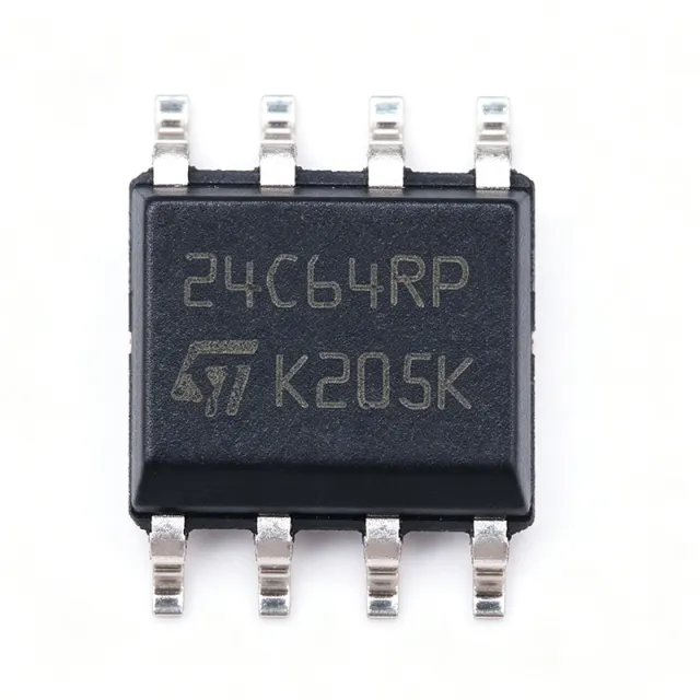
M24C64-RMN6TP - 64Kbit I2C EEPROM | STMicroelectronics
M24C64-RMN6TP

M24C64-RMN6TP - 64Kbit I2C EEPROM | STMicroelectronics

The M24C64-RMN6TP is a 64-Kbit (8K x 8) serial I2C EEPROM from STMicroelectronics, packaged in a compact SO-8 (N) package. It operates over a supply voltage range of 1.8V to 5.5V, with a maximum clock frequency of 1 MHz (for VCC >= 4.5V) and 400 kHz (for VCC >= 2.5V). The device features a byte-write time of 5 ms and a write cycle endurance of 1 million write cycles, with data retention of 40 years. Data verified as of 2026-08-05. An EEPROM (Electrically Erasable Programmable Read-Only Memory) is a non-volatile memory that can be electrically erased and reprogrammed. It is a type of memory IC that retains data when power is removed, making it essential for storing configuration parameters, calibration data, and small amounts of firmware in embedded systems. EEPROMs sit within the memory hierarchy as a non-volatile storage layer, distinct from volatile RAM and higher-capacity flash memory, and are commonly used for byte-level read/write operations in applications requiring frequent updates. Key features include a wide operating voltage range (1.8V to 5.5V), I2C interface with 7-bit device addressing, and a write protect pin for hardware data protection. The device supports sequential read and write operations, and includes a self-timed programming cycle with an internal write cycle time of 5 ms. The SO-8 package is industry-standard, enabling drop-in compatibility with many other 64-Kbit I2C EEPROMs. The M24C64-RMN6TP uses a floating-gate transistor architecture for non-volatile storage, with a charge pump for internal programming voltage generation. The I2C interface supports standard (100 kHz), fast (400 kHz), and fast-plus (1 MHz) modes, allowing flexible integration with microcontrollers. The device includes a write cycle time of 5 ms, which is typical for EEPROMs, and supports a write protect feature to prevent accidental writes. Typical applications include parameter storage in industrial sensors, calibration data in medical devices, configuration storage in networking equipment, and firmware updates in consumer electronics. The wide voltage range and low power consumption make it suitable for battery-powered IoT devices, while the high endurance (1 million cycles) supports frequent data logging. When designing with this device, ensure the I2C bus pull-up resistors are properly sized for the clock frequency and bus capacitance. The write protect pin should be tied to ground if not used, and the device address pins (A0, A1, A2) must be set to avoid conflicts with other I2C devices on the bus. This page synthesizes distributor pricing, drop-in alternatives, and practical design notes not found in the STMicroelectronics datasheet, providing a comprehensive resource for engineers selecting a 64-Kbit I2C EEPROM.

USD $0,08 Contato
M25P16-VMF3PB - 16Mbit SPI NOR Flash 75MHz | Micron
M25P16-VMF3PB

M25P16-VMF3PB - 16Mbit SPI NOR Flash 75MHz | Micron

The Micron Technology M25P16-VMF3PB is a 16 Mbit (2 Mb x 8) serial NOR Flash memory operating on an SPI-compatible bus at clock frequencies up to 75 MHz, supplied at 2.7 V to 3.6 V in a 16-pin SOP2 (16-SO) surface-mount package rated for -40 C to +125 C automotive temperature ranges. Serial NOR Flash is a non-volatile memory category that stores code and data in a NOR array architecture, allowing random access to any address through a simple serial peripheral interface (SPI). In the system memory hierarchy, it sits alongside parallel NOR and NAND Flash as a code-storage device, and is a direct descendant of the Numonyx/ST M25P family later acquired into the Micron portfolio. Compared with parallel Flash, SPI NOR reduces pin count, board area, and controller I/O requirements, which is why it dominates boot-code and firmware-storage roles in embedded designs. Key features of the M25P16-VMF3PB include its 75 MHz maximum clock frequency for fast code shadowing and XIP-style access, 2 Mb x 8 organization with 32 sectors of 64 Kbyte each (4 Kbyte subsector granularity via standard erase commands), advanced write-protection mechanisms, and deep power-down mode for minimum standby consumption. The automotive-grade suffix (PB, extended temperature) supports designs qualified to demanding environmental requirements. Architecturally, the device executes a standard SPI command set: READ and FAST_READ for data retrieval, PAGE PROGRAM for 256-byte page writes, SECTOR ERASE and BULK ERASE for content management, plus status-register and write-protect commands. The dedicated HOLD pin pauses serial communication without releasing the bus, and a hardware reset pin (S_RST on the 16-pin package) allows recovery of the serial interface. Typical applications include boot firmware storage for DSPs and microcontrollers, FPGA configuration bitstreams, parameter and calibration data storage in automotive modules, industrial drives, and set-top-box platforms. When designing with this device, verify hold times at the full 75 MHz clock and decouple VCC with 100 nF close to the supply pin; the 16-SOP2 footprint is wider than the 8-SO variant, so confirm the land pattern before second-sourcing. This page synthesizes distributor pricing, verified drop-in alternatives, and practical design notes not found in the manufacturer datasheet.

Cotação Contato
M25P16-VMF3TPB - 16Mb SPI NOR Flash 75MHz | Micron
M25P16-VMF3TPB

M25P16-VMF3TPB - 16Mb SPI NOR Flash 75MHz | Micron

The Micron M25P16-VMF3TPB is a 16Mb (2Mb x 8) serial NOR Flash memory with an SPI-compatible bus interface, up to 75 MHz clock support, and a 2.7V to 3.6V supply range, housed in a 16-pin SOIC wide-body (SO16W, 300 mil) package with -40C to +125C operation. Serial NOR Flash is a nonvolatile memory that stores code and data and is read over a simple four-wire SPI bus (chip select S, serial clock C, serial data input D, and serial data output Q). In the embedded-systems hierarchy it sits below parallel NOR and DRAM in bandwidth but above I2C EEPROMs in speed and density, making it the de facto standard for boot-code storage in microcontrollers, DSPs, and FPGAs. Key features of the M25P16 include 75 MHz SPI read operation, fast page programming (256-byte pages) and sector erase (64 KB sectors) with block protection, 15 ns clock-to-output access timing, and advanced write-protection mechanisms including status-register and hardware write protect. The VMF3 ordering option denotes the wide 16-pin SO package, RoHS-compliant lead-free construction, and Tape & Reel delivery, with the TP suffix indicating the shipping format. Architecturally, the device is an SLC single-level-cell NOR array organized as 2M x 8 bits, with an internal state machine that executes Read, Fast Read, Page Program, Sector Erase, Bulk Erase, and Write Status Register commands. Micron assigned this part to its Product Longevity Program, which suits multi-year industrial deployments; however, Micron has since EOL'd low-density serial NOR families, so the Renesas-published conversion guide to Adesto FUSION/Standard Flash and the cross-brand equivalents below are relevant for new sourcing. Typical applications include FPGA/DSP boot configuration (for example SHARC DSP boot loaders), BIOS/firmware storage in networking equipment, parameter and calibration data logging in industrial drives, and set-top-box or display firmware storage. Design consideration: hold the HOLD pin high and tie WRITE PROTECT appropriately; use 100 nF decoupling at VCC and respect the deep power-down entry/exit timing to minimize standby current. This page synthesizes verified distributor data, drop-in same-package alternatives, and sourcing guidance for a part affected by Micron EOL - information not consolidated in the manufacturer datasheet.

Cotação Contato
M25P16-VMN3PB - 16Mb SPI NOR Flash 75MHz SOIC-8 | Micron
M25P16-VMN3PB

M25P16-VMN3PB - 16Mb SPI NOR Flash 75MHz SOIC-8 | Micron

The Micron M25P16-VMN3PB is a 16 Mbit (2 M x 8) serial NOR Flash memory with a high-speed SPI-compatible bus, clocking up to 75 MHz, in an 8-pin SOIC (208-mil SO, SOP) package. It is rated for the automotive temperature grade of -40C to +125C and is covered by Micron's Product Longevity Program. Serial NOR Flash is a non-volatile memory category within the broader memory IC and semiconductor hierarchy. Unlike NAND Flash, NOR Flash allows random-access reads of individual bytes, making it the standard choice for firmware boot code storage in embedded systems, where the processor must execute or quickly fetch code directly from the memory array over an SPI bus. Key features of the M25P16 include 16,777,216 bits of SLC (single-level cell) NOR storage organized as 2,097,152 bytes x 8, a 75 MHz maximum SPI clock frequency, 100,000 program/erase cycles endurance, and advanced write-protection mechanisms. Page program and sector erase operations are supported with block-level protection for reliable code and data storage. Architecturally, the device uses a standard SPI interface with signals S (chip select), D (serial data input), Q (serial data output), and C (serial clock), plus WP# (hardware write protect) and HOLD# (pause communication without deselecting). The automotive temperature grade and Product Longevity Program membership make it suitable for long-lifecycle deployments where sourcing continuity matters. Typical applications include automotive modules, industrial controllers, embedded firmware boot storage, data logging, computing modules, and configuration storage for FPGAs and SoCs requiring dependable non-volatile code memory. Design tip: verify VCC decoupling and use hold operations carefully - releasing HOLD# mid-clock requires an edge on C to resume, so keep timing margins in multi-master SPI buses. This page adds distributor pricing tiers, drop-in alternative cross-references, and practical design notes not consolidated in the manufacturer datasheet.

Cotação Contato
M25P16-VMN3YPB - 16Mbit SPI NOR Flash 75MHz SOIC-8 | Micron
M25P16-VMN3YPB

M25P16-VMN3YPB - 16Mbit SPI NOR Flash 75MHz SOIC-8 | Micron

The Micron M25P16-VMN3YPB is a 16Mbit (2MB) serial NOR Flash memory with an SPI interface operating up to 75 MHz, supplied in an 8-pin SOIC (8-SO, 3.90 mm width) package with automotive temperature grade. It stores data as 16M x 1 bits and uses a standard SPI command set for read, page program, and sector erase operations. Serial NOR Flash is a nonvolatile memory category within the memory IC hierarchy (Flash memory -> NOR Flash -> serial/SPI NOR Flash -> nonvolatile semiconductor memory). Unlike parallel NOR devices, SPI NOR Flash uses a reduced pin count (8 pins) communicating over a clocked serial bus, which makes it ideal for storing boot code, firmware, and configuration data in space-constrained embedded systems. Key features of the M25P16-VMN3YPB include its 16Mbit density organized for x1 SPI access, a 75 MHz maximum clock frequency for fast code-shadowing reads, and an automotive temperature grade per distributor data (Partstack/Vyrian list Temperature Grade: AUTOMOTIVE), supporting -40C to +125C environments. The 8-SOIC footprint is industry-standard, easing second-source qualification. Architecturally, the device is organized into pages for programming and larger sectors for erase, with the standard Micron M25P family command set (READ, FAST_READ, PAGE PROGRAM, SECTOR ERASE, BULK ERASE, write protection via the /W pin, and /HOLD for bus suspension). This command compatibility is why the M25P16 is frequently cross-referenced by vendors such as STMicroelectronics and Winbond equivalents in the same SOIC-8 footprint. Typical applications include FPGA configuration bitstream storage, microcontroller boot firmware, automotive infotainment and body-control module code storage, LCD display panel parameter memory, and communication equipment configuration storage. The 75 MHz SPI clock supports fast boot-time readout where a quad interface is not required. Design consideration: verify the supply range and pin functions against the manufacturer datasheet before drop-in substitution; the /W (write-protect) and /HOLD pins must be driven correctly by the host, as not all competitor devices define identical hold behavior. This page synthesizes distributor pricing, stock data, drop-in alternatives, and practical design notes not found in a single datasheet, giving engineers a complete qualification-ready view of the M25P16-VMN3YPB.

Cotação Contato
M25P16-VMN6P - 16Mb SPI NOR Flash 75MHz SOIC-8 | Micron
M25P16-VMN6P

M25P16-VMN6P - 16Mb SPI NOR Flash 75MHz SOIC-8 | Micron

The Micron M25P16-VMN6P is a 16-Mbit (2 Mbit x 8) serial NOR Flash memory device with an SPI-compatible bus interface, packaged in an 8-pin SOIC (SO8) with 75 MHz maximum clock frequency. It features advanced write-protection mechanisms including block-lock protect bits and a hardware write-protect pin, and operates from a single 2.7 V to 3.6 V supply. The device delivers typical page-program time of 1.4 ms for up to 256 bytes, sector-erase time of 0.65 s, and bulk-erase time of 4 s, with JEDEC-standard SFDP (Serial Flash Discoverable Parameters) read access. A NOR Flash memory is a non-volatile storage technology that retains data without power and supports random (byte-level) read access, unlike NAND Flash which is read sequentially by page. The NOR architecture makes it ideal for code storage and execute-in-place (XIP) boot ROM applications where deterministic, low-latency reads are required at system power-up. The SPI (Serial Peripheral Interface) bus reduces pin count versus parallel NOR, allowing the device to share a 4-wire (or 3-wire) bus with other peripherals and saving PCB area in compact embedded designs. Key specifications include a 75 MHz SPI clock (50 MHz for legacy read commands), 32-Kbyte and 64-Kbyte sector architecture, JEDEC 2-byte electronic signature, and an industry-standard command set compatible with many prior-generation SPI Flash devices. The 8-pin SOIC package provides 3 mm x 4.9 mm board area, supporting both commercial (0 C to 70 C) and industrial (-40 C to +85 C) operating ranges. The M25P16 architecture uses a single 2.7-3.6 V supply, on-chip write/erase voltage generation, and a deep power-down mode drawing typically 1 uA for battery-backed applications. Hardware sector protection and software block-lock bits allow designers to enforce bootloader read-only zones for secure firmware-update implementations. Typical applications include router firmware storage, IoT sensor node boot memory, set-top box data logging, industrial PLC parameter storage, and consumer electronics such as printers and smart-home gateways where small-footprint code and parameter storage is required. Compared to EEPROM, NOR Flash provides higher density per die at lower cost per Mbit but requires block-level erase before write. When designing with this device, ensure VCC decoupling of 100 nF plus 4.7 uF is placed within 5 mm of the VCC pin to suppress write/erase inrush transients. The /WP and /HOLD pins must be tied to VCC (or pulled high) if unused, and the /CS line must be returned to logic high between commands to reset the SPI state machine.

Cotação Contato
M25P20-VMN3PB - 2Mbit SPI NOR Flash 75MHz SOIC-8 | Micron
M25P20-VMN3PB

M25P20-VMN3PB - 2Mbit SPI NOR Flash 75MHz SOIC-8 | Micron

The Micron M25P20-VMN3PB is a 2 Mbit (256 Kbyte) low-voltage serial NOR Flash memory with a 75 MHz SPI bus interface, housed in an 8-pin SOIC (SOP-8) package. It operates from a 2.7V to 3.6V single supply over a -40C to +125C temperature range. Serial NOR Flash is a nonvolatile memory category in which data is read, programmed, and erased over a serial peripheral interface (SPI) rather than a parallel bus. Within the memory hierarchy it sits under Flash memory -> NOR Flash -> serial/quad SPI memory, and is widely used for code storage (XIP), FPGA configuration, and parameter logging because it offers random-access-like byte readability, high reliability, and a minimal pin count. Key features of the M25P20 include a 2 Mbit organization (256 Kbytes, 4 sectors of 512 Kbit each, 256-byte pages), page program times of 0.8 ms typical for up to 256 bytes, sector erase of 0.6 s typical (512 Kbit), and bulk erase of 3 s typical. The 75 MHz SPI clock rate supports fast code fetch and configuration downloads. Write protect and hold functions are provided on dedicated pins for hardware data protection and bus sharing. The M25P20 uses Micron NOR Flash cell technology with a standard SPI command set (READ, FAST_READ, PAGE PROGRAM, SECTOR ERASE, BULK ERASE, WRITE ENABLE/DISABLE, READ STATUS), making it command-compatible with many industry-standard serial Flash devices and simplifying firmware reuse. The VMN3 package option is lead-free (Pb-free) and RoHS compliant, and the device supports an extended industrial temperature range. Typical applications include FPGA configuration bitstream storage, embedded microcontroller code and data storage, LCD panel and display controller firmware, networking equipment boot code, and industrial automation parameter storage. The small SOIC-8 footprint suits space-constrained boards. For design, keep SPI trace lengths short and use series termination near the source when operating at the full 75 MHz clock rate; decouple VCC with a 100 nF ceramic capacitor close to pin 8. This page synthesizes distributor pricing, verified drop-in alternatives, pinout data, and practical design notes not consolidated in the manufacturer datasheet.

Cotação Contato
M25P20-VMN3TPB - 2Mb SPI NOR Flash 75MHz SOIC-8 | Micron
M25P20-VMN3TPB

M25P20-VMN3TPB - 2Mb SPI NOR Flash 75MHz SOIC-8 | Micron

The Micron M25P20-VMN3TPB is a 2 Mbit (256K x 8) low-voltage serial NOR Flash memory with a 75 MHz SPI-compatible bus interface, housed in an 8-pin SOIC (SO, 0.150 inch, 208 mil) package supplied in tape and reel. Operating from 2.3 V to 3.6 V (2.5 V/3.3 V supply class), it delivers page programming of up to 256 bytes in 0.8 ms typical and an 8 ns access time. Serial NOR Flash is a nonvolatile memory category that stores code and data electrically and reads them out over a serial peripheral interface (SPI). In the system memory hierarchy it sits below DRAM and parallel NOR: it holds firmware, boot code, configuration bitstreams, and calibration tables that must survive power loss, trading parallel bandwidth for a minimal pin count and tiny footprint. SPI NOR is the de facto standard for boot memory in microcontroller, FPGA, and SoC platforms. Key features of the M25P20 include 75 MHz clock support for high-performance read commands, 2 Mbit density organized as 4 sectors of 512 Kbit each, sector erase in 0.6 s typical and bulk erase in 3 s typical, and advanced write-protection mechanisms. The -40C to +125C operating range supports industrial and automotive-adjacent environments, and product longevity commitments apply. Architecturally, the device uses a single-level NOR cell array addressed via SPI commands, with write-enable latching, status register polling, and hardware/software protection schemes preventing accidental program or erase. The VMN3 speed grade runs the full 75 MHz command set over the industrial temperature range. Typical applications include FPGA configuration storage, boot code memory for embedded processors, parameter and calibration storage in industrial drives, and firmware storage in networking and consumer equipment. Design consideration: keep the SPI clock and data traces short, place a 0.1 uF decoupling capacitor directly at the VCC pin, and respect the hold and write-protect pin states during power ramp-up to prevent spurious writes. This page synthesizes distributor pricing, same-family drop-in alternatives, pinout, and practical design notes not consolidated in the manufacturer datasheet.

Cotação Contato
M25P32-VMW3GB - 32Mbit SPI NOR Flash 75MHz | Micron
M25P32-VMW3GB

M25P32-VMW3GB - 32Mbit SPI NOR Flash 75MHz | Micron

The Micron M25P32-VMW3GB is a 32Mbit (4M x 8) serial NOR flash memory with a 75 MHz SPI bus interface, 3.0 V to 3.6 V supply voltage, and an 8-pin SOIC wide-body (VMW, 208-mil SOIC-8 W) package. It is AEC-Q100 qualified for automotive applications and supports page program, sector erase, and bulk erase operations with hardware and software write protection. Serial NOR flash is a nonvolatile memory category in which data is accessed byte-wise over a serial peripheral interface (SPI) rather than a wide parallel bus. Within the memory hierarchy - memory IC -> flash memory -> NOR flash -> serial SPI NOR flash - these devices trade raw bandwidth for dramatically reduced pin count, tiny board footprint, and low cost, which is why they are the de facto standard for storing boot code, firmware images, and configuration data in embedded systems. Key features of the M25P32-VMW3GB include the 75 MHz maximum SPI clock frequency for fast firmware downloads, a 256-byte page with typical 0.8 ms page programming time, uniform 64-Kbyte sectors with 64 sectors total, and a deep power-down mode that reduces standby current to approximately 1 microamp. The device supports SPI modes 0 and 3, operates from a single 3.3 V supply, and offers hardware write protection on the /WP pin plus block-level software protection. Architecturally, the M25P32 inherits the Numonyx/ST M25P family design later acquired by Micron, using floating-gate NOR cells with a state machine handling the standard SPI command set (READ, FAST_READ, PAGE PROGRAM, SECTOR ERASE, BULK ERASE, WRITE ENABLE/DISABLE, READ STATUS).JEDEC-standard 16-bit signatures allow electronic signature identification for programmer compatibility. Typical applications include BIOS/firmware storage in automotive ECUs, boot code for FPGAs and microcontrollers, configuration storage in industrial drives and set-top boxes, and parameter logging in network equipment. Its AEC-Q100 qualification makes it a preferred choice for automotive temperature environments. Design tip: use FAST_READ at 75 MHz only after verifying your PCB signal integrity; at high clock rates, keep traces short and add series termination on SCK. This page synthesizes distributor pricing, drop-in alternatives, and practical design notes not found in the manufacturer datasheet.

Cotação Contato
M25P40-VMB3TPB - 4Mb SPI NOR Flash 75MHz | Micron Technology
M25P40-VMB3TPB

M25P40-VMB3TPB - 4Mb SPI NOR Flash 75MHz | Micron Technology

The Micron M25P40-VMB3TPB is a 4Mb (512Kb x 8) serial NOR flash memory with a high-speed SPI-compatible bus interface supporting clock frequencies up to 75MHz, a supply voltage range of 2.3V to 3.6V, and an operating temperature range of -40C to +125C, housed in an 8-pin UFDFPN (2x3 mm) ultra-thin fine-pitch package. A serial NOR flash memory is a nonvolatile storage device that retains code and data without power and is read byte-by-byte over a serial bus, most commonly SPI (Serial Peripheral Interface). In the system memory hierarchy, NOR flash sits alongside parallel NOR, NAND flash, and EEPROM as a class of nonvolatile memory ICs, and it is the dominant choice for storing boot code in embedded systems because it offers random-access read behavior and high reliability. Key features of the M25P40 include 4Mb density organized as 512Kb x 8, 75MHz SPI clock operation for fast code fetch, advanced write-protection mechanisms, a wide 2.3V to 3.6V single supply, and an extended -40C to +125C industrial temperature range. The 8-UFDFPN (2x3 mm) package saves board space versus SOIC-8, making it suitable for compact designs. Architecturally, the device is accessed by a standard SPI bus using chip-select (S#), serial clock (C), serial data input (D), and serial data output (Q) signals, with HOLD# for bus suspension and WP# for hardware write protection. Sector and bulk erase operations, page programming, and status-register-based software protection are managed through standard commands, and the write-protection scheme protects the entire memory or individual sectors against accidental programming. Typical applications include firmware and boot-code storage in industrial controllers, consumer electronics, networking equipment, set-top boxes, printers, and automotive-adjacent body electronics where a small, reliable, low-voltage code flash is required. The 125C rating supports harsh industrial environments. When designing with this device, verify that your SPI controller supports the required 75MHz timing with adequate setup/hold margins, and budget erase/program times in your firmware update routines. Add proper decoupling on VCC and keep the clock line short to maintain signal integrity. This page synthesizes distributor pricing, drop-in alternatives, pinout data, and practical design notes not found in the manufacturer datasheet.

Cotação Contato
M25P40-VMN3PB - 4Mbit SPI NOR Flash 75MHz | Micron
M25P40-VMN3PB

M25P40-VMN3PB - 4Mbit SPI NOR Flash 75MHz | Micron

The Micron M25P40-VMN3PB is a 4 Mbit (512K x 8) serial NOR Flash memory with a high-speed SPI-compatible bus interface up to 75 MHz, a 2.3 V to 3.6 V single supply range, and an operating temperature of -40C to +125C, housed in an 8-pin SOIC (3.90 mm width) package supplied in tubes. This industrial/automotive-temperature-grade member of the M25P40 family is covered by Micron's Product Longevity Program (program start date 5/4/2011). Serial NOR Flash is a nonvolatile memory category that stores code and data without power and is read through a serial peripheral interface (SPI) rather than a wide parallel bus. In the memory hierarchy it sits among low-density code-storage devices used for firmware boot, parameter storage, and FPGA/configuration loading, complementing DRAM (working memory) and high-density NAND Flash (mass storage). Key features include 4 Mbit of Flash organized x8, SPI bus compatibility (modes 0 and 3), 75 MHz clock operation for high-performance read commands, advanced write-protection mechanisms, and a low-voltage 2.3 V-3.6 V single supply. The -40C to +125C range and Product Longevity Program membership make it suitable for long-lifecycle embedded designs. Architecturally, the M25P40 divides the 4 Mbit array into uniform 64 Kbyte sectors that are independently erasable, with 256-byte page programming via the PAGE PROGRAM command. Standard SPI commands cover READ, FAST_READ, SECTOR ERASE, BULK ERASE, WRITE ENABLE, and status-register access; hardware write protect (WP#) and HOLD# pins support in-system control and bus sharing. Typical applications include boot-code and firmware storage in industrial controllers, configuration image storage for FPGAs and CPLDs, set-top boxes, networking line cards, and automotive modules operating across the full -40C to +125C range. Design consideration: note that Micron has announced end-of-life for low-density serial NOR products, so new designs should evaluate the alternatives listed on this page and qualify a second source early. This page synthesizes distributor pricing, drop-in alternatives, and EOL replacement guidance not found in the manufacturer datasheet.

Cotação Contato
M25P40-VMN3TPB - 4Mb SPI NOR Flash 75MHz | Micron
M25P40-VMN3TPB

M25P40-VMN3TPB - 4Mb SPI NOR Flash 75MHz | Micron

The Micron M25P40-VMN3TPB is a 4 Mbit (512K x 8) serial NOR Flash memory with a high-speed SPI-compatible bus interface supporting clock frequencies up to 75 MHz, operating from a single 2.3 V to 3.6 V supply in an 8-pin SOIC (SO, 3.90 mm width) package rated from -40C to +125C for automotive-grade environments. A serial NOR Flash memory is a nonvolatile semiconductor that stores code and data and reads it byte-by-byte over a serial bus. Within the memory hierarchy it sits in the code-storage class of the Flash memory family, below parallel NOR in pin count and above EEPROM in density, making it a standard boot-memory choice for embedded processors. Key features include 4 Mbit of Flash organized as 512K x 8 bits, a 75 MHz SPI bus interface for fast code execution (XIP), a 2.3 V to 3.6 V single supply for 3.3 V and low-voltage systems, advanced write-protection mechanisms, and sector/block erase architecture with page programming. Automotive temperature range -40C to +125C supports under-hood and industrial deployments. The device uses a standard SPI command set with read, fast-read, page program, sector erase, bulk erase, and write-protect commands. The HOLD# pin suspends serial communication without deselecting the device, and the W# pin provides hardware write protection, while status-register software protection guards against accidental program or erase operations. Typical applications include BIOS/code storage in automotive ECUs, boot memory for microcontrollers and FPGAs, configuration storage in industrial automation, and parameter storage in networking and consumer equipment where a small-footprint 8-SOIC nonvolatile memory is required. Design consideration: at 75 MHz keep SPI trace lengths short and match clock-to-data skew; use 10 k ohm pull-ups on HOLD# and W# to prevent accidental state changes during power-up. This page synthesizes distributor pricing, drop-in alternatives within the Micron M25P family, pinout data, and practical design notes not found in the manufacturer datasheet alone.

Cotação Contato
M25P40-VMP6TGB - 4Mb SPI NOR Flash 75MHz VFQFPN-8 | Micron
M25P40-VMP6TGB

M25P40-VMP6TGB - 4Mb SPI NOR Flash 75MHz VFQFPN-8 | Micron

The Micron M25P40-VMP6TGB is a 4 Mbit (512 K x 8) serial NOR Flash memory with SPI bus interface, operating from a single 2.3 V to 3.6 V supply and delivering a 75 MHz maximum clock rate in an 8-pin VFQFPN-EP (MLP8, 6x5 mm) tape-and-reel package. A serial NOR Flash is a non-volatile memory that stores data persistently and communicates with a host controller over a low-pin-count synchronous protocol such as SPI. Within the memory hierarchy, NOR Flash sits between EPROM/EEPROM and NAND Flash: it offers random byte-level read access like EEPROM but at much higher density, and unlike NAND it supports execute-in-place (XiP) directly from the array. This part belongs to the SPI NOR Flash family, the dominant standard for boot, configuration, and firmware storage in microcontrollers, FPGAs, and consumer devices. Key features include Page Program of up to 256 bytes in 0.8 ms (typical), Sector Erase of 512 Kbit in 0.6 s (typical), and Bulk Erase of the full 4 Mbit in 4.5 s (typical). Deep Power-down mode draws only 1 uA (typical), and Hardware Write Protection is configurable through three non-volatile bits (BP0, BP1, BP2) to lock out a defined protected area. The single 2.3-3.6 V supply simplifies integration with 3.3 V MCUs and 3 V FPGAs. The device is organized as 512 K x 8 with an 8 ns access time, implemented as a NOR architecture with hardware-accelerated page programming and sector-erase blocks. The 75 MHz SPI clock supports fast code-shadowing and XiP boot, while the deep power-down mode enables battery-friendly idle states. The VFQFPN-EP package provides a low thermal-resistance path and a compact footprint for space-constrained designs. Typical applications include boot and firmware storage for microcontrollers and FPGAs, IoT and smart-home sensor hubs, industrial control and metering, automotive infotainment and cluster code storage, and consumer electronics such as set-top boxes and printers. The 4 Mbit density is well suited to small boot images, lookup tables, and parameter sets. When designing with this device, ensure the host SPI controller supports the JEDEC-standard SFDP-less instruction set (READ, PAGE PROGRAM, SECTOR ERASE, BULK ERASE, READ-ID, READ-STATUS) and that CS# is returned high between commands. Decouple VCC with a 100 nF ceramic capacitor close to the pin and observe the datasheet timing for tSE and tBE during in-application updates. This page synthesizes distributor pricing, drop-in alternates from the same M25P40 family and cross-brand SPI NOR alternatives, pinout, and practical design notes that go beyond a generic datasheet summary.

Cotação Contato
M25P64-VMF3PB - 64Mbit SPI NOR Flash 75MHz | Micron
M25P64-VMF3PB

M25P64-VMF3PB - 64Mbit SPI NOR Flash 75MHz | Micron

The Micron Technology M25P64-VMF3PB is a 64 Mbit (8M x 8) serial NOR Flash memory with a 75 MHz SPI bus interface, operating from a 2.7 V to 3.6 V single supply voltage, housed in a 16-lead SOIC wide-body (16-SOP) surface-mount package. The -3P suffix denotes the automotive temperature grade, making this device suited to harsh-environment embedded designs. A serial NOR Flash memory is a non-volatile semiconductor memory that stores code and data and is accessed byte-by-byte over a serial peripheral interface (SPI). Within the memory hierarchy it sits alongside parallel NOR and serial NAND devices; because it offers random-access read capability, it is the dominant boot-memory choice for microcontrollers, FPGAs, and SoCs in the power management IC and semiconductor ecosystem. Key features of the M25P64 include 64 Mbit of Flash memory density, SPI-bus-compatible serial interface with clock rates up to 75 MHz, a 3 V class single supply (2.7 V to 3.6 V), sector and bulk erase operations, and a hardware write-protect pin. Automotive qualification and RoHS-compliant, lead-free packaging distinguish this variant for industrial and vehicular deployments. The device is organized as 8M words of 8 bits, with page-program and sector-erase commands defined in the M25P command set inherited from the Numonyx (STMicroelectronics) product line now owned by Micron. Page programming and fast read operations allow embedded bootloaders and configuration loaders to fetch FPGA bitstreams or MCU firmware efficiently over just four signal lines (S, C, D, Q), reducing pin count and PCB routing complexity versus parallel Flash. Typical applications include FPGA configuration storage (notably for Microsemi/Microchip RTAX and ProASIC3 radiation-tolerant and space-adjacent platforms), automotive ECU boot memory, and industrial firmware storage where non-volatile code retention and SPI simplicity are essential. For design, hold and write-protect timing must be respected during power sequencing, and the 75 MHz clock requires careful SPI signal-integrity layout with series termination on the clock line. This page synthesizes distributor pricing, drop-in alternatives, and practical design notes not found in the manufacturer datasheet.

Cotação Contato
M25P64-VMF3TPB - 64Mbit SPI NOR Flash 75MHz | Micron
M25P64-VMF3TPB

M25P64-VMF3TPB - 64Mbit SPI NOR Flash 75MHz | Micron

The Micron Technology M25P64-VMF3TPB is a 64 Mbit (8M x 8) serial NOR Flash memory with an SPI-compatible bus interface, a 75 MHz maximum clock frequency, and a 3.0 V (2.7 V to 3.6 V) single supply, housed in a 16-pin wide-body SOIC (16-SOIC W, 7.50 mm / 300 mil body, tape and reel packaging). A serial NOR Flash memory is a non-volatile memory device that stores code and data while retaining contents without power, and is accessed byte-by-byte over a serial interface. In the memory hierarchy, NOR Flash sits alongside NAND Flash and EEPROM within the non-volatile memory family; unlike NAND, NOR supports direct random access to any address, which makes it the standard choice for direct code execution (XIP) of bootloaders and firmware in embedded systems. Key features include the 64 Mbit density organized as 8,388,608 bytes, SPI Mode 0 and Mode 3 operation at up to 75 MHz, hardware and software write-protection mechanisms (block protect and status register protection), sector erase and bulk erase instructions, and an automotive temperature grade suitable for -40C to +85C (and beyond, per grade coding) environments. The HOLD pin suspends serial communication without deselecting the device, useful in multi-slave SPI buses shared with real-time tasks. Architecturally, the M25P64 family uses a page-program architecture: data is programmed page-by-page into a buffer and then written to the array, with erase granularity at sector level. The 75 MHz SPI clock, combined with fast read and fast read dual-output style throughput, keeps boot times short for large firmware images, while the 8 ns access-time class reflects the internal read latency of the array. Typical applications include automotive ECU code and calibration storage, FPGA configuration boot memories in industrial and communications equipment, and firmware storage in set-top boxes, networking line cards, and telemetry modules where reliability and long-term availability matter. Design consideration: keep the SPI trace lengths short and add a 100 nF decoupling capacitor directly across VCC and GND; ensure the HOLD and WRITE PROTECT pins are actively driven to avoid floating-pin command corruption during power ramps. This page synthesizes distributor pricing and stock references, verified cross-references, and practical drop-in alternative analysis not consolidated in the manufacturer datasheet.

Cotação Contato
M25P80-VMN3TPB - 8Mbit SPI NOR Flash 75MHz SOIC-8 | Micron
M25P80-VMN3TPB

M25P80-VMN3TPB - 8Mbit SPI NOR Flash 75MHz SOIC-8 | Micron

The Micron M25P80-VMN3TPB is an 8Mbit (1M x 8) serial NOR Flash memory device with advanced write-protection mechanisms, accessed through a high-speed SPI-compatible bus, housed in an 8-pin SOIC (3.90mm width) package. It operates from a single 2.7V to 3.6V supply and supports clock frequencies up to 75 MHz. Serial NOR Flash is a non-volatile memory category within the broader Flash memory hierarchy (memory IC -> Flash memory -> NOR Flash -> serial SPI NOR Flash). Unlike parallel Flash, serial NOR uses a reduced pin count SPI interface, trading some bandwidth for board space, simplicity, and lower cost, which makes it the dominant choice for code storage in embedded systems. Key features include the 75 MHz maximum clock rate, page programming of up to 256 bytes in 0.64 ms typical, sector erase capability, and hardware and software write protection. The JEDEC-standard SPI command set and dedicated write-protect and hold pins simplify integration with virtually any microcontroller with an SPI peripheral. Architecturally, the device is organized as 16 sectors of 64 KB (1 Mbyte total), with page program and bulk/sector erase commands managed by an internal state machine. Supply range of 2.7V to 3.6V makes it compatible with standard 3.3V logic rails, and the hold pin allows the serial bus to be paused without deselecting the device. Typical applications include boot code and firmware storage for microcontrollers and FPGAs, parameter and calibration data storage in industrial equipment, and configuration memory in networking and consumer electronics. The SPI interface and small SOIC-8 footprint fit space-constrained embedded designs. Design consideration: honor the sector erase before page program requirement - the M25P80 can only program bits from 1 to 0, so software must erase (setting bits back to 1) at 64 KB sector granularity before rewriting, which influences firmware update layout. This page synthesizes distributor pricing, drop-in alternatives, cross-reference data, and practical design notes not found in the manufacturer datasheet.

Cotação Contato
M25PE16-VMW6TG - 16Mbit SPI NOR Flash 75MHz SOIC-8 | Micron
M25PE16-VMW6TG

M25PE16-VMW6TG - 16Mbit SPI NOR Flash 75MHz SOIC-8 | Micron

The Micron M25PE16-VMW6TG is a 16-Mbit (2 Mb x 8) Serial Paged NOR Flash memory with byte-alterability, accessed via an SPI-compatible bus running at up to 75 MHz, packaged in an 8-pin SOIC (0.209 inch / 5.30 mm width) wide-body. The M25PE16-VMW6TG operates from a single low-voltage supply and supports page erase, page program, and bulk erase operations. It provides 16,777,216 bits of storage organised as 2,097,152 bytes. A Serial NOR Flash is a non-volatile memory device that combines the density of traditional parallel flash with the pin-efficiency of a serial peripheral interface. NOR Flash (named after the NOR gate logic mapping of its cell array) supports random read access and execute-in-place (XIP) operation, allowing microcontrollers to fetch code directly from flash without first copying it into RAM. Within the memory hierarchy, NOR Flash sits above EEPROM and below SRAM/DRAM in the storage hierarchy: slower than RAM but non-volatile, and faster than NAND Flash with byte-level read granularity. Key specifications include 75 MHz maximum SPI clock, 50 MHz or 75 MHz variant (per datasheet publication), 256-byte page size for programming, 4 to 64 Kbyte sector/sub-sector erase granularity, JEDEC-standard 3-byte identification (SFDP optional on some revisions), and a wide operating voltage range suitable for 2.5 V and 3.3 V system rails. The device supports standard SPI mode 0 and mode 3, with optional dual/quad I/O on related part numbers. The architecture combines a uniform 64-Kbyte main block erase granularity with finer 4-Kbyte sub-sector erase capability, enabling flexible firmware storage and bootloader protection schemes. Byte-alterability allows individual bytes to be reprogrammed without first erasing an entire sector (a feature distinguishing the M25PE family from traditional NOR Flash that requires block erase before rewrite). Typical applications include firmware storage for IoT devices, data logging in industrial sensors, configuration parameter storage in networking equipment, code shadowing for microcontroller boot ROMs, and automotive infotainment boot memory. The page-erasable architecture makes it well suited for applications requiring frequent small-block updates. When designing with this part, observe the JEDEC-standard SPI timing requirements and provide adequate VCC decoupling close to the IC. The Write Enable (WREN) command must precede any program/erase operation; failure to issue WREN causes the command to be ignored silently. This page synthesises distributor pricing, drop-in alternatives (including ST-Microelectronics-sourced equivalents and Adesto/Renesas cross-reference candidates) and practical design notes not found in the standalone manufacturer datasheet.

Cotação Contato
M25PX80-VMN3TPB - 8Mb SPI NOR Flash 75MHz | Micron
M25PX80-VMN3TPB

M25PX80-VMN3TPB - 8Mb SPI NOR Flash 75MHz | Micron

The Micron Technology M25PX80-VMN3TPB is an 8 Mbit (1 M x 8) serial NOR Flash memory device with an SPI-compatible bus operating at up to 75 MHz, a 2.7 V to 3.6 V supply range, and an 8-pin SOIC (3.90 mm width) surface-mount package. Serial NOR Flash is a nonvolatile memory category that stores code and data without power, accessed over a reduced-pin-count SPI bus (chip select, serial clock, data-in, data-out). In the memory hierarchy it sits alongside parallel NOR and NAND Flash: NOR offers fast random read access ideal for execute-in-place (XIP) code storage, while the SPI interface reduces pin count, board area, and cost compared with parallel devices. Key features of the M25PX80 include the 75 MHz maximum SPI clock, dual input/output read commands that double transfer bandwidth for read and program operations, and advanced write-protection mechanisms documented in the M25PX80 datasheet. The device supports block and sector erase architectures typical of the M25PX family, with a 3V/3.3V operating voltage class suited to embedded processors, microcontrollers, and FPGA configuration loads. Architecturally, the M25PX80 uses a single-die NOR array with an SPI command set compatible with the widely deployed M25P family, adding enhanced programming performance and enhanced protection features. The VMN3 suffix denotes the 8-SOIC 150-mil package in tape-and-reel packing; the PB suffix indicates automotive temperature and quality flow, and the device is listed as AEC-Q100 qualified on Arrow.com. Typical applications include FPGA boot/configuration storage, MCU code and parameter storage in industrial controls, set-top boxes, networking line cards, and automotive body/comfort modules where a compact 8-pin footprint and Q-qualified flow are required. Design consideration: because the part is reported obsolete, new designs should plan a second source or footprint-compatible successor; verify hold and write-protect pin usage, as external pull-ups on HOLD# and W# are required when these functions are not actively driven. This page synthesizes distributor pricing, drop-in alternatives, lifecycle status, and practical design notes not found in the manufacturer datasheet.

Cotação Contato
M27C512-12F - 512Kbit (64Kx8) 120ns UV EPROM CDIP-28 | STMicroelectronics
M27C512-12F

M27C512-12F - 512Kbit (64Kx8) 120ns UV EPROM CDIP-28 | STMicroelectronics

The STMicroelectronics M27C512-12F is a 512 Kbit (64K x 8) ultraviolet-erasable programmable read-only memory (UV EPROM) with a 120 ns access time, housed in a 28-pin ceramic DIP (CDIP-28) Frit Seal with window package. It operates from a single 5 V supply, draws 30 mA active and 100 µA standby, and is organized as 65,536 bytes for byte-wide read access through standard address and data buses. The M27C512-12F belongs to the M27C512 family of UV EPROM and OTP EPROM devices, designed for fast turn-around and pattern experimentation in microprocessor development, firmware storage, and legacy industrial systems. A UV EPROM (ultraviolet-erasable programmable read-only memory) is a type of non-volatile memory that retains its contents when power is removed and is erased by exposing the die to ultraviolet light through a quartz window in the package. The memory cell is a single FAMOS (floating-gate avalanche-injection MOS) transistor per bit, programmed by hot-electron injection and erased by photo-emission of stored charge. EPROM sits within the non-volatile memory hierarchy between mask ROM and EEPROM/Flash, and is most often used today for development, retro-computing, and industrial legacy systems where byte-wide parallel access and proven long-term retention are valued over in-system reprogrammability. Key features of the M27C512-12F include 120 ns access time (suitable for 8 MHz microprocessors without wait states), low active current of 30 mA and standby current of 100 µA for power-sensitive designs, JEDEC-standard pinout compatibility with the 27C512 family, and 28-pin Frit Seal ceramic DIP packaging with UV-transparent window for erasure. The device supports TTL-compatible inputs and three-state outputs, and is programmed with a 12.5 V VPP supply via a standard EPROM programmer. The M27C512 architecture uses a single-transistor FAMOS cell with on-chip latches for addresses and a 64 K x 8 organization, achieving byte-wide read access and full static operation (no clock required). The CMOS process provides low power consumption and high noise immunity, while the silicon-gate design ensures long-term data retention measured in decades. Program verification is performed with VPP at 12.5 V and VCC at 5 V. Typical applications include 8051-family microcontroller firmware storage, industrial PLC and CNC bootloader ROM, retrocomputing and arcade game cartridge ROM, automotive engine-control firmware (legacy systems), and instrumentation firmware. The M27C512 is also widely used in development environments where rapid erase/reprogram cycles are needed before committing to OTP or masked ROM parts. When designing with the M27C512-12F, ensure proper VPP programming voltage handling and observe maximum ratings to avoid permanent damage. Use a proper EPROM eraser (UV lamp at 253.7 nm) for erasure, and decouple VCC close to the device with a 0.1 µF ceramic capacitor. Note that the ceramic windowed package is ESD-sensitive and should be handled with standard CMOS precautions. This page synthesizes distributor stock data, drop-in same-package alternatives, and practical design notes not found in the manufacturer datasheet alone, helping engineers source and integrate this legacy UV EPROM part.

Cotação Contato