CIs de Interface
Subcategorias
Produtos (1151)

LAN7801T-I/9JX - USB 3.1 Gen1 to GbE Bridge | Microchip | RGMII
The Microchip LAN7801T-I/9JX is a SuperSpeed USB 3.1 Gen 1 to 10/100/1000 Gigabit Ethernet bridge controller delivering high-performance USB-to-RGMII connectivity in a 64-pin SQFN (9x9 mm) package with industrial temperature rating. It integrates a USB 3.1 Gen 1 PHY, a 10/100/1000 Ethernet MAC with RGMII interface to an external PHY, and a 1.8V/3.3V mixed-voltage I/O ring for direct connection to common Ethernet PHYs. A USB-to-Ethernet bridge controller is a category of interface IC that allows a host processor or embedded system lacking native Gigabit Ethernet access to add wired network connectivity through a USB port, typically used where the host has no MII/RGMII-capable MAC or where USB is the only exposed peripheral interface. The product sits in the hierarchy of USB bridge controllers -> network interface controllers -> interface ICs -> integrated circuits, and is commonly deployed as a drop-in network upgrade in designs that need 1 Gbps without redesigning the host platform. Key features of the LAN7801T-I/9JX include USB 3.1 Gen 1 (5 Gbps) SuperSpeed support with backward compatibility to USB 2.0 High-Speed/Full-Speed/Low-Speed, integrated 10/100/1000 MAC, RGMII v1.3 / v2.0 (reduced and core modes) interface to external PHY, jumbo frame support up to 9 KB, Energy-Efficient Ethernet (EEE) per IEEE 802.3az, and industrial -40C to +85C operating range. The part supports CDC-NCM, CDC-ECM, and proprietary Windows/Linux/macOS drivers for plug-and-play integration across operating systems. The device uses a single 25 MHz reference clock (with optional 125 MHz syncE), integrates PHY-side terminations, and provides hardware-offload for checksum, TCP Segmentation Offload, and IEEE 1588 timestamping (depending on driver/firmware revision). Power management includes multiple suspend states (U1/U2 USB, energy detect, magic packet wake), making it suitable for always-on but low-power edge platforms. Typical applications include USB-to-Ethernet dongles and docking stations, industrial PCs and gateways, network printers, NAS enclosures, embedded Linux boards needing GbE, point-of-sale (POS) terminals, automotive infotainment, and ruggedized tablets. The LAN7801T-I/9JX is the industrial-temp (I) variant supplied in Tape & Reel packaging. When designing with this part, pay attention to PCB layout: route the 90-ohm differential USB 3.1 SuperSpeed pairs and RGMII traces with strict length-matching, keep the 25 MHz crystal within 200 mils of XI/XO, and provide a solid ground reference plane beneath the exposed pad for thermal and return-path integrity. This page synthesizes distributor pricing, drop-in alternatives from the Microchip LAN78xx family and cross-brand USB-to-Ethernet bridges, and practical design notes not found in the manufacturer datasheet.

LAN8710A-EZC-TR - 10/100 Ethernet PHY | Microchip
The Microchip Technology LAN8710A-EZC-TR is a single-channel 10BASE-T/100BASE-TX Ethernet physical-layer transceiver with MII and RMII MAC connectivity in a 32-QFN package measuring 5 x 5 mm. It supports 10 Mbps and 100 Mbps links, full-duplex operation, auto-negotiation, and HP Auto-MDIX for direct or crossover cables. The device is designed for low-power, small-footprint consumer, industrial, and enterprise networking equipment. An Ethernet PHY is a physical-layer semiconductor that converts digital MAC data into electrical signals suitable for twisted-pair cabling, while receiving and converting incoming cable signals back into digital data. The LAN8710A family belongs to the network-interface hierarchy: Ethernet PHY, physical-layer transceiver, network interface IC, and interface semiconductor. Key features include support for IEEE 802.3u MII and RMII connections, 10BASE-T and 100BASE-TX operation, auto-negotiation, HP Auto-MDIX, and Microchip flexPWR technology. The supplied manufacturer material identifies both extended-commercial and industrial temperature-range options, although the exact temperature range assigned to this orderable suffix is not explicitly stated in the provided snippets. The package is a 32-QFN surface-mount device. The PHY is intended to work with an Ethernet MAC or a microcontroller containing an appropriate Ethernet MAC interface. MII and RMII provide different clocking and signal arrangements, so the host controller, board traces, and firmware must be matched to the selected interface mode. The verified manufacturer description confirms full-duplex operation and support for both 10 Mbps and 100 Mbps speeds. Typical applications include industrial Ethernet equipment, consumer networking products, embedded systems, IoT gateways, and compact Ethernet-enabled embedded controllers. A design must provide correct decoupling, controlled clocking, a compatible magnetics network path, and PCB layout that follows the manufacturer recommendations. The verified data does not provide the complete pin mapping, electrical limits, or application-specific reference design, so those details should be checked in the manufacturer datasheet before layout release. This page summarizes the verified manufacturer and distributor information while clearly separating confirmed features from electrical values that were not supplied. It is intended to help engineers identify the correct Ethernet PHY, package, interface type, and likely replacement family before consulting the complete datasheet.
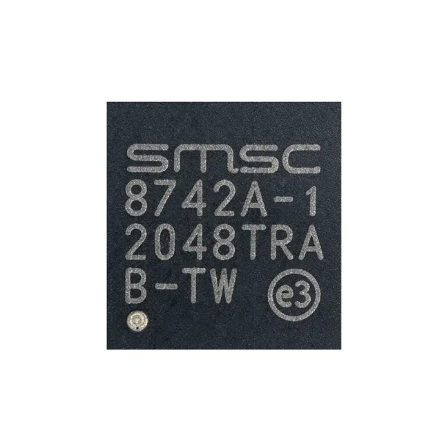
LAN8742A-CZ-TR - 10/100 Ethernet PHY, RMII, 24-SQFN | Microchip
The Microchip LAN8742A-CZ-TR is a low-power 10BASE-T/100BASE-TX Ethernet PHY transceiver with variable I/O voltage, packaged in a 24-pin SQFN (4x4 mm) and supplied on tape and reel. It supports MII and RMII MAC interfaces, operates from a 1.8V to 3.3V variable I/O supply, and is IEEE 802.3 / 802.3u compliant. The device integrates auto-negotiation, auto-polarity correction, and HP Auto-MDIX, eliminating the need for crossover cables. It is well-suited for consumer, embedded, and industrial Ethernet applications. A PHY (physical layer transceiver) is a key element of any Ethernet link: it sits between the MAC controller and the magnetic transformer/RJ-45, handling line encoding/decoding, link training, and electrical signaling over twisted-pair copper. PHY transceivers are part of the broader category of Ethernet interface ICs, which include MAC controllers, switches, and integrated MAC+PHY SoCs. The LAN8742A specifically implements the 10/100 Mbps copper PHY only; higher-speed Gigabit (1000BASE-T) PHYs use multi-level signaling (PAM) and more pins. Key features of the LAN8742A-CZ-TR include Wake-On-LAN support for system-level sleep modes, cable diagnostics for fault detection, and flexPWR flexible power technology for low-power operation. The variable I/O voltage (1.8V-3.3V) allows direct connection to low-voltage MCUs without level shifters. The HP Auto-MDIX feature automatically detects and compensates for TX/RX pair swaps, allowing either straight-through or crossover cables to be used interchangeably. Architecturally, the LAN8742A employs DSP-based echo and crosstalk cancellation to achieve robust 100BASE-TX performance over Cat5 cable. The on-chip PHY includes an integrated termination network and uses energy detect plus power-down modes to meet modern standby-power requirements. MII and RMII MAC interfaces are selectable via strap pins, allowing the same part to be paired with virtually any MCU or SoC MAC. Typical applications include IoT gateways, industrial Ethernet nodes, embedded web servers, building automation controllers, IP cameras, and consumer electronics requiring a wired network connection. The wide 1.8V-3.3V I/O range and low power consumption also make it attractive for battery-powered Ethernet-enabled devices. When designing with the LAN8742A-CZ-TR, follow the Microchip LAN8742 QFN Routing Checklist for proper PCB layout - the analog ground plane and 50-ohm impedance-controlled differential pairs are critical for radiated emissions and signal integrity compliance. Decoupling capacitors must be placed adjacent to each power pin, and the magnetics must be specified to IEEE 802.3 isolation and return-loss specifications. This page synthesizes distributor pricing, drop-in same-BLAN alternatives, and Microchip application-note design notes not found in the manufacturer datasheet alone - giving engineers a single, decision-ready reference.

LAN9252/ML - 2/3-Port EtherCAT Slave Controller, Dual PHY | Microchip
The Microchip LAN9252/ML is a 2/3-port EtherCAT slave controller (ESC) with dual integrated 100BASE-TX Ethernet PHYs, supplied in a 64-pin QFN (9x9 mm) package. It supports 100 Mbps full-duplex Ethernet, HP Auto-MDIX, optional 100BASE-FX fiber via an external transceiver, SPI/SQI host interfaces, 3 FMMUs, 4 SyncManagers, and a Distributed Clock mechanism. The part is targeted at cost-effective EtherCAT slave designs and operates from a 1.8 V/2.5 V/3.3 V digital core supply plus a 3.3 V analog supply. An EtherCAT slave controller (ESC) is an application-specific integrated circuit that implements the EtherCAT slave protocol entirely in hardware, exposing process data and mailbox registers to a host microcontroller over a parallel or serial Process Data Interface (PDI). Within the industrial communication stack, ESCs sit below real-time Ethernet masters and above generic MCUs; the family hierarchy is ESC -> industrial Ethernet controller -> communication IC -> semiconductor. Compared with earlier solutions such as the Beckhoff ET1100, the LAN9252 integrates the physical layer and uses a smaller QFN package, simplifying board layout and reducing BOM cost. Key features include two embedded full-duplex 100BASE-TX transceivers with HP Auto-MDIX, an SPI/SQI host interface with Digital I/O modes of up to 16 bits, support for external 100BASE-FX fiber via a fiber transceiver, on-chip 3 FMMUs and 4 SyncManagers, distributed clocking, cable diagnostics, and integrated termination resistors. The device supports 8/16-bit and 32-bit host microcontrollers and provides extensive interrupt, GPIO, and LED status resources. Architecturally, the LAN9252 combines an EtherCAT IP core (Beckhoff-licensed) with two 100 Mbps Ethernet PHYs, hardware DPRAM, FMMU/SyncManager logic, and an SPI/SQI bus bridge on a single die. Power architecture is split between a 1.8 V/2.5 V/3.3 V digital core and a 3.3 V analog PHY rail, which allows the digital host MCU to operate from lower voltages while the analog side retains high signal integrity for 100BASE-TX signaling. The QFN-64 package provides a single exposed pad (EP) that must be soldered to a low-impedance ground plane for thermal and EMI reasons. Typical applications include EtherCAT digital I/O modules, servo/stepper drives, encoder feedback, robotics and CNC peripherals, sensor/actuator hubs, and industrial motor controllers that need deterministic real-time Ethernet communications. Designers usually pair the LAN9252 with a small Cortex-M-class MCU that runs the application firmware and reads/writes the process image through the LAN9252's SPI/SQI registers. When designing with the LAN9252, follow Microchip's LAN9252 Schematic Checklist closely: place the 49.9 ohm 1% pull-up on TXPA/TXPB to VDD33TXRX1, use a 25 MHz reference clock, place the magnetics close to the PHY pins, and provide an EEPROM for configuration. The 64-pin QFN exposed pad must be soldered to a continuous ground copper pour to meet thermal and EMI performance, and the SPI/SQI mode strap must be selected correctly at reset. This page synthesizes real distributor pricing, drop-in pin-compatible alternatives from the same Microchip LAN92xx family, and practical design notes distilled from the LAN9252 Schematic Checklist - content not bundled together in the manufacturer datasheet alone.

LAN9252I/PT - 2/3-Port EtherCAT Controller | Microchip
The Microchip LAN9252I/PT is a 2/3-port EtherCAT slave controller with dual integrated 10/100 Ethernet PHYs, 100BASE-TX operation, and a 64-pin TQFP exposed-pad package. It supports a synchronous device SPI/SQI host interface, HP Auto-MDIX, digital I/O mode, and an external fiber transceiver for 100BASE-FX. The controller includes 4K bytes of dual-port memory and three Fieldbus Memory Management Units for EtherCAT communication. An EtherCAT slave controller, or ESC, is a semiconductor that connects an embedded controller or industrial I/O module to an EtherCAT segment. The ESC processes EtherCAT frames, manages distributed clocks, provides dual-port memory for the host application, and controls network ports through integrated Ethernet PHYs. The LAN9252I/PT therefore combines an EtherCAT communication engine, two 100Mbps Ethernet physical layers, and host-side control in one device. The LAN9252 family supports full-duplex 100BASE-TX on both integrated Ethernet ports and HP Auto-MDIX, allowing direct-connect or crossover Ethernet cables. The SPI/SQI interface connects the ESC to an MCU or embedded processor, while digital I/O mode lets EtherCAT-master-controlled signals be monitored or driven through the device. The external-transceiver path also supports 100BASE-FX when fiber connectivity is required. The 64-TQFP-EP package provides a 10 mm by 10 mm land pattern with an exposed thermal pad. The /PT ordering suffix identifies the tray package option, while the I variant identifies the industrial temperature grade. Designers should confirm the exact electrical limits, pin names, timing values, recommended magnetics, and decoupling values against the manufacturer datasheet before releasing a PCB layout. Typical applications include distributed I/O modules, servo and motion-control nodes, PLC interfaces, industrial Ethernet gateways, robot control systems, and EtherCAT fieldbus equipment. The integrated PHYs reduce external Ethernet PHY count, while the ESC resources allow a host processor to exchange process data and mailbox information with the EtherCAT master. PCB implementation must preserve the package footprint and exposed-pad land pattern, provide adequate power and ground planes, route differential Ethernet pairs according to the datasheet guidance, and place magnetic-interface and decoupling components close to their associated pins. Verify isolation, magnetics, termination, and cable requirements for the target industrial installation. This page consolidates the verified manufacturer and distributor information, package and interface details, sourcing context, and design guidance for engineers evaluating the LAN9252I/PT. It is intended to accelerate BOM review and board-level planning while leaving unverified electrical parameters explicitly marked for confirmation against the manufacturer datasheet.
LAN9252TI/PT - 2/3-Port EtherCAT Slave Controller | Microchip
The Microchip Technology LAN9252TI/PT is a 2/3-port EtherCAT device controller (ESC) with dual integrated Ethernet PHYs, each containing a full-duplex 100BASE-TX transceiver supporting 100 Mbps operation. Housed in a 64-pin TQFP-EP (10x10 mm) package with an exposed thermal pad, it operates from 1.8 V/2.5 V/3.3 V supplies and presents a digital SPI host interface. The LAN9252TI/PT supports HP Auto-MDIX and exposes two or three Ethernet ports, enabling designers to build daisy-chain EtherCAT nodes without an external PHY. What is an EtherCAT slave controller? An EtherCAT Slave Controller is the silicon heart of a slave node on an EtherCAT fieldbus, which is a deterministic real-time Ethernet protocol widely used in industrial automation (Beckhoff's EtherCAT). The ESC handles the on-the-fly processing of Ethernet frames, manages distributed clock synchronization, and exposes process data via a host interface such as SPI or parallel bus to an application microcontroller. The LAN9252TI/PT is therefore a bridge IC: it is a slave on the EtherCAT network and a peripheral to a host MCU. It belongs to the wider category of industrial Ethernet controllers, complementing protocols such as PROFINET, EtherNet/IP and Modbus TCP. Key features include dual 100BASE-TX PHYs with HP Auto-MDIX, an SPI host interface for the application MCU, 2/3 port switch capability, integrated 1.8 V/2.5 V/3.3 V I/O tolerance, hardware cable diagnostics and an industrial temperature range. The integrated PHYs eliminate two external transceiver ICs and the associated magnetics design, while Auto-MDIX allows direct or crossover cables interchangeably. Three ports enable line, ring or star network topologies natively on the chip. Architecturally, the LAN9252TI/PT pairs an EtherCAT IP core (Beckhoff-licensed ET1100-equivalent logic) with two 100 Mbps Ethernet PHY macros and a digital SPI/parallel bridge. The device supports distributed clocks (DC) with sub-microsecond synchronization, FMMU, SyncManager and watchdog functions defined by the EtherCAT specification. Internal FIFOs decouple EtherCAT traffic from the host MCU, allowing a low-cost MCU to control a high-performance fieldbus. Typical applications include servo/stepper drives, I/O modules, sensors and actuators on EtherCAT networks, programmable logic controllers (PLC) sub-modules, robotics joint controllers and CNC axes. Industrial designers value the LAN9252TI/PT because it shrinks a complete 2-port EtherCAT slave - including magnetics and termination - onto a small PCB that talks to a low-cost SPI MCU. Designers should route the 100BASE-TX differential pairs as controlled-impedance (100 ohm differential) traces and connect the center tap of each transformer through the integrated termination resistors. The exposed thermal pad must be soldered to a sufficient copper pour to dissipate the roughly 0.5-1 W typical dissipation under 100 Mbps full-duplex operation. DC and ripple on each analog supply pin must be kept below 50 mVpp to maintain EtherCAT conformance. This page consolidates distributor pricing, drop-in alternatives, and engineering design notes that go beyond what the manufacturer datasheet provides, including same-family Microchip options and cross-brand EtherCAT competitor context.

LAN9255-I/ZMX019 - EtherCAT Slave Controller + Cortex-M4F MCU | Microchip
The Microchip Technology LAN9255-I/ZMX019 is a 2/3-port EtherCAT device controller (ESC) System-In-Package (SIP) integrating dual 100BASE-TX Ethernet PHYs, the Microchip LAN9253 ESC, and the Microchip SAM E53J ARM Cortex-M4F MCU into a single 128-pin TQFP (14x14 mm) package. It supports 100 Mbps (100BASE-TX) full-duplex communication, includes 512 kB of integrated MCU memory, and offers USB 2.0 plus RMII host interfaces for broad system connectivity. An EtherCAT slave controller is a specialized industrial-Ethernet IC that offloads the EtherCAT protocol stack (originally developed by Beckhoff Automation) from the host processor, allowing deterministic sub-cycle communication on standard 100BASE-TX cabling. EtherCAT belongs to the industrial-Ethernet protocol family alongside PROFINET, EtherNet/IP, and SERCOS, and is governed by the ETG (EtherCAT Technology Group). Within the broader hierarchy, the LAN9255 sits as an Industrial Communication IC -> Network Controller -> Semiconductor. Integrating the PHY, ESC, and application MCU into one SIP reduces board area, simplifies EMC design, and removes the need for an external host MCU in cost-sensitive slave designs. Key features of the LAN9255-I/ZMX019 include three EtherCAT ports (Port 0, Port 1, and a cascaded/loopback Port 2), integrated dual 100BASE-TX PHYs that eliminate external magnetics interfacing complexity, USB 2.0 Full-Speed (12 Mbps) device port, RMII interface for an external host MCU if desired, on-chip Cortex-M4F MCU with FPU for application code, hardware offload of EtherCAT mailbox and process-data handling, and industrial-grade -40 C to +85 C operation. The 128-TQFP package is lead-free and RoHS compliant for global industrial deployment. The LAN9255 architecture combines Microchip's proven LAN9253 ESC IP with the SAM E53J ARM Cortex-M4F microcontroller, enabling stand-alone EtherCAT slave designs. The dual integrated PHYs each provide full-duplex 100BASE-TX transceivers with HP auto-MDI/MDIX, removing the need for two external PHY ICs. Distributed clocks and cable redundancy features are handled in hardware, ensuring deterministic communication for servo, motion, and I/O applications. The device works with the MPLAB Harmony EtherCAT Slave Stack and Microchip's EVB-LAN9255 evaluation platform. Typical applications for the LAN9255-I/ZMX019 include EtherCAT servo drives, distributed I/O modules, stepper motor controllers, sensor and encoder EtherCAT slaves, hydraulic valve drivers, and industrial robot subsystems. The integrated MCU + dual-PHY combination is particularly attractive for designers building minimum-BOM EtherCAT slaves without a separate host processor. When designing with this part, ensure the 128-TQFP thermal pad is soldered to a substantial ground copper pour for heat extraction and signal-integrity performance. Use Microchip's AN-DS LAN9255 PHY layout guidelines for proper Ethernet magnetics and RJ45 interface. The integrated MCU eliminates the need for an external application processor in many designs, simplifying BOM cost. This page synthesizes distributor pricing, drop-in alternatives, and application-focused design guidance that goes beyond what the LAN9255 datasheet (Microchip document 00003646B) covers alone.

LAN9255-V/ZMX020 - EtherCAT Slave Controller with MCU | Microchip
The Microchip Technology LAN9255-V/ZMX020 is a 2/3-port EtherCAT Device Controller with integrated dual 100BASE-TX PHYs and an integrated SAM E53J 32-bit ARM Cortex-M4F MCU, packaged in a 128-pin TQFP-EP (14x14 mm) with exposed thermal pad. It combines an EtherCAT slave controller, two Ethernet PHYs, and an application microcontroller in a single System-In-Package (SiP), eliminating the need for an external MCU on simple EtherCAT slave node designs. An EtherCAT slave controller (ESC) is a specialized industrial-Ethernet IC that implements the Beckhoff EtherCAT slave protocol on the device side of an EtherCAT network. EtherCAT is a deterministic real-time Ethernet standard used for synchronized motion control, I/O, and drive communication in factory automation. The ESC sits below the EtherCAT master and the standard Ethernet/IP stack in the network hierarchy and works alongside general industrial controllers like PLCs and motion controllers. Key features of the LAN9255-V/ZMX020 include dual integrated 100BASE-TX Ethernet PHYs supporting 100 Mbps full-duplex, a 3-port EtherCAT switch fabric supporting daisy-chain and ring topologies, USB 2.0 FS device/host interface, RMII for external PHY connection, SPI/QSPI for host communication, and 1024 KB of integrated Flash and 256 KB SRAM inside the SAM E53J MCU die. The integrated MCU is pre-flashed with a bootloader and can run application code for simple slaves, removing external processor overhead. The device is designed for high-volume industrial EtherCAT slave applications where board space, BOM cost, and deterministic cycle time are critical. Typical cycle times below 62.5 µs are achievable through hardware FMMU, SyncManager, and DC (Distributed Clocks) engines. Typical applications include EtherCAT digital and analog I/O modules, servo drives and stepper motor drivers, robotics servo nodes, sensor hubs, encoder interfaces, and other industrial automation peripherals. The dual PHY + MCU integration makes it ideal for compact, low-cost slaves with on-board intelligence. When designing with the LAN9255, ensure proper 25 MHz reference oscillator quality for jitter compliance, route the MII/RMII traces as 50-ohm controlled impedance, and place the decoupling capacitors as close to the supply pins as possible. The exposed thermal pad must be soldered to a sufficient copper pour for thermal dissipation. This page synthesizes distributor pricing across 9 channels, true drop-in alternatives in the same 128-TQFP-EP footprint, and practical design notes not found in the manufacturer datasheet, giving engineers a single source for selection, sourcing, and integration.

LAN9500A-ABZJ - Hi-Speed USB 2.0 to 10/100 Ethernet Bridge | Microchip
The Microchip LAN9500A-ABZJ is a single-chip Hi-Speed USB 2.0 to 10/100 Ethernet bridge controller integrating a USB 2.0 PHY, USB 2.0 device controller, 10/100 Ethernet MAC, 10/100 Ethernet PHY, TAP controller, EEPROM controller, and FIFO controller in a compact 56-pin QFN (8x8 mm) package. The device implements Control, Interrupt, Bulk-in, and Bulk-out USB endpoints and is compliant with the USB 2.0 Hi-Speed standard, providing 480 Mbps upstream connectivity to a host processor. An Ethernet bridge controller is a semiconductor device that translates between two dissimilar network or bus protocols, presenting one physical interface to the host system and another to the network. In this product's case, the bridge maps USB 2.0 bulk transfers to IEEE 802.3/802.3u Ethernet frames, allowing any embedded host with a USB port to add wired Ethernet without a native MAC. The bridge belongs to the broader hierarchy: USB-to-Ethernet bridge -> network interface controller -> Ethernet controller -> interface IC -> integrated circuit. Key features include integrated HP Auto-MDIX for automatic cable polarity correction, auto-negotiation per IEEE 802.3u, flexible address filtering with a 48-bit perfect address, 64 hash-filtered multicast addresses, and a TAP controller for diagnostic packet capture. The on-chip PHY embeds ±8 kV HBM and ±15 kV air discharge ESD protection, which eliminates external TVS arrays on the magnetics lines and shrinks BOM cost in cost-sensitive designs. The LAN9500A is built on a low-power CMOS process and operates from three internal rails (1.2 V, 2.5 V, 3.3 V) generated from a single 3.3 V supply. Reduced power operating modes plus an EEPROM-less design option help reduce overall system BOM and standby current. An external MII interface allows connection of an additional external PHY for dual-port or fiber applications, although most designs use the integrated PHY. Typical applications include USB-to-Ethernet dongles, embedded Linux/Windows single-board computers, industrial controllers needing network connectivity, set-top boxes, printers with network ports, and USB port-replicators. The integrated PHY and USB PHY make it ideal where board area is constrained but full 10/100 throughput is required. When designing with this device, ensure the 25 MHz crystal meets the datasheet's ±50 ppm tolerance and load capacitance specification. Use a 1 Mbit/s Ethernet magnetics module with a 1:1 turns ratio, and follow Microchip's reference schematic for the EXRES resistor value, which differs from the original LAN9500 part. This page consolidates distributor pricing from DigiKey and Mouser, three verified same-brand drop-in alternatives from Microchip's LAN95xx family, and PCB design notes not present in the standalone datasheet PDF.

LAN9500A-ABZJ-TR - USB 2.0 to 10/100 Ethernet Controller | Microchip
The Microchip Technology LAN9500A-ABZJ-TR is a Hi-Speed USB 2.0 to 10/100 Ethernet controller IC that integrates a USB 2.0 device controller, USB PHY, 10/100 Ethernet MAC, and 10/100 Ethernet PHY into a single chip, housed in a 56-pin QFN (8x8 mm) package with exposed pad. It supports USB 2.0 Hi-Speed (480 Mbps), 10Base-T and 100Base-TX Ethernet, HP Auto-MDIX, and provides an external MII interface for connecting an additional PHY. A USB-to-Ethernet controller is a bridge IC that converts USB transactions from a host processor into Ethernet frames on a network. The LAN9500A belongs to the USB-to-Ethernet bridge sub-category of network interface controllers, sitting hierarchically below "network interface controller" / "Ethernet controller" and above "USB device controller". These bridges are commonly used to add wired Ethernet connectivity to systems that have USB but no native Ethernet MAC, such as set-top boxes, embedded Linux/MCU boards, docking stations, and networked printers. Key features include USB 2.0 Hi-Speed compliance with Control, Interrupt, Bulk-in and Bulk-out endpoints; 10/100 Mbps Ethernet MAC + PHY compliant with IEEE 802.3 and IEEE 802.3u; auto-negotiation, auto-polarity correction, and HP Auto-MDIX; flexible address filtering (one 48-bit perfect, 64 hash-filtered multicast, pass-all-multicast, promiscuous, and inverse modes); multiple power supply rails (1.2V, 2.5V, 3.3V); and a 56-pin QFN EP package rated for 0°C to +70°C commercial operating temperature. Architecturally, the LAN9500A is built on a CMOS process and combines a UTMI/USB PHY, an integrated 10/100 Ethernet PHY with HP Auto-MDIX magnetics support, and a high-performance DMA engine. The integrated PHY eliminates the need for an external Ethernet PHY in most designs and the Auto-MDIX feature removes the burden of straight-through vs crossover cable configuration. Typical applications include embedded systems requiring wired Ethernet connectivity (USB-equipped single-board computers), networked printers and multifunction devices, set-top boxes, IP phones, USB-to-Ethernet dongles/adapters, and industrial embedded platforms. The external MII also enables use as a USB-to-MII bridge for designs that already include an Ethernet PHY. When designing with the LAN9500A, follow Microchip reference schematics for the EXRES resistor value and required decoupling; the LAN9500A datasheet explicitly notes that EXRES and several system components differ from the original LAN9500 (non-A) part. Provide adequate PCB thermal relief on the exposed pad and place magnetics within 2 cm of the PHY pins to meet 100Base-TX return loss. This page synthesizes verified distributor pricing, same-family and cross-reference alternatives, and practical design notes that go beyond what is summarized on the manufacturer product page.

LDA505 - Inductive Proximity Switch Driver IC, SOP-16 | TCA505 Pin-Compatible
The LDA505 is an application-specific bipolar integrated circuit housed in a 16-pin Small Outline Package (SOP-16), designed as a functional drop-in equivalent for the Infineon/Siemens TCA505 in inductive proximity switch applications. The device operates over an industrial temperature range of -65°C to +150°C and integrates short-circuit protection on its output stage, making it well-suited for harsh industrial sensor environments. It is marketed by Chinese semiconductor vendors as a pin-compatible alternative when the original TCA505 is in short supply or allocated. An inductive proximity switch driver IC is a specialized interface circuit that conditions the signal from an inductive sensor coil (typically an LC oscillator) and converts it into a clean digital logic output. In the broader system hierarchy it sits between the sensing element (the LC tank or oscillator) and the host controller (a PLC input card, microcontroller GPIO, or industrial counter module). Because the LDA505 integrates the rectifier, threshold detector, hysteresis block, and output driver in one chip, designers replace a discrete solution of dozens of parts with a single IC. Category synonyms include 'proximity sensor IC', 'inductive switch ASIC', and 'proximity amplifier IC'. The defining features of the LDA505 are its bipolar process technology for robust output drive, integrated short-circuit / overload protection on the output pin, wide supply tolerance compatible with 24 V industrial rails, and SOP-16 footprint that exactly matches the TCA505 land pattern. These features allow direct PCB-level substitution without board rework, provided the host MCU's input logic threshold is verified. Architecturally the device contains a built-in rectifier for the AC-coupled inductive sensor signal, a comparator with programmable hysteresis, a voltage regulator for internal biasing, and a push-pull or open-collector output stage protected against sustained shorts to VCC or GND. Designers should review the device marking versus the TCA505 to confirm compatibility because some revisions differ in output polarity. Typical applications include industrial 24 V inductive proximity sensors, position detectors on conveyor lines, metal-object counters, machine-tool end-of-travel limits, and automotive gear-position sensors. The integrated short-circuit protection also makes the part attractive in safety-oriented designs where wire shorts in the field are a real risk. When designing with the LDA505, treat the supply rail as a 24 V industrial bus with proper reverse-polarity and TVS protection on the connector. Bypass the supply pin with a 100 nF ceramic close to the IC and add a 10 µF bulk capacitor if the cable run exceeds 1 m to suppress load-dump transients. This page consolidates distributor pricing, drop-in equivalents, and practical design considerations for the LDA505 that are not found in any single vendor datasheet.

LICAL-DEC-MS001-TI 8-Button Remote Decoder | TE Conn
The TE Connectivity LINAL-DEC-MS001-TI is an MS Series data-decoder integrated circuit for remote-control systems, supporting the status of up to eight buttons or contacts and supplied in a 20-SSOP surface-mount package. The verified listing identifies a 2.0 V to 5.5 V analog supply range, while the target suffix indicates the TI distributor ordering code associated with the LINAL-DEC-MS001 device. A remote-control decoder is a logic IC that receives encoded button or contact information and translates it into digital outputs or status signals for a host controller. In the broader electronics hierarchy, it belongs to interface ICs rather than a general-purpose microcontroller: the decoder handles a defined remote-control protocol or input structure while leaving system-level decisions to another controller. This makes it useful in alarm systems, communication systems, access controls, and other products requiring compact button-state decoding. Verified product information identifies the LINAL-DEC-MS001 as a 20-SSOP device with a 5.30 mm package width. The MS Series is intended for remote-control applications where multiple button or contact states must be transferred reliably into a digital system. The exact logic levels, timing, current consumption, operating temperature, output format, and supported channel count beyond the verified eight-button description are not supplied in the retrieved data and must be confirmed from the manufacturer documentation before design release. The part is particularly relevant to systems that already use the MS Series remote-control architecture. Designers should verify the encoder family pairing, signal polarity, supply tolerance, and timing requirements before committing the IC to a new PCB. A decoder can reduce host-controller input count by presenting multiple remote-control states through a defined interface, but incorrect protocol assumptions can prevent valid operation even when the package and supply requirements appear compatible. Typical uses include alarm-system panels, communication equipment, industrial remote controls, and embedded control interfaces. Keep the 20-SSOP footprint and pin mapping compatible with the manufacturer drawing, provide the required bypass capacitors near the supply pins, and validate signal conditioning at the receiver. The retrieved distributor listings support procurement comparison, but pricing and lead time must be refreshed at the time of quotation. This page consolidates the verified manufacturer and distributor information, separates known specifications from missing parameters, and provides engineering-oriented design guidance. It does not invent pin functions, timing values, or lifecycle claims that are not present in the supplied evidence.

LM111 - High-Speed Differential Comparator | Texas Instruments
The Texas Instruments LM111 is a single high-speed differential voltage comparator with open-collector and open-emitter outputs, designed for operation from a single 5 V supply through dual ±15 V supplies. Its stated maximum input bias current is 300 nA, maximum input offset current is 70 nA, and the device includes strobe capability for controlled comparator operation. The LM111 is packaged in an 8-pin TO-99 style metal can package. A voltage comparator is an analog integrated circuit that compares two input voltages and produces a digital logic state indicating which input is higher. The LM111 belongs to the comparator category within analog and interface ICs, and its differential inputs make it useful for threshold detection, signal conditioning, timing, and control systems. Unlike an operational amplifier intended primarily for linear amplification, the comparator is optimized for rapid state changes and logic-level output compatibility. The LM111, LM211, and LM311 family is designed around a wide supply-voltage range, including ±15 V operational-amplifier supplies and 5 V logic systems. The output levels are compatible with many TTL and MOS circuits, allowing the LM111 to bridge analog sensing and digital control. Its differential input arrangement supports sensing a small difference between two voltages while presenting a logic result to downstream circuitry. The LM111 family also includes related temperature grades and device variants. Texas Instruments states that the LM111-N has the same pin configuration as the LM106 and LM710, while the LM211-N and LM311-N provide different specified temperature ranges. The exact LM111 pin configuration and electrical limits must be confirmed against the applicable manufacturer datasheet and package variant before production release. Typical applications include line and threshold comparators, pulse and window detection, level translation into TTL or MOS logic, industrial control interfaces, analog signal conditioning, and legacy instrumentation. Because the output is open collector or open emitter, a pull-up or pull-down load resistor is generally required at the output. This architecture can provide wired logic behavior and flexible output interfacing, but it also makes pull-device selection and output speed part of the system design. When selecting a replacement, verify the package, pinout, supply limits, input offset and bias behavior, response time, output topology, and temperature grade. The verified material supports the LM111 identity and family-level characteristics, but it does not provide enough verified information here to reproduce every electrical limit or package drawing. This page therefore distinguishes documented values from parameters requiring confirmation rather than guessing them.
LM211-LM311 - Single High-Speed Differential Comparator
The Texas Instruments LM211-LM311 is a family designation for the LM211 and LM311 single high-speed differential comparators, designed for wide supply ranges from single 5 V operation through ±15 V split supplies. The LM211 and LM311 provide low input currents and open-collector outputs intended for driving lamps, relays, and logic-compatible loads. Their differential inputs can accept voltages outside the supply rails, while the output polarity and output-current requirements determine the external pull-up arrangement. A voltage comparator is a semiconductor device that compares two input voltages and switches its output according to their relationship. In the broader IC hierarchy, a comparator belongs to the analog signal-conditioning and interface family, alongside op-amps and logic interfaces. The LM211-LM311 family is useful when a design needs a threshold decision, overvoltage indication, level translation, or relay-drive function rather than linear analog amplification. The verified manufacturer material identifies the devices as single high-speed comparators with low input current. According to the Texas Instruments datasheet material supplied, the output levels are compatible with most TTL and MOS circuits, and the devices are capable of driving lamps or relays. The onsemi material additionally states that the inputs can be isolated from system ground while the output can drive loads referenced to ground, VCC, or VEE. These features support industrial control, instrumentation, and legacy interface designs. The family includes temperature and sourcing differences between LM211 and LM311 variants. The supplied Mouser datasheet excerpt specifies LM211 operation from −25°C to +85°C and LM311 operation from 0°C to +70°C for the referenced comparison. The same excerpt states that offset voltage, offset current, and bias-current specifications apply from a single 5 V supply up to ±15 V supplies, and that the positive input voltage limit is 30 V above the negative supply. Exact ordering codes and package-specific electrical limits require the relevant manufacturer datasheet and suffix. Typical uses include sensing a control voltage against a reference, detecting an overvoltage condition, switching a relay when a sensor crosses a threshold, and interfacing an analog signal to TTL or MOS logic. Because the output is open collector, a pull-up resistor is generally required. The pull-up must be selected against the required sink current, output voltage, speed, and system supply constraints. The principal design consideration is ensuring that input common-mode voltage, supply voltage, output pull-up, and input/output isolation meet the particular LM211 or LM311 ordering variant. The family designation alone does not identify a unique package, suffix, temperature grade, or exact parameter set. Use the manufacturer datasheet linked on this page before committing a footprint or substituting a part. This page consolidates the verified manufacturer descriptions, practical comparator usage guidance, and the available cross-reference information. It distinguishes confirmed family-level facts from ordering-code-specific data that is not established by the supplied search results.

LMH1226RTWT - 12G UHD Dual-Output Reclocker | Texas Instruments
The Texas Instruments LMH1226RTWT is a low-power dual-output 12G UHD reclocker supporting SMPTE video rates up to 11.88 Gbps and 10 GbE video over IP, housed in a 24-pin WQFN (4x5 mm) package. Typical power consumption is 214 mW, dropping to 16 mW in the absence of an input signal. A reclocker is a signal-conditioning device in the serial-digital-video signal chain: it extracts the clock from a degraded incoming data stream and retransmits the data with a clean, jitter-free clock, effectively regenerating the signal. Reclockers sit within the broader hierarchy of video interface ICs under linear/video processing semiconductors, bridging cable equalizers and cable drivers in broadcast and professional AV equipment. Key features include support for SMPTE data rates up to 11.88 Gbps (12G-SDI), 10 Gigabit Ethernet over IP, DVB-ASI, and AES10 (MADI) protocols. An adaptive board-trace equalizer at input IN1 is SFF-8431 compatible and handles both SMPTE and 10 GbE rates. The dual output drivers provide programmable de-emphasis to compensate board trace losses at the outputs. The reclocker attenuates high-frequency jitter to deliver the best signal integrity for Ultra HD 4K/8K video transport. With typical power consumption of only 214 mW and 16 mW in signal-absent mode, it suits dense, power-sensitive broadcast designs. The device is configured through SPI, and its high input jitter tolerance allows operation with degraded or long-reach incoming signals. Typical applications include 12G-SDI broadcast cameras and switchers, UHD video routers, 4K/8K video-over-IP infrastructure, and signal distribution amplifiers in professional AV systems. A key design consideration: the LMH1226 is pin compatible with the LMH1219 (a 12G-UHD cable equalizer with integrated reclocker), allowing PCB footprint reuse when a design needs equalization ahead of the reclocker. This page synthesizes distributor pricing context, pin-compatible alternatives, and practical design notes not found in the manufacturer datasheet.
LSF0101 - 1-Bit Auto-Bidirectional Level Translator | Texas Instruments
The Texas Instruments LSF0101 is a single-channel auto-bidirectional multi-voltage level translator for open-drain and push-pull applications, housed in an ultra-compact 6-X2SON (1 x 0.8 mm) package. It translates between voltage domains without a direction pin, minimizing system design effort for buses such as PMBus, I2C, and SMBus. A level translator (also called a voltage shifter or logic-level converter) is an interface IC that safely connects circuits operating at different supply voltages - for example a 1.8 V microcontroller communicating with a 3.3 V or 5 V peripheral. Level translators belong to the broader voltage translator / logic IC hierarchy within interface semiconductors, and the LSF0101 is the smallest, single-bit member of the TI/Nexperia LSF family. Key features include automatic bidirectional operation with no DIR control signal, up-translation of up to 100 MHz and down translation of 100 MHz or more at a capacitive load of 30 pF or less, and 5 V tolerant I/O pins for TTL compatibility. According to the TI and Nexperia datasheets, the pass-gate (NFET) switch architecture delivers very low propagation delay and supports both open-drain two-wire buses and push-pull interfaces. The reference-bias topology (VREF_A / VREF_B) defines the two voltage domains; the low-side reference is applied through the EN pin bias network and an analog pass switch connects the A and B pins. This makes the LSF0101 especially suitable for two-wire buses where direction changes asynchronously - something buffered push-pull translators cannot handle without a direction input. Typical applications include I2C, SMBus, and PMBus level shifting, 1.8 V to 3.3 V or 5 V mixed-voltage MCU peripherals, industrial control buses, and mobile or wearable designs where the 1 x 0.8 mm X2SON footprint conserves board area. Design consideration: the LSF family requires correct pull-up resistor sizing on open-drain buses to meet rise-time targets; the reference-side bias resistor (typically 200 kohm per TI datasheet guidance) sets translation speed, so verify its value against bus capacitance and data rate before production.

LSF0108PWR - 8-Ch Bidirectional Level Translator | TI
The Texas Instruments LSF0108PWR is an 8-channel auto-bidirectional multi-voltage level translator for open-drain and push-pull applications, housed in a 20-pin TSSOP (PW) package. Both A-side and B-side ports support 0 V to 5 V, with approximately 1.5 ns propagation delay, making it suitable for I2C, SMBus, UART, and SPI interfaces. A voltage level translator is an interface IC that lets digital signals in different voltage domains communicate safely by shifting signal levels as they pass between two logic families. Within the system hierarchy, a level translator is a type of logic interface IC within the broader integrated circuits category. The LSF0108 uses a pass-gate (series MOSFET) architecture with external pull-up resistors, providing automatic direction sensing without a direction-control pin. Key features include bidirectional translation without a direction pin, support for both open-drain and push-pull drivers, and an operating temperature range of -40C to +125C. The LSF family covers the 0.95 V to 5 V translation range, spanning nearly all common logic levels (1.2V, 1.8V, 2.5V, 3.3V, 5V). Low standby current and the compact TSSOP-20 footprint suit space-constrained mixed-voltage boards. Technically, each channel employs a series pass transistor. Direction is determined automatically by whichever side drives, eliminating direction-control signals and simplifying firmware. The reference side (VREF_A or VREF_B) sets the lower voltage domain; pull-up resistors on the opposite side set the higher domain. Typical applications include I2C bus level shifting between 1.8V and 3.3V or 5V domains, UART interfacing between microcontrollers and peripherals, SPI communication between different logic voltages, and mixed-voltage sensor or memory interfaces. Design tip: size external pull-up resistors according to bus capacitance and target speed (1-10 kOhm for 400 kHz I2C). Correct VREF sequencing at power-up is essential; refer to TI datasheet SCPS229 for power-up requirements.
LSF0108QPWRQ1 - Auto 8-Ch Bidirectional Level Shifter | TI
The Texas Instruments LSF0108QPWRQ1 is an automotive-grade, 8-channel bidirectional multi-voltage level translator for open-drain and push-pull applications. It translates between voltage domains from 0.95V to 5V without a direction pin, housed in a 20-pin TSSOP (PW) package and rated for -40C to +125C operation per AEC-Q100. A level translator, or voltage level shifter, is an interface IC that enables digital communication between circuits operating at different supply voltages. It sits between a low-voltage controller, such as a 1.8V MCU, and a higher-voltage peripheral, such as a 3.3V sensor, ensuring logic levels are interpreted correctly. Level translators belong to the broader interface IC family, and the LSF family uses a pass-gate (N-MOSFET) architecture with external pull-up resistors, allowing automatic bidirectional translation without direction control. Key features include bidirectional operation with no direction pin, voltage support from 0.95V to 5V, and compatibility with both open-drain buses like I2C and push-pull signals. The device supports up to 100 MHz up-translation and greater than 100 MHz down-translation at <=30 pF load, and 40 MHz up/down translation at 50 pF load, per the TI datasheet (Rev. H). Technically, each channel uses a single N-channel MOSFET with external pull-ups defining the high level on each side. When either side drives low, the MOSFET conducts and pulls the opposite side low through the resistor network, enabling automatic bidirectional shifting. This removes GPIO overhead for direction signaling and simplifies firmware in multi-voltage systems. Typical applications include automotive body control modules, infotainment systems, MDIO management buses, and sensor interfaces where 1.8V, 2.5V, 3.3V, and 5V domains coexist, plus industrial automation mixed-voltage links. Design tip: select pull-up resistor values according to bus capacitance and speed; lower values improve edge rates but raise current consumption, and VREF pins must be tied to the respective rails to set translation levels correctly.

LSF0204RUTR - 4-Bit Bidirectional Level Translator | Texas Instruments
The Texas Instruments LSF0204RUTR is a 4-bit bidirectional multi-voltage level translator for open-drain and push-pull interfaces, housed in a 12-pin UQFN (RUT) package measuring 1.7 mm x 2.0 mm. The device operates with Vref_A from 0.8 V to 4.5 V and Vref_B from 1.8 V to 5.5 V, supporting bidirectional translation between any voltages from 0.8 V to 5.0 V without a direction pin. Typical data-rate capability exceeds 100 MHz in push-pull mode, making it suitable for SD card, SIM card, I2C, SPI, GPIO, and UART bridging. A bidirectional voltage level translator (also called a level shifter or logic-level translator) is an interface IC that connects two logic domains operating at different supply voltages. The LSF0204 belongs to the broader category of voltage translators, which are themselves a sub-category of interface ICs used in mixed-voltage digital systems. Because modern SoCs, microcontrollers, and sensors frequently operate at voltages other than 5 V (1.8 V, 3.3 V, 1.2 V), translators are essential glue logic that prevents damage and signal-integrity problems when devices of different voltage domains must communicate. Key features of the LSF0204 include 4 channels per package, support for both open-drain (I2C-style) and push-pull (SPI, GPIO) topologies, automatic direction sensing without a DIR pin, and an operating temperature range of -40 °C to +125 °C. The wide voltage range combined with auto-bidirectional operation eliminates the firmware burden of direction control and reduces BOM cost by removing external pull-up/down components on most paths. The compact UQFN-12 footprint is well-suited for space-constrained wearables, mobile devices, and IoT modules. Architecturally, the LSF0204 uses TI's pass-gate-based translator topology with internal one-shot accelerators that improve rise/fall time when driving capacitive bus loads. This edge-rate enhancement enables clean signals at higher bus speeds than a pure passive FET translator, while still drawing minimal quiescent current. The part supports hot-insertion because both reference rails can be ramped independently, and Ioff (partial-power-down) protection prevents back-feeding when either rail is off. Typical applications include SD card level shifting between a 1.8 V host SoC and a 3.3 V card, I2C bus translation in multi-voltage sensor hubs, SPI bridging between a low-voltage MCU and 5 V peripherals, SIM/UIM card interfaces, and general-purpose GPIO expansion across voltage domains. The wide voltage window makes it equally well-suited for legacy 5 V systems and modern sub-2 V processors. When designing with the LSF0204, the engineer should observe one practical rule: pull-up resistors are required on each side for open-drain buses (I2C), with values selected to meet the rise-time budget of the target bus speed; push-pull signals do not require pull-ups but the reference rails must both be present for reliable operation. Place both Vref_A and Vref_B decoupling capacitors within 2 mm of the IC pins. This page synthesizes distributor pricing, verified drop-in alternatives, and practical design notes not found in the manufacturer datasheet alone.

LTC1067IGN - Dual Switched-Cap Filter 20kHz | Analog Devices
The Analog Devices LTC1067IGN is a rail-to-rail, very low noise universal dual switched-capacitor filter building block that delivers two independent 2nd-order filter sections with cutoff frequencies up to 20 kHz in a 16-pin SSOP (narrow) package. Each filter section uses external resistors and the internal switched-capacitor architecture to implement low-pass, band-pass, notch, and all-pass responses. The device targets signal-conditioning applications where small footprint, low noise, and high dynamic range are mandatory. What is a switched-capacitor filter? A switched-capacitor filter is an active filter topology that emulates a resistor using a capacitor switched at a clock frequency, allowing precise, monolithic filter implementations without external precision capacitors. Within the broader IC taxonomy, switched-capacitor filters fall under active filters -> analog filters -> signal conditioning -> analog ICs -> semiconductors. They are preferred over continuous-time active filters for applications requiring tight frequency accuracy relative to an external clock. Key features include a clock-to-cutoff ratio of 100:1 (the LTC1067-50 variant uses 50:1), rail-to-rail input and output swing that maximizes dynamic range on low-voltage supplies, 60 dB signal-to-noise ratio, and a low noise floor suitable for instrumentation-grade signal chains. Each second-order block uses five external resistors, allowing independent configuration as a low-pass, high-pass, band-pass, or notch stage. Two blocks can be cascaded externally to build a 4th-order filter. The architecture is built on Analog Devices' precision switched-capacitor technology with CMOS analog switches and on-chip clock generation. The clock input accepts a TTL or CMOS external source, and the internal master clock divider sets the filter cutoff, simplifying design-in when synchronization to a system clock is required. The dual-block topology also enables independent filtering of two channels, such as stereo audio or dual-axis sensor signals, in a single IC. Typical applications include antialiasing filters for 16-bit ADCs, smoothing filters for DAC outputs, dual-channel audio crossover networks, instrumentation low-pass filters in data acquisition systems, and ultrasonic transducer front-end filtering in medical imaging. The wide dynamic range makes the LTC1067IGN particularly attractive when the upstream signal already spans most of the supply range. When designing with this part, plan clock-to-cutoff ratio carefully: the cutoff frequency equals fCLK/100 (or /50 for the -50 variant). A stable, low-jitter clock is essential - phase noise on the clock translates directly into passband distortion. Keep clock traces short and away from analog signal traces to prevent coupling. This page synthesizes distributor pricing, pin-compatible drop-in alternatives, and practical design notes that go beyond the manufacturer datasheet's typical application circuits.

LTC2846IG - 3.3V Multiprotocol Transceiver w/ Termination | Analog Devices
The Analog Devices LTC2846IG is a 3-driver/3-receiver multiprotocol transceiver with on-chip cable termination, housed in a 36-pin SSOP (Industrial Grade) package. Operating from a single 3.3V supply, it supports software-selectable protocols including RS232, RS449, EIA530, EIA530-A, V.35, V.36 and X.21, with a 1ku list price starting from $19.21 as of 2026-10-08. An RS-232/RS-422/RS-485 multiprotocol transceiver is a single-chip interface IC that combines multiple line-driver and receiver channels, allowing one hardware design to be reconfigured in software between legacy serial standards. The transceiver family (LTC2844/LTC2845/LTC2846) is typically deployed in DTE or DCE serial port designs where a single physical connector must handshake with many types of legacy equipment, and on-chip termination removes the need for external resistor networks on V.35/V.36/X.21 lines. Key features include 3 drivers and 3 receivers, on-chip cable termination resistors, software-selectable protocol mode via logic pins, integrated 1.2MHz boost switching regulator that converts the 3.3V supply to 5V for V.35/V.36/X.21 driver levels, and TUV Rheinland NET1/NET2/TBR2 certification. The Industrial Grade (-40C to +85C) temperature rating supports telecom and industrial environments, while the SSOP-36 footprint integrates easily into legacy backplane designs. The architecture combines a digital mode-control block, an on-chip boost regulator (1.2MHz), six terminated line drivers/receivers, and charge pumps for RS-232 compliance. This integration reduces the typical discrete BOM of a multiprotocol port from ~40 components to a single IC plus a few passive components. Typical applications include multiprotocol serial ports in WAN routers, telecom DSU/CSU equipment, V.35/V.36/X.21 line cards, industrial serial gateways, and legacy-to-modern serial protocol converters. When paired with the LTC2844 (clock/data transceiver) or LTC2845 (control-signal transceiver) it forms a complete software-selectable DTE/DCE port. For design, ensure the MODE_SELECT pins are driven through low-capacitance logic and that the boost regulator output (V+ pin) is bypassed with at least 10uF ceramic + low-ESR electrolytic to meet V.35 driver rise/fall time specifications.

LTC2850HMS8#TRPBF - 3.3V 20Mbps RS485/RS422 Transceiver | ADI
The Analog Devices LTC2850HMS8#TRPBF is a low-power 3.3V RS485/RS422 transceiver in an 8-pin MSOP package, supporting data rates up to 20 Mbps with half-duplex (1 driver / 1 receiver) operation. The receiver offers one-eighth unit load, enabling up to 256 nodes on a single bus (C-, I-grade), and integrates a failsafe feature that guarantees a logic-high output under floating or shorted input conditions. The driver maintains high output impedance across the entire common-mode range when disabled, ensuring robust multi-node bus behavior. An RS485/RS422 transceiver is a physical-layer interface IC that converts between the differential signaling used on industrial twisted-pair buses and the single-ended logic levels used by UARTs, MCUs, and FPGAs. RS485 supports multipoint half/full-duplex buses over long distances (up to 1200 m), while RS422 is typically point-to-point. The LTC2850 belongs to the broader line transceivers -> interface ICs -> integrated circuits taxonomy and is part of the LTC2850/LTC2851/LTC2852 family from Analog Devices (formerly Linear Technology). Key features include ±15 kV ESD protection on the bus pins (H-grade designation), thermal shutdown, short-circuit protection, and a wide common-mode range that exceeds the RS485 standard requirement. The H-suffix variant specifies the high-ESD rating and the -40 °C to +125 °C automotive temperature grade, making it suitable for harsh industrial and automotive environments. Its 3.3V supply operation minimizes power dissipation in battery-powered and point-of-load regulated systems. The architecture uses a differential line driver with slew-rate-limited outputs to reduce EMI while still delivering 20 Mbps throughput. Internal hysteresis on the receiver inputs combined with the failsafe circuit ensures clean logic transitions even with significant bus attenuation or noise. The device draws low quiescent current, allowing many transceivers to share a single 3.3V rail without thermal concerns. Typical applications include industrial fieldbus networks (Modbus, Profibus DP), building automation (BACnet, RS485 lighting control), automotive body and chassis networks, point-of-sale terminals, and long-cable RS422 point-to-point links. The wide common-mode range also supports harsh electrically noisy environments such as motor drives and factory automation. When designing with this part, place 100 nF decoupling capacitors as close as possible to the VCC pin and provide proper cable termination (typically 120 Ω) at both ends of the bus. The half-duplex topology requires that only one driver be enabled at a time; software UART flow control or hardware direction-control timing must enforce this to avoid contention. This page consolidates distributor pricing, drop-in pin-compatible alternatives, and practical PCB/EMI design notes that go beyond what is typically printed in the manufacturer datasheet, helping engineers shorten design cycles.

LTC2852IMS#PBF - 3.3V 20Mbps RS485/RS422 Transceiver | ADI
The Analog Devices LTC2852IMS#PBF is a low-power, 3.3V full-duplex RS485/RS422 transceiver rated for 20 Mbps signaling and housed in a 10-pin MSOP package. It features a one-eighth unit-load receiver input (supporting up to 256 nodes per bus on C- and I-grade devices), integrated hot-swap capable driver outputs, and a failsafe receiver that guarantees a logic-high output under floating, shorted, or terminated bus conditions. An RS485/RS422 transceiver is a differential line driver/receiver IC that translates between a single-ended UART/logic interface and a twisted-pair differential bus, enabling robust, long-reach, noise-immune communication in industrial, building-automation, and instrumentation systems. The LTC2852 belongs to the broader RS-422/RS-485 interface IC category (sub-category of Interface ICs) within the broader semiconductor power management and signal-chain ecosystem. Its 3.3V supply aligns with modern low-voltage MCUs and FPGAs, eliminating the level shifters required by legacy 5V transceivers. Key features include 3.3V single-supply operation, 20 Mbps data rate, 1/8th unit load (256-node fan-out on C/I grade), integrated hot-swap/tolerant driver outputs that remain high-impedance across the full common-mode range when disabled, low current per package (500 µA typical supply current), and industry-standard RS485/RS422 pinout. The MSOP-10 footprint enables compact node designs typical of multi-drop industrial backbones. Internally, the LTC2852 uses a precision differential line driver with slew-rate-limited edges (for low EMI) and a window-comparator receiver topology that detects 200 mV differential signals as required by TIA/EIA-485. The one-eighth unit-load input impedance reduces bus loading by 8× compared to legacy 1-unit-load parts, allowing more nodes on the same bus without exceeding the 32-unit-load RS485 specification limit. Typical applications include industrial fieldbus networks (Modbus, Profibus DP at 20 Mbps), building automation (BACnet MS/TP, lighting control), point-of-sale peripherals, multi-drop motor controller links, and RS422 point-to-point communication between embedded controllers and sensors. Designers choose the LTC2852 when they need a 3.3V-only transceiver with a small package, robust hot-swap performance, and high node count. When designing with this device, place 100 nF supply bypass capacitors within 5 mm of the VCC pin, use a 100 Ω termination resistor at each bus end, and verify common-mode protection in electrically noisy environments. The #PBF suffix denotes a lead-free, RoHS-compliant finish. This page synthesizes distributor pricing, parametric alternates, and practical design notes that complement - and go beyond - the manufacturer datasheet's nominal spec table.

LTC2862AIS8-2 - ±60V RS485/RS422 Transceiver | Analog Devices
The Analog Devices LTC2862AIS8-2 is a low-power, half-duplex RS485/RS422 transceiver with ±60V fault protection, operating on 3V to 5.5V supplies and housed in an 8-pin SOIC package. It supports two speed grades selectable via part variant: 20Mbps (the -2 suffix denotes a high-speed version) or 250kbps, with 1/1 driver/receiver count. The interface pins withstand ±60V overvoltage faults during all modes of operation including power-down. An RS485/RS422 transceiver is a physical-layer device that converts between a single-ended UART/CMOS logic signal on the microcontroller side and a robust differential signal on the bus side, enabling reliable serial communication over twisted-pair cables at distances up to 1200 meters. RS485 is the de-facto standard for industrial multipoint buses (Modbus RTU, Profibus, DMX512) while RS422 is used for point-to-point high-speed links; the LTC2862 family supports both. Half-duplex means one differential pair is shared between transmit and receive, with direction controlled by a logic pin. Key features include ±60V fault tolerance on the bus pins, IEC 61000-4-2 Level 4 ESD protection (typically 8 kV contact, 15 kV air per the manufacturer's IEC ESD rating), current-limited drivers, thermal shutdown, and a fully balanced differential receiver threshold for low duty-cycle distortion. The 8-pin SOIC package is pin-compatible with legacy LT1785/LT1791 footprints and the original LTC2862 family, enabling direct board replacement. The LTC2862A uses a CMOS process with switched-capacitor charge pump to generate the ±60V fault-tolerant driver supply. The architecture delivers low quiescent current during idle while still maintaining high drive strength during bus arbitration, and the receiver exhibits 250 mV typical hysteresis with a 50 mV worst-case offset to meet TIA/EIA-485-A. Typical applications include industrial fieldbus networks (Modbus, Profibus), solar inverter monitoring, building automation (BACnet), motor control encoder links, and any 3V-5V MCU interface that must survive miswiring, ESD strikes, or transient overvoltage events on long cable runs. The wide 3V-5.5V supply range also supports battery-powered remote sensor nodes. When designing with this device, place 100 nF decoupling close to VCC and use twisted-pair cable with proper termination (120 Ω) at the bus ends. The -2 suffix denotes 20 Mbps high-speed grade; the -1 variant is 250 kbps low-EMI grade - select based on your data rate and EMI budget.