Front End de RF
Produtos (2)
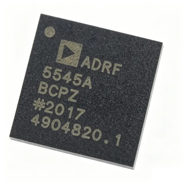
ADRF5545ABCPZN - Dual-Channel 2.4-4.2GHz RF Front End | Analog Devices
The ADRF5545ABCPZN is a dual-channel, integrated radio frequency (RF) front-end multichip module from Analog Devices, designed for time division duplexing (TDD) applications operating from 2.4 GHz to 4.2 GHz. It integrates low-noise amplifiers (LNAs) and power amplifiers (PAs) in a compact 40-lead LFCSP-VQ (6x6 mm) package, providing a complete RF front-end solution for wireless infrastructure and communication systems. An RF front end (LNA + PA) is a critical component in wireless transceivers that conditions the signal between the antenna and the baseband processor. It typically includes a low-noise amplifier (LNA) to boost weak received signals with minimal added noise, and a power amplifier (PA) to amplify transmitted signals to the required power level. The ADRF5545A integrates these functions in a dual-channel configuration, enabling MIMO and diversity schemes in TDD systems. Key features of the ADRF5545ABCPZN include dual-channel operation, wide frequency coverage from 2.4 GHz to 4.2 GHz, and integration of LNA and PA in a single module. The device is designed for TDD applications, where transmit and receive paths share the same frequency band but are time-multiplexed. The multichip module architecture ensures high isolation between channels and optimized performance for both receive and transmit paths. Technically, the ADRF5545A employs advanced RF design techniques to achieve low noise figure in the receive path and high linearity in the transmit path. The dual-channel configuration supports 2x2 MIMO systems, improving data throughput and link reliability. The module is housed in a 40-lead LFCSP-VQ package with an exposed pad for thermal management, ensuring reliable operation in high-power transmit scenarios. Typical applications include 5G NR TDD base stations, small cells, repeaters, and other wireless infrastructure equipment operating in the 2.4 GHz to 4.2 GHz band. The device is also suitable for point-to-point microwave links and radar systems that require compact, high-performance RF front ends. When designing with the ADRF5545ABCPZN, careful attention must be paid to PCB layout to minimize parasitic inductance and ensure proper grounding. The exposed pad should be soldered to a thermal via array to dissipate heat effectively. Additionally, the TDD switching control must be synchronized with the system timing to avoid signal leakage between transmit and receive paths.

ADRF5547BCPZN - Dual-Channel RF Front End 3.7-5.3GHz | Analog Devices
The ADRF5547BCPZN is a dual-channel, integrated RF front-end multichip module from Analog Devices, designed for time division duplexing (TDD) applications operating from 3.7 GHz to 5.3 GHz. It combines a cascading two-stage low noise amplifier (LNA) with a high-power silicon single-pole, double-throw (SPDT) switch in a compact 40-lead LFCSP-VQ (6x6 mm) package. This integration reduces board space and simplifies RF front-end design for 5G NR, massive MIMO, and other wireless infrastructure. An RF front end (RFFE) is the circuitry between the antenna and the digital baseband in a wireless transceiver. It typically includes low noise amplifiers (LNAs), power amplifiers (PAs), switches, filters, and matching networks. The ADRF5547 integrates the LNA and SPDT switch into a single module, reducing component count and improving performance by minimizing interconnect losses. This module is part of the broader RF front-end category, which is essential for signal conditioning in both transmit and receive paths. Key features include a noise figure of 1.6 dB, which ensures high receiver sensitivity, and a 40W SPDT switch capable of handling high transmit power. The dual-channel configuration supports diversity or MIMO applications, and the module operates over a wide supply voltage range. The LFCSP-VQ package offers excellent thermal performance and a small footprint, ideal for dense PCB layouts. Technically, the ADRF5547 uses a silicon SPDT switch with high linearity and power handling, while the two-stage LNA provides high gain and low noise. The module is designed for TDD systems where the same antenna is used for both transmit and receive, requiring fast switching between modes. The integrated design ensures minimal insertion loss and high isolation between channels. Typical applications include 5G NR base stations, small cells, massive MIMO arrays, and other TDD wireless infrastructure. The wide frequency range covers n77, n78, and n79 bands, making it versatile for global deployments. The module's high linearity and low noise make it suitable for both sub-6 GHz macro and small cell applications. When designing with the ADRF5547, ensure proper grounding and thermal management for the LFCSP-VQ package. The exposed pad should be soldered to a thermal via array to dissipate heat from the high-power switch. Also, consider the control logic timing for TDD switching to avoid signal degradation during transitions.