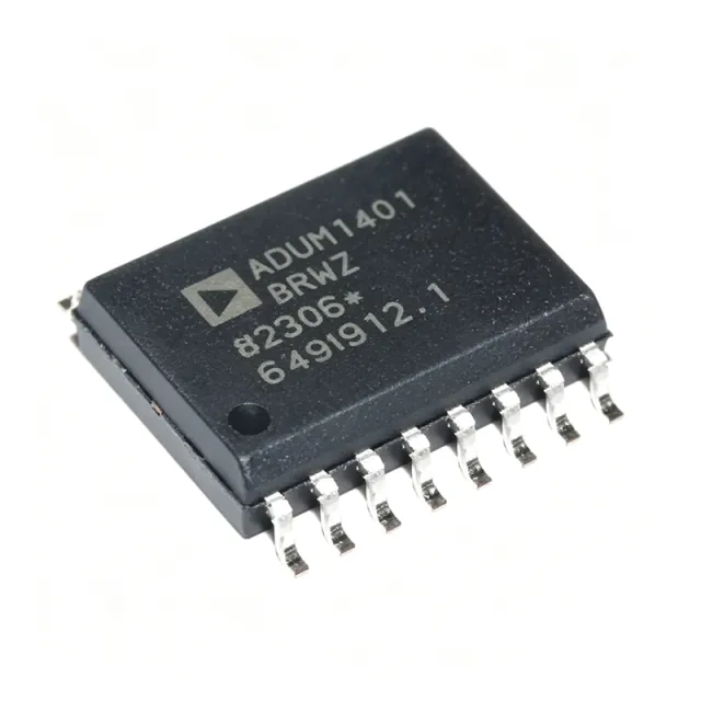
ADUM4221BRWZ - Isolated Half-Bridge Gate Driver | Analog Devices
N.º da peça: ADUM4221BRWZ ✓ Ativo| Qtd. | Preço unitário | Total |
|---|---|---|
| 1 | $4.85 | $4,85 |
| 10 | $4.36 | $43,60 |
| 100 | $3.88 | $388,00 |
| 500 | $3.49 | $1.745,00 |
| 1.000 | $3.1 | $3.100,00 |
ADUM4221BRWZ Visão geral
An isolated gate driver is a specialized IC that transfers switching signals across an isolation barrier while providing the high current needed to charge and discharge the gate capacitance of power transistors. It combines galvanic isolation (often via magnetic coupling) with level-shifting and drive circuitry, enabling safe and efficient control of high-voltage power stages from low-voltage control logic. In the hierarchy of power management, it sits between the controller (MCU/DSP) and the power switches, ensuring signal integrity and protecting low-voltage circuitry from high-voltage transients.
Key features of the ADUM4221BRWZ include 4 A peak output current, adjustable dead time via an external resistor, and a propagation delay of 60 ns (typical). The device supports a wide output supply range (VDDA/VDDB) from 4.5 V to 18 V, with UVLO thresholds of 7.5 V (typical) for both channels. It also features a disable pin for output shutdown and a CMOS input interface compatible with 2.5 V to 6.5 V logic. The isolation barrier is rated at 5 kVrms for 1 minute, with a working voltage of 560 Vrms, and the device is certified to UL 1577 and IEC 60747-5-5 (VDE 0884-10) standards.
Technically, the ADUM4221 uses iCoupler technology, which employs chip-scale transformers to transmit signals across the isolation barrier. This provides reliable operation with high common-mode transient immunity (CMTI) of 100 kV/us, ensuring stable performance in noisy power environments. The adjustable dead time feature allows designers to optimize switching behavior to prevent shoot-through in half-bridge topologies, improving efficiency and reliability.
Typical applications include isolated switch-mode power supplies, motor drives, solar inverters, and industrial automation. The device's high output current and fast switching speed make it ideal for driving large MOSFETs and IGBTs in high-power systems. Its wide input supply range and low propagation delay also suit high-frequency switching converters.
When designing with the ADUM4221BRWZ, ensure proper PCB layout to minimize parasitic inductance in the gate drive loop, and place the dead-time resistor close to the DT pin. Also, provide adequate decoupling on the output supplies to handle peak currents.
Alternativas drop-in para ADUM4221BRWZ — mesmo encapsulamento, compatível pino a pino. Peças de encapsulamento diferente que exigem retrabalho na PCB são excluídas.
Variantes desta série
Modelos da mesma série compatíveis como drop-in com ADUM4221BRWZ (mesmo formato e footprint) — diferindo em Adjustable Dead Time, Isolation Voltage, Package, Technology.
Ferramenta de comparação rápida — selecione peças alternativas para comparação lado a lado:
ADUM4221BRIZ
📋 Alternativa de referência (fora do catálogo)
ADUM4221BRIZ-RL
📋 Alternativa de referência (fora do catálogo)
ADUM4223BRWZ
📋 Alternativa de referência (fora do catálogo)
ADUM4221-1BRIZ
📋 Alternativa de referência (fora do catálogo)
ISO7721DW
✓ Em estoque
$1.45 / unidade
Ver ficha técnica →Si8233
📋 Alternativa de referência (fora do catálogo)
ADUM4221BRWZ Classificações máximas e características elétricas
| Technology | Magnetic Coupling (iCoupler) |
| Number of Channels | 2 |
| Peak Output Current | 4 A |
| Isolation Voltage | 5000 Vrms |
| Input Supply Voltage (VDD1) | 2.5 V to 6.5 V |
| Output Supply Voltage (VDDA/VDDB) | 4.5 V to 18 V |
| UVLO Threshold | 7.5 V (typical) |
| Propagation Delay | 60 ns (typical) |
| Common-Mode Transient Immunity (CMTI) | 100 kV/us |
| Adjustable Dead Time | Yes (via external resistor) |
| Encapsulamento | 16-SOIC (wide body) |
| Faixa de temperatura de operação | -40°C to +125°C |
| Status RoHS | Compliant |
| Nível MSL | 3 (168 hours) |
| Tipo de montagem | Surface Mount |
Configuração de pinos do ADUM4221BRWZ
| Pino 1 | VDD1 — Input supply voltage (2.5 V to 6.5 V) |
| Pino 2 | GND1 — Input ground |
| Pino 3 | VIA — Input A (non-inverting) |
| Pino 4 | VIB — Input B (non-inverting) |
| Pino 5 | DISABLE — Disable input (active high) |
| Pino 6 | DT — Dead time adjust |
| Pino 7 | GND1 — Input ground |
| Pino 8 | NC — No connect |
| Pino 9 | VDDA — Output supply A (4.5 V to 18 V) |
| Pino 10 | VOA — Output A |
| Pino 11 | GNDA — Output ground A |
| Pino 12 | GNDB — Output ground B |
| Pino 13 | VOB — Output B |
| Pino 14 | VDDB — Output supply B (4.5 V to 18 V) |
| Pino 15 | NC — No connect |
| Pino 16 | GND1 — Input ground |
Aplicações típicas
ADUM4221BRWZ é adequado para 6 aplicaçãos: Isolated Switch-Mode Power Supplies, Motor Drives, Solar Inverters, Industrial Automation, Electric Vehicle Chargers, Renewable Energy Systems.
Isolated Switch-Mode Power Supplies
The ADUM4221BRWZ is ideal for isolated DC-DC converters and switch-mode power supplies where high-side and low-side MOSFETs need to be driven with galvanic isolation. Its 4 A peak output current ensures fast switching of large gate capacitances, while the 5 kVrms isolation protects low-voltage control circuitry from high-voltage transients. The adjustable dead time prevents shoot-through, improving efficiency and reliability. With a propagation delay of 60 ns, it supports high-frequency operation up to several hundred kHz, making it suitable for compact power supplies.
Recomendado
Motor Drives
In motor drive applications, the ADUM4221BRWZ provides isolated gate drive for the high-side and low-side switches in a half-bridge or full-bridge inverter. Its high CMTI of 100 kV/us ensures reliable operation in noisy environments with fast voltage transients. The adjustable dead time allows optimization of switching to minimize losses and prevent shoot-through. The wide output supply range (4.5 V to 18 V) accommodates various gate drive voltages for IGBTs and MOSFETs. This makes it suitable for industrial motor control, robotics, and automotive traction inverters.
Recomendado
Solar Inverters
The ADUM4221BRWZ is well-suited for solar inverter applications, where it drives the power switches in the DC-AC conversion stage. Its 5 kVrms isolation provides the necessary galvanic isolation between the high-voltage DC bus and the control electronics. The 4 A peak output current enables efficient switching of large IGBTs, while the adjustable dead time helps optimize efficiency and reduce EMI. The device's wide operating temperature range (-40°C to +125°C) ensures reliable operation in outdoor environments. Its high CMTI also ensures stable performance under fast voltage transients common in solar inverters.
Recomendado
Industrial Automation
In industrial automation, the ADUM4221BRWZ is used in isolated gate drive circuits for motor controls, robotics, and power supplies. Its robust isolation (5 kVrms) and high CMTI (100 kV/us) ensure reliable operation in harsh industrial environments with high electrical noise. The adjustable dead time feature allows precise control of switching to prevent shoot-through and reduce EMI. The device's wide input supply range (2.5 V to 6.5 V) makes it compatible with various logic levels, simplifying integration with microcontrollers and PLCs. Its 16-SOIC package is compact and suitable for space-constrained industrial PCBs.
Recomendado
Electric Vehicle Chargers
The ADUM4221BRWZ is suitable for electric vehicle (EV) chargers, where it drives the power switches in the AC-DC and DC-DC conversion stages. Its 5 kVrms isolation provides the required galvanic isolation between the high-voltage battery and the control electronics. The 4 A peak output current ensures efficient switching of high-power IGBTs and MOSFETs, while the adjustable dead time helps optimize efficiency and reduce EMI. The device's wide operating temperature range and high CMTI make it reliable in automotive environments. Its compact 16-SOIC package is ideal for space-constrained charger designs.
Recomendado
Renewable Energy Systems
The ADUM4221BRWZ is used in renewable energy systems such as wind turbines and energy storage systems, where it drives power switches in inverters and converters. Its high isolation voltage (5 kVrms) and CMTI (100 kV/us) ensure reliable operation in high-voltage, noisy environments. The adjustable dead time allows optimization of switching to maximize efficiency and minimize losses. The device's wide input supply range (2.5 V to 6.5 V) makes it compatible with various control logic, and its 16-SOIC package is suitable for compact power electronics. This makes it a versatile choice for renewable energy applications.
Recomendado
Resumo dos produtos recomendados
Dados de referência de engenharia para ADUM4221BRWZ — comparação, orientação de projeto e informações de conformidade.
Guia de seleção
Comparação com alternativas
| Parâmetro | Este produto | ADUM4221BRIZ | ADUM4223BRWZ | ISO7721 |
|---|---|---|---|---|
| Package | 16-SOIC | 16-SOIC | 16-SOIC | 16-SOIC |
| Brand | Analog Devices | Analog Devices | Analog Devices | Texas Instruments |
| Peak Output Current | 4 A | 4 A | 4 A | 4 A |
| Isolation Voltage | 5000 Vrms | 5000 Vrms | 5000 Vrms | 5000 Vrms |
| Adjustable Dead Time | Yes | Yes | No | No |
| Input Configuration | Dual Input (VIA, VIB) | Dual Input | Single Input with Enable | Dual Input |
| Propagation Delay | 60 ns | 60 ns | 60 ns | 16 ns |
| CMTI | 100 kV/us | 100 kV/us | 100 kV/us | 100 kV/us |
Principais diferenciais
- Adjustable dead time (vs ADUM4223BRWZ)
- Dual independent inputs (vs ADUM4223BRWZ)
- Higher CMTI (vs ISO7721)
Notas de projeto
For optimal performance, place the ADUM4221BRWZ close to the power switches to minimize gate drive loop inductance. Use wide, short traces for the gate drive outputs (VOA, VOB) and ensure a solid ground plane for GNDA and GNDB. Add a 0.1 uF ceramic capacitor close to each output supply pin (VDDA, VDDB) and a 1 uF bulk capacitor for peak current demands.
The ADUM4221BRWZ dissipates power primarily during switching. At 4 A peak output and high switching frequencies, ensure adequate thermal relief. The 16-SOIC package has a thermal resistance of approximately 80°C/W (theta_JA). For high-power applications, provide a copper pour under the device and consider a thermal pad if available. Monitor junction temperature to stay below 125°C.
Do not exceed the absolute maximum ratings: VDD1 up to 7 V, VDDA/VDDB up to 20 V. Ensure the dead time resistor is connected to the DT pin to set the desired dead time; leaving it floating may cause unpredictable behavior. Also, avoid driving the DISABLE pin with voltages above VDD1. Use proper bypassing on VDD1 to prevent noise coupling.
Informações de conformidade
RoHS compliant per Analog Devices product page. Not AEC-Q100 qualified. Lead-free finish.






