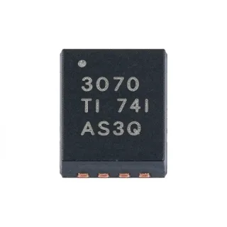
CD4060BK - 14-Stage CMOS Counter/Divider | Texas Instruments
N.º da peça: CD4060BK ✓ AtivoCD4060BK Visão geral
A binary counter is a digital sequential circuit that stores and advances a count using binary-weighted stages. A divider extends this function by dividing an input frequency into a lower output frequency. The CD4000 CMOS logic family belongs to the broader logic IC and counter/divider hierarchy, combining low-power operation with wide supply-voltage flexibility. The oscillator and counter functions are commonly used together in timers, clock dividers, and programmable pulse-generation circuits.
The verified CD4060B family data identifies 14 ripple-carry stages, operation from 3 V to 18 V, and a maximum clock frequency of 24 MHz. These ratings support both low-voltage logic systems and higher-voltage industrial or instrumentation environments. Its 16-CFP package offers a surface-mount option for compact assemblies, while the broad -55°C to +125°C temperature range supports demanding operating conditions.
The ripple-carry architecture means each counting stage advances after the preceding stage, with the counter incrementing on the negative transition of the clock. Designers should account for accumulated propagation delay when dividing high frequencies or interpreting the relationship between clock edges and output transitions. The operating-frequency limit and external oscillator-component requirements must be checked against the manufacturer datasheet before establishing timing margins in a new circuit.
Typical uses include divide-by-16 through divide-by-16384 clock generation, retriggerable pulse timing, periodic-event generation, and low-frequency clock derivation from a higher-frequency source. The oscillator pins can support an external resistor-capacitor network when stable autonomous operation is required, while an external clock can be applied when the system already provides a timing reference.
PCB implementation should preserve short oscillator and clock paths, provide an unobstructed ground reference, and decouple the supply close to the device. Because the CFP-16 footprint is temperature- and package-sensitive, assembly should follow the manufacturer’s soldering and land-pattern recommendations. The verified source does not provide a complete pin-level table, so the final design should use the official CD4060B datasheet rather than an inferred pinout.
This page consolidates verified manufacturer and distributor information, exact CD4060BK pricing evidence, package and environmental ratings, application guidance, and data-gap disclosures. It distinguishes documented facts from unavailable parameters and avoids presenting unverified substitute parts as drop-in replacements.
Alternativas drop-in para CD4060BK — mesmo encapsulamento, compatível pino a pino. Peças de encapsulamento diferente que exigem retrabalho na PCB são excluídas.
Nenhuma alternativa drop-in disponível para este produto.
Solicitar alternativasCD4060BK Classificações máximas e características elétricas
| Product Type | CMOS 14-stage ripple-carry binary counter/divider and oscillator |
| Logic Family | CD4000 CMOS series |
| Number of Counter Stages | 14 stages |
| Counter Output Width | 14 bit |
| Number of Counter Elements | 1 element |
| Supply Voltage Range | 3 V to 18 V |
| Frequência máxima de clock | 24 MHz |
| Clock Edge | Falling edge |
| Counting Transition | Negative transition of each clock pulse |
| Faixa de temperatura de operação | -55°C to +125°C |
| Encapsulamento | 16-CFP flat-pack surface-mount package |
| Tipo de montagem | Surface mount |
| Tipo de saída | Binary counter output |
| Oscillator | Integrated |
| Quiescent Current Test Condition | 100% tested at 20 V |
| Parametric Rating Voltages | 5 V, 10 V, and 15 V |
Guia de Configuração de Pinos do CD4060BK 16-cfp flat-pack surface-mount package
Configuração de pinos para CD4060BK (pacote 16-cfp flat-pack surface-mount package). Este CI digital inclui GPIO, interfaces de comunicação (UART, SPI, I2C) e pinos de alimentação. Consulte o datasheet do fabricante para funções alternativas dos pinos e opções de configuração. Essencial para projeto de sistemas embarcados e layout de PCB.

Nenhum dado detalhado de pinagem disponível para CD4060BK.
Consulte a ficha técnica para a configuração completa dos pinos.
Aplicações típicas
CD4060BK é adequado para 6 aplicaçãos: Programmable Clock Divider, Retriggerable Pulse Timer, Periodic Event Generator, Industrial Control Sequencing, Low-Frequency Instrumentation Clock, Watchdog and Retiming Circuit.
Programmable Clock Divider
The CD4060BK fits clock-divider designs because its 14 ripple-carry stages provide successive divide ratios through the binary outputs, while the documented 24 MHz maximum clock frequency supports conventional digital timing systems. A system clock can be applied to the clock input and the required divide-by-2 through divide-by-16384 output selected. Because the architecture is ripple-carry, accumulated propagation delay must remain compatible with the receiving circuit’s setup and hold requirements. The 3 V to 18 V supply range also allows the divider to share power with both low-voltage and higher-voltage CMOS systems.
Recomendado
Retriggerable Pulse Timer
The CD4060BK can support retriggerable pulse-timing and monostable-style arrangements by combining its oscillator with 14 counter outputs. Designers can determine the desired timing interval from the selected stage and then use the output edge to trigger or reset downstream circuitry. The integrated oscillator reduces the number of separate timing components required when an autonomous time base is acceptable. Its -55°C to +125°C operating range is useful in demanding industrial timing circuits, although oscillator accuracy and temperature stability must be verified from the official manufacturer data before treating it as a precision time reference.
Recomendado
Periodic Event Generator
A CD4060BK is appropriate for periodic-event generation because the binary counter outputs provide predictable division points derived from the oscillator or external clock. A selected output can periodically enable a relay, update a display, sample another circuit, or initiate a communication sequence. The documented 24 MHz clock capability gives designers substantial timing headroom compared with slower signal frequencies, while the 3 V to 18 V range permits operation across multiple logic-rail environments. In a new design, confirm output rise and fall times, propagation delays, and reset behavior in the CD4060B datasheet.
Recomendado
Industrial Control Sequencing
CD4060BK can divide a system time base into slower control intervals used to sequence relays, actuators, counters, or subsystem enables. Its 14-stage counter structure allows several timing divisions from one oscillator, helping avoid independent timer blocks when coarse timing is sufficient. The wide 3 V to 18 V supply range and -55°C to +125°C temperature rating support many industrial environments, while the 16-CFP package is suitable for automated surface-mount assembly. Reset synchronization and isolation must be added where multiple timers must restart coherently or where a fault could cause an unsafe output sequence.
Recomendado
Low-Frequency Instrumentation Clock
The CD4060BK can derive a low-frequency service clock from a higher-frequency source in test and measurement equipment. Divide the input through the available binary stages, condition the selected output, and distribute it to sampling or status circuits. The documented 3 V to 18 V supply range allows operation near the voltage used by many legacy CMOS control systems, and the 24 MHz maximum clock frequency is suitable for common timing architectures. For accurate measurement results, however, the engineer must distinguish a functional divider from a precision frequency reference and account for oscillator drift and ripple propagation delay.
Recomendado
Watchdog and Retiming Circuit
CD4060BK can implement timeout or watchdog-style functions by counting oscillator or system-clock pulses and generating an event when a selected stage overflows or reaches its expected state. The resulting signal can request a reset, inhibit an actuator, or alert a controller. Its 14 counting stages permit multiple timeout ranges without a separate timer for each interval, and the 16-CFP package supports compact PCB layouts. Because a ripple counter’s timing depends on propagation through multiple stages, reset release behavior and fault-response latency should be checked carefully in the official datasheet, especially for safety-related equipment.
Recomendado
Resumo dos produtos recomendados
Dados de referência de engenharia para CD4060BK — comparação, orientação de projeto e informações de conformidade.
Guia de seleção
Notas de projeto
Keep the oscillator network and clock-input traces short, and route them away from high-current switching nodes. The verified records do not include the exact pin map or recommended layout artwork, so the official Texas Instruments CD4060B datasheet should control placement. Place the device near its decoupling capacitor and provide a continuous ground path to reduce switching-induced timing errors.
Do not assume that every CD4060B suffix is a mechanical drop-in for CD4060BK. The target is documented in a 16-CFP surface-mount package, while other family members may use different package constructions. Verify pin names, pin numbering, land dimensions, and exposed thermal features on the replacement datasheet before approving any substitution; the supplied cross-reference results did not establish a qualified drop-in replacement.
Account for cumulative ripple-carry propagation delay when using a high-stage output at a high input frequency. Although the device is documented up to 24 MHz, the usable timing margin also depends on the selected output stage and the receiving circuit. Add reset synchronization and test the clock, reset, and decoded outputs together because asynchronous release or ringing can create false count events in a timing system.
Informações de conformidade
The verified Texas Instruments datasheet snippet states that the CD4060B family meets the requirements of JEDEC Tentative Standard No. 13B for B-series CMOS devices. No verified RoHS, REACH, AEC-Q100, lead-free, halogen-free, or conflict-minerals declaration was supplied.