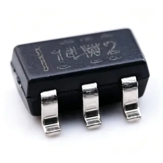
INA293B1QDBVRQ1 - 110V, 1.3MHz Current Sense Amp | TI
N.º da peça: INA293B1QDBVRQ1 ✓ Ativo| Qtd. | Preço unitário | Total |
|---|---|---|
| 1 | $1.95 | $1,95 |
| 10 | $1.72 | $17,20 |
| 100 | $1.34 | $134,00 |
| 500 | $1.06 | $530,00 |
| 1.000 | $0.88 | $880,00 |
INA293B1QDBVRQ1 Visão geral
What is a current-sense amplifier? A current-sense amplifier is a specialized analog building block that measures the small differential voltage developed across a shunt resistor placed in series with a load or supply rail, and converts it to a ground-referenced output voltage proportional to load current. Unlike a general-purpose op amp, a current-sense amplifier tolerates large common-mode voltages - often well above its own supply - and rejects the common-mode component, exposing only the shunt drop. The INA293-Q1 sits at the high-precision end of this category, combining low offset, low drift, and the widest common-mode range in TI's portfolio of unidirectional/bidirectional current-sense amplifiers.
Key features include a maximum offset voltage of ±30 µV across temperature, ±0.2% gain error, and a quiescent current of approximately 1.5 mA over the -40 °C to +125 °C automotive grade-1 temperature range. The B1 gain variant provides 20 V/V; the B2, B3, B4, and B5 variants in the same family offer 50 V/V, 100 V/V, 200 V/V, and 500 V/V respectively, all sharing the SOT-23-5 footprint. The device operates from a single 2.7 V to 20 V supply and is robust against input transients well beyond its supply rail.
Internally, the INA293-Q1 uses a precision chopped-input front end followed by a fixed-gain output stage, achieving CMRR greater than 100 dB at DC and PSRR above 80 dB at 1 kHz. The wide common-mode architecture supports both high-side and low-side sensing topologies, enabling accurate monitoring in 48 V mild-hybrid automotive systems, industrial 24 V/36 V/48 V rails, and telecom -48 V applications without level shifting.
Typical applications include 48 V eMobility battery management, BLDC motor phase-current monitoring, server/AI accelerator hot-swap current telemetry, USB Power Delivery contract current sensing, and solar inverter string monitoring. Compared with isolated current transducers, the INA293-Q1 achieves comparable accuracy at a fraction of the BOM cost and PCB area.
When designing with this device, place the shunt resistor as close as possible to the input pins and keep the input traces symmetrical to preserve CMRR. A 0.1 µF supply bypass capacitor placed within 5 mm of the V+ pin is recommended for stable operation across the full -4 V to +110 V common-mode range.
This page synthesizes distributor pricing, drop-in alternatives from the INA293-Q1 family and competing high-side current-sense amplifiers, and practical design notes that go beyond the manufacturer datasheet.
Alternativas drop-in para INA293B1QDBVRQ1 — mesmo encapsulamento, compatível pino a pino. Peças de encapsulamento diferente que exigem retrabalho na PCB são excluídas.
Ferramenta de comparação rápida — selecione peças alternativas para comparação lado a lado:
INA293B2QDBVRQ1
✅ Drop-In📋 Alternativa de referência (fora do catálogo)
INA293B3QDBVRQ1
✅ Drop-In📋 Alternativa de referência (fora do catálogo)
INA293B4QDBVRQ1
✅ Drop-In📋 Alternativa de referência (fora do catálogo)
INA293B5QDBVRQ1
✅ Drop-In📋 Alternativa de referência (fora do catálogo)
INA293B1DBVR
✅ Drop-In📋 Alternativa de referência (fora do catálogo)
INA240A2QDRQ1
✅ Drop-In📋 Alternativa de referência (fora do catálogo)
INA293B1QDBVRQ1 Classificações máximas e características elétricas
| Product Type | Bidirectional Current-Sense Amplifier |
| Common-Mode Input Range | -4 V to +110 V |
| Supply Voltage Range | 2.7 V to 20 V |
| Small-Signal Bandwidth | 1.3 MHz |
| Fixed Gain (B1 variant) | 20 V/V |
| Gain Error (max) | ±0.2% |
| CMRR at DC | >100 dB |
| PSRR at 1 kHz | >80 dB |
| Faixa de temperatura de operação | -40 °C to +125 °C (AEC-Q100 Grade 1) |
| Encapsulamento | SOT-23-5 (DBV) |
| Tipo de montagem | Surface Mount |
| Nível MSL | 1 (per TI datasheet) |
| Automotive Qualification | AEC-Q100 Qualified (Grade 1) |
| Status RoHS | Compliant |
| Lead Finish | NiPdAu (Lead-free) |
| Canais | 1 |
| Gain Variant Code | B1 (20 V/V); family also includes B2/B3/B4/B5 |
Configuração de pinos do INA293B1QDBVRQ1
| Pino 1 | IN+ — Positive (high-side) differential input; connects to load-side of shunt |
| Pino 2 | GND — Device ground; connect to system ground |
| Pino 3 | IN- — Negative (low-side) differential input; connects to GND-side of shunt |
| Pino 4 | OUT — Output voltage; VOUT = (V_IN+ − V_IN-) × GAIN |
| Pino 5 | V+ — Supply voltage; 2.7 V to 20 V, decouple with 0.1 µF to GND |
Aplicações típicas
INA293B1QDBVRQ1 é adequado para 6 aplicaçãos: 48 V Mild-Hybrid Automotive BMS, BLDC Motor Phase-Current Monitoring, AI Server Hot-Swap Current Telemetry, USB Power Delivery Contract-Current Sensing, Solar String Current Monitoring, Industrial 24 V / 48 V Solenoid & Actuator Monitoring.
48 V Mild-Hybrid Automotive BMS
The INA293B1QDBVRQ1 is a near-ideal choice for high-side current monitoring in 48 V mild-hybrid (MHEV) battery management systems. Its -4 V to +110 V common-mode range directly accommodates the nominal 48 V rail plus transient excursions up to ~52 V and reverse-polarity events, eliminating the need for external level shifters. The 20 V/V gain of the B1 variant is well-matched to a 1 mΩ shunt at 100 A loads, producing a 2 V full-scale output that fits comfortably within the 2.7 V to 20 V supply headroom. AEC-Q100 Grade-1 qualification (-40 °C to +125 °C) and ±0.2% gain error over temperature make this part suitable for ASIL-B capable BMS designs when paired with a redundant channel. Reference: TI INA293-Q1 datasheet, 'Typical Applications' section.
Recomendado
BLDC Motor Phase-Current Monitoring
Phase-current feedback in brushless DC motor drives demands accurate sensing across a wide common-mode range because the phase voltage swings from ground to the DC bus voltage at every PWM edge. The INA293B1QDBVRQ1's -4 V to +110 V common-mode tolerance allows its shunt to be placed directly in the phase leg without protection, simplifying the inverter layout. With 1.3 MHz small-signal bandwidth the amplifier tracks PWM edges cleanly and supports field-oriented control (FOC) at switching frequencies up to ~100 kHz. The 20 V/V fixed gain (B1) suits a 2 mΩ shunt at 30 A peak phase current, producing a 1.2 V full-scale signal well inside the ADC input range of companion C2000 MCUs. AEC-Q100 Grade-1 qualification supports automotive motor-control designs.
Recomendado
AI Server Hot-Swap Current Telemetry
AI accelerator cards and GPU modules in hyperscale servers draw 600 W to 1200 W from 48 V distribution buses; the hot-swap controller must accurately sense inrush and steady-state load currents to detect faults. The INA293B1QDBVRQ1's -4 V to +110 V common-mode range suits the 48 V bus directly, while 1.3 MHz bandwidth enables fast overcurrent response at sub-microsecond latencies. With a 0.5 mΩ shunt the B1 (20 V/V) variant produces 10 mV/A, sufficient resolution to detect 1 A load steps in a 600 A system. The SOT-23-5 footprint is small enough to fit adjacent to board-edge connectors, preserving routing density in dense AI server backplanes. Reference: TI INA293-Q1 datasheet, 'Application Information' section.
Recomendado
USB Power Delivery Contract-Current Sensing
USB Power Delivery 3.1 Extended Power Range (EPR) supports 28 V, 36 V, and 48 V fixed and programmable supply modes, with current up to 5 A (240 W EPR). The INA293B1QDBVRQ1 measures the VBUS current on the source side while withstanding the full VBUS voltage up to 110 V during transient events. With the B1 (20 V/V) gain and a 10 mΩ sense resistor, the part delivers 200 mV/A, yielding a 1 V full-scale signal at 5 A - well within the ADC range of the PD controller. The wide CMRR (>100 dB at DC) ensures that ripple from the buck-boost converter does not corrupt current telemetry used for thermal foldback and cable-compensation algorithms. Reference: TI INA293-Q1 datasheet, USB-PD reference design.
Recomendado
Solar String Current Monitoring
Solar inverters must monitor the DC string current to detect arc faults, module degradation, and bypass-diode failures. The INA293B1QDBVRQ1's -4 V to +110 V common-mode range accommodates open-circuit string voltages up to 110 V (typical residential 1500 V system strings are built from series-connected 110 V-class module groups), and its 1.3 MHz bandwidth captures fast arc signatures. With a 5 mΩ shunt the B1 variant produces 100 mV/A, providing 1 A resolution at the typical 15-20 A string current. The AEC-Q100 Grade-1 qualification - while primarily automotive - indicates robustness that benefits harsh outdoor solar environments with wide temperature swings. Reference: TI INA293-Q1 datasheet, 'Solar Inverter' typical application.
Recomendado
Industrial 24 V / 48 V Solenoid & Actuator Monitoring
Factory automation actuators and proportional solenoids operate from 24 V and 48 V industrial rails with high inrush currents that must be measured for closed-loop control and health diagnostics. The INA293B1QDBVRQ1 monitors current on the high side while tolerating inductive flyback transients up to 110 V, eliminating the need for external TVS clamps in many designs. The 1.3 MHz bandwidth supports PWM-driven proportional valves at carrier frequencies up to several kHz without aliasing. The B1 (20 V/V) gain with a 10 mΩ shunt produces 200 mV/A - adequate for diagnostics on 1-10 A solenoids. The SOT-23-5 footprint fits inside the actuator housing or on compact PLC daughter boards.
Recomendado
Resumo dos produtos recomendados
Dados de referência de engenharia para INA293B1QDBVRQ1 — comparação, orientação de projeto e informações de conformidade.
Guia de seleção
Comparação com alternativas
| Parâmetro | Este produto | INA293B2QDBVRQ1 | INA293B3QDBVRQ1 | INA293B4QDBVRQ1 | INA293B5QDBVRQ1 | INA293B1DBVR |
|---|---|---|---|---|---|---|
| Brand | Texas Instruments | Texas Instruments | Texas Instruments | Texas Instruments | Texas Instruments | Texas Instruments |
| Package | SOT-23-5 (DBV) | SOT-23-5 (DBV) - same | SOT-23-5 (DBV) - same | SOT-23-5 (DBV) - same | SOT-23-5 (DBV) - same | SOT-23-5 (DBV) - same |
| Fixed Gain | 20 V/V (B1) | 50 V/V (B2) | 100 V/V (B3) | 200 V/V (B4) | 500 V/V (B5) | 20 V/V (B1) |
| Common-Mode Range | -4 V to +110 V | -4 V to +110 V (same) | -4 V to +110 V (same) | -4 V to +110 V (same) | -4 V to +110 V (same) | -4 V to +110 V (same) |
| Bandwidth | 1.3 MHz | 1.3 MHz | 1.3 MHz | 1.3 MHz | 1.3 MHz | 1.3 MHz |
| Supply Range | 2.7 V to 20 V | 2.7 V to 20 V | 2.7 V to 20 V | 2.7 V to 20 V | 2.7 V to 20 V | 2.7 V to 20 V |
| AEC-Q100 Qualification | Grade 1 (Yes) | Grade 1 (Yes) | Grade 1 (Yes) | Grade 1 (Yes) | Grade 1 (Yes) | No (industrial only) |
| Operating Temperature | -40 °C to +125 °C | -40 °C to +125 °C | -40 °C to +125 °C | -40 °C to +125 °C | -40 °C to +125 °C | -40 °C to +125 °C |
Principais diferenciais
- Widest common-mode range in TI current-sense portfolio (vs INA240A-Q1)
- Five pin-compatible gain variants in one family (vs INA181 (single-gain family))
- 1.3 MHz bandwidth for PWM-edge-aware motor control (vs INA181 (350 kHz max))
Notas de projeto
Route the IN+ and IN- traces as a symmetric differential pair directly from the shunt resistor to the device pins. Keep trace length below 5 mm and avoid vias in the input path; the Kelvin connection to the shunt is critical for preserving the datasheet's ±0.2% gain error. Place a 0.1 µF X7R bypass capacitor within 5 mm of the V+ pin and a 10 µF bulk capacitor nearby to suppress supply ripple from upstream DC-DC converters.
Do not place any resistance between the shunt and the IN+/IN- pins - even 10 mΩ of PCB trace resistance plus 1 mΩ of shunt produces a 10% gain error that will swamp the part's ±0.2% accuracy. The SOT-23-5 footprint has no exposed thermal pad, so power dissipation is limited to the package rating; for continuous high-side sensing above 50 V common-mode, verify that total power (V+ × IQ + VCM × leakage) stays within the 200 mW absolute maximum.
The 1.3 MHz small-signal bandwidth makes the INA293B1QDBVRQ1 sensitive to capacitive loading on the OUT pin; keep load capacitance below 100 pF to avoid peaking or instability. If driving an ADC input (which often presents tens of pF), add a 100 Ω series resistor between OUT and the ADC pin to isolate the capacitance. For long output traces (>50 mm), use a buffer amplifier or shielded cable to prevent EMI pickup from PWM edges in motor-control applications.
Informações de conformidade
AEC-Q100 Grade 1 qualified per TI INA293-Q1 datasheet. RoHS and REACH compliant. Lead-free NiPdAu finish. Halogen-free per TI's standard qualification matrix.