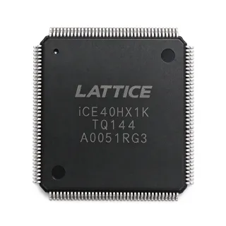
LFE2-6SE-5T144I - 6K LUT FPGA, 90 I/O, TQFP-144 | Lattice
N.º da peça: LFE2-6SE-5T144I ✓ AtivoLFE2-6SE-5T144I Visão geral
An FPGA is a semiconductor device whose digital logic is configured after manufacture. By combining programmable lookup-table logic, programmable interconnect, memory resources, and dedicated input/output blocks, an FPGA allows one physical device to implement functions that might otherwise require several discrete logic devices. Within the broader semiconductor hierarchy, an FPGA belongs to the programmable-logic family, alongside CPLDs, and provides higher implementation flexibility than fixed-function logic.
The LFE2-6SE-5T144I provides 6,000 FPGA logic cells and 6K LUTs, giving a design engine approximately 12,000 registers when both halves of each logic cell are used. Its 90 I/O pins support connections to external memories, processors, sensors, communications transceivers, and industrial peripherals. The 1.2 V core supply identifies it as a modern low-voltage FPGA architecture, while the -5 grade denotes its speed position within the ECP2 ordering system. The part is intended for industrial environments rather than the extended automotive grade.
The ECP2 implementation includes DSP-oriented resources suited to arithmetic and filtering functions, as well as serial-interface capabilities referenced in the product description. These resources allow designers to consolidate signal-processing and control logic into a single programmable device. The 144-pin TQFP package also exposes substantially more device connectivity than smaller FPGA packages, making the device appropriate for designs that need multiple parallel buses, memory interfaces, or external control signals.
Typical uses include industrial automation controllers, data-acquisition systems, communications equipment, embedded processing adjuncts, and general-purpose embedded control. In a data-acquisition system, its parallel I/O can connect to converters or sensors while programmable logic performs filtering, protocol handling, and control. In industrial equipment, the -5 speed grade and industrial temperature designation align with long-running control systems where device availability and deterministic logic performance are important.
Designers should match the selected ECP2 pinout, bank voltage requirements, configuration method, memory interface, and differential I/O constraints against the exact 144-pin device documentation. Power planning should include separate treatment of the 1.2 V core and applicable I/O supply rails. Configuration signals, clocking, decoupling, and serial programming connections must also be verified against the manufacturer pin-description and configuration guidance before schematic release.
This product page combines the core ECP2 device facts with package-aware replacement guidance, design considerations, and application-focused engineering context. It helps distinguish speed, temperature, and package suffix changes that otherwise look interchangeable but can affect qualification, timing, and production sourcing decisions.
Alternativas drop-in para LFE2-6SE-5T144I — mesmo encapsulamento, compatível pino a pino. Peças de encapsulamento diferente que exigem retrabalho na PCB são excluídas.
Variantes desta série
Modelos da mesma série compatíveis como drop-in com LFE2-6SE-5T144I (mesmo formato e footprint) — diferindo em Device Type, Package, Core Supply Voltage, DSP Capability, Logic Technology.
LFE2-6SE-5TN144I
✅ Drop-In📋 Alternativa de referência (fora do catálogo)
LFE2-6SE-5TN144C
✅ Drop-In📋 Alternativa de referência (fora do catálogo)
LFE2-6E-5T144I
✅ Drop-InConsulte o preço
Ver ficha técnica →LFE2-6SE-6TN144I
✅ Drop-In📋 Alternativa de referência (fora do catálogo)
LFE2-6E-5TN144C
✅ Drop-InConsulte o preço
Ver ficha técnica →LFE2-6SE-5T144I Classificações máximas e características elétricas
| Device Type | ECP2 Field Programmable Gate Array (FPGA) IC |
| FPGA Logic Cells | 6,000 cells |
| Look-Up Tables | 6K LUTs |
| User I/O | 90 I/O |
| Core Supply Voltage | 1.2 V |
| Speed Grade | -5 |
| Temperature Grade | Industrial |
| Encapsulamento | 144-pin TQFP |
| Package Body Size | 20 mm x 20 mm |
| Estilo de montagem | Surface Mount |
| DSP Capability | Yes |
| Serial Capability | S-Series DSP and S-Ser |
| Logic Technology | 90 nm |
| Lead-Free Status | Lead Free |
Guia de Configuração de Pinos do LFE2-6SE-5T144I 20 mm x 20 mm
Configuração de pinos para LFE2-6SE-5T144I (pacote 20 mm x 20 mm). Este CI digital inclui GPIO, interfaces de comunicação (UART, SPI, I2C) e pinos de alimentação. Consulte o datasheet do fabricante para funções alternativas dos pinos e opções de configuração. Essencial para projeto de sistemas embarcados e layout de PCB.

Nenhum dado detalhado de pinagem disponível para LFE2-6SE-5T144I.
Consulte a ficha técnica para a configuração completa dos pinos.
Aplicações típicas
LFE2-6SE-5T144I é adequado para 6 aplicaçãos: Industrial Automation Controller, Data-Acquisition System, Communications Interface Controller, Embedded Signal Processing, Programmable Logic Consolidation, Video and Display Control.
Industrial Automation Controller
The LFE2-6SE-5T144I fits an industrial automation controller because its 6K LUTs can implement sequencing, state machines, and protocol logic while 90 I/O connect sensors, actuators, and field-bus transceivers. The 1.2 V core supply simplifies modern digital power architecture, and the industrial-grade ordering option supports equipment designed for extended industrial environments. Engineers should reserve I/O pins for configuration, clocking, and status indicators, then verify bank voltage requirements against each connected interface. Timing closure must include the external transceiver and sensor delays rather than relying on FPGA logic timing alone.
Recomendado
Data-Acquisition System
The LFE2-6SE-5T144I can consolidate acquisition control around parallel converters, sensors, and digital interfaces. Its 6K LUT capacity is suitable for digital filtering, sample control, calibration sequencing, and interface conversion, while 90 I/O provide ample connectivity for converter data buses, triggers, and status signals. Use a dedicated clock-capable input for timing-critical paths and keep analog conversion hardware outside the FPGA. The 1.2 V core rail must be isolated cleanly from switching converter and I/O supplies to prevent noise from affecting acquisition accuracy.
Recomendado
Communications Interface Controller
The LFE2-6SE-5T144I is appropriate for communications equipment that needs programmable framing, buffering, packet handling, and parallel control around S-Series interface resources. Its 6K LUTs support moderate-complexity protocol logic, and the 90 I/O can connect transceivers, memories, and host processors. Designers should use the manufacturer interface documentation to confirm supported differential I/O arrangements, voltage levels, and clocking constraints. Keep high-speed serial traces away from sensitive configuration paths and provide continuous power and ground distribution that matches the selected I/O bank requirements.
Recomendado
Embedded Signal Processing
The LFE2-6SE-5T144I can serve as a compact signal-processing engine for digital filters, correlation, waveform generation, and control functions. Its ECP2 DSP resources complement the 6K LUT fabric, allowing arithmetic pipelines and supervisory logic to coexist in one device. The 90-I/O count provides access to converters, memory, and synchronized peripherals without requiring multiple programmable devices. Resource sharing should be planned carefully: arithmetic pipelines, register stages, and block memory all affect achievable clock performance. Complete timing analysis under the intended temperature range and finalize I/O standards before layout release.
Recomendado
Programmable Logic Consolidation
The LFE2-6SE-5T144I can consolidate glue logic, control registers, arbitration, and peripheral adaptation into a single programmable device. With 6K LUTs and 90 I/O, it bridges small processor or ASIC systems to external buses and discrete interfaces without implementing every connection in fixed logic. The 144-pin TQFP provides more connectivity than compact FPGA packages and remains inspectable with conventional board-assembly methods. Review all unused pins, configuration pins, and supply requirements before schematic completion. A consolidated design should preserve independent test points for programming, clocking, reset, and critical status signals.
Recomendado
Video and Display Control
The LFE2-6SE-5T144I can implement timing generation, pixel-format conversion, synchronization, and control for moderate-resolution display or imaging subsystems. Its 6K LUTs provide control logic capacity, while 90 I/O support parallel pixel buses, timing signals, and configuration links. Parallel video paths require strict length matching, controlled impedance, and careful separation from clock and configuration signals. Confirm all I/O voltages against the display interface and use clock-capable inputs where the timing budget demands it. A formal timing review should cover both the FPGA fabric and the external display timing interval.
Recomendado
Resumo dos produtos recomendados
Dados de referência de engenharia para LFE2-6SE-5T144I — comparação, orientação de projeto e informações de conformidade.
Guia de seleção
Comparação com alternativas
| Parâmetro | Este produto | LFE2-6SE-5TN144I | LFE2-6SE-5TN144C | LFE2-6E-5T144I | LFE2-6SE-6TN144I | LFE2-6E-5TN144C |
|---|---|---|---|---|---|---|
| Brand | Lattice Semiconductor | Lattice Semiconductor | Lattice Semiconductor | Lattice Semiconductor | Lattice Semiconductor | Lattice Semiconductor |
| Package | 144-pin TQFP | 144-pin TQFP - same | 144-pin TQFP - same | 144-pin TQFP - same | 144-pin TQFP - same | 144-pin TQFP - same |
| Logic Cells | 6,000 cells | 6,000 cells | 6,000 cells | 6,000 cells | 6,000 cells | 6,000 cells |
| Look-Up Tables | 6K LUTs | 6K LUTs | 6K LUTs | 6K LUTs | 6K LUTs | 6K LUTs |
| User I/O | 90 I/O | 90 I/O | 90 I/O | 90 I/O | 90 I/O | 90 I/O |
| Core Supply Voltage | 1.2 V | 1.2 V | 1.2 V | 1.2 V | 1.2 V | 1.2 V |
| Speed Grade | -5 | -5 | -5 | -5 | -6 | -5 |
| Temperature Grade | Industrial | Industrial | Industrial | Industrial | Industrial | Industrial |
| DSP Capability | Yes | Yes | Yes | Yes | Yes | Yes |
Principais diferenciais
- Exact industrial -5 ECP2 configuration (vs LFE2-6SE-6TN144I)
- 6K LUTs and 90 I/O in one 144-pin device (vs LFE2-6E-5T144I)
- Package-matched sourcing options (vs LFE2-6SE-5TN144C)
Notas de projeto
Budget the 1.2 V core rail separately from every I/O bank supply, because the device's external interface voltage is determined by the selected bank configuration and connected circuitry. Place local high-frequency decoupling close to the device's supply and ground pins, provide a quiet ground-return path, and isolate the core regulator from switching-converter switching nodes. Validate startup sequencing, voltage tolerances, and power-loss behavior against the manufacturer configuration and electrical guidance.
Reserve all configuration, clock, reset, and serial-programming connections according to the exact ECP2 144-pin pin description before assigning the remaining 90 I/O. Keep the configuration path away from high-current switching nodes and noisy clock sources. Route clock-capable inputs deliberately, use a continuous ground reference beneath signal paths, and verify escape routing for the 20 mm x 20 mm TQFP footprint. A pin-compatible alternative should not be introduced until its package drawing and bank configuration have been checked.
Do not treat the -5, N144, E, SE, and I suffix positions as interchangeable without reviewing the ordering guide. Speed grade affects timing and power behavior, while family and qualification suffixes can change the device's feature set or operating requirements. Also avoid assuming that every one of the 90 I/O can be used independently; shared supply, configuration, clock, and differential-pair constraints can reduce available user connectivity.
Analyze every external interface for setup and hold time using the actual package, I/O standard, and clock path. For high-speed parallel buses, control skew through matched routing and use clock-capable inputs where required. For differential or serial interfaces, follow the manufacturer's impedance, loading, and pair-routing guidance. Include external transceiver delay in system timing because FPGA timing analysis alone does not include the round-trip delay of the complete interface path.
Informações de conformidade
The device comparison identifies the LFE2-6SE-5T144I as lead-free. RoHS, REACH, halogen-free, conflict-minerals, and AEC-Q100 status require confirmation in the manufacturer declaration or product documentation.