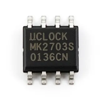
MK2304S-1LFT - 133MHz Zero-Delay Buffer | Renesas
N.º da peça: MK2304S-1LFT ✓ AtivoMK2304S-1LFT Visão geral
A zero-delay buffer is a clock and timing integrated circuit that uses phase-locked-loop techniques to reproduce a clock edge with very low delay. Unlike a passive buffer, it can compensate for clock distribution delay and provide a stable, low-skew output for sequential logic. The MK2304S-1LFT is therefore positioned within the clock buffer, PLL, and clock-generation hierarchy, where it supports high-speed clock routing across a board or between functional blocks.
The main electrical characteristics identify the part as a 133 MHz maximum-frequency, single-circuit clock buffer with CMOS output. Its 8-SOIC package provides a compact surface-mount implementation with a stated body width of 3.90 mm. The zero-delay architecture is particularly useful when the clock must reach multiple circuits without introducing significant edge-to-edge timing variation. Its single output arrangement makes it straightforward to use where one buffered clock reference is required rather than a multi-output fanout network.
Typical applications include processor and FPGA clock conditioning, memory interface clock distribution, communications equipment, test and measurement systems, and other digital platforms operating below or at 133 MHz. In these systems, the buffer can isolate or reshape a source clock while preserving the timing relationship needed by downstream logic. The 3.3 V CMOS operating environment also allows integration with common 3.3 V digital logic families when timing, voltage, and loading conditions are checked together.
Designers should verify input clock amplitude, rise and fall times, output loading, board skew, and downstream input thresholds against the manufacturer datasheet. The package requires normal decoupling and careful clock routing, while transmission-line effects may become relevant on longer traces. This page combines the verified device identity, package information, timing role, drop-in reference information, and practical selection guidance for engineers evaluating the MK2304S-1LFT in clock-distribution designs.
Alternativas drop-in para MK2304S-1LFT — mesmo encapsulamento, compatível pino a pino. Peças de encapsulamento diferente que exigem retrabalho na PCB são excluídas.
MK2304S-2ILFTR
✅ Drop-In📋 Alternativa de referência (fora do catálogo)
MK2304S-1LFT Especificações
| Device Type | Zero-delay buffer |
| PLL | Yes |
| Input Type | Clock |
| Tipo de saída | CMOS |
| Maximum Frequency | 133 MHz |
| Number of Circuits | 1 circuit |
| Input-to-Output Ratio | 1X |
| Supply Voltage Range | 3 V to 3.6 V |
| Encapsulamento | 8-SOIC |
| Package Width | 3.90 mm |
| Tipo de montagem | Surface mount |
Guia de Configuração de Pinos do MK2304S-1LFT 3.90 mm
Configuração de pinos para MK2304S-1LFT (pacote 3.90 mm). A numeração dos pinos, funções e diagramas de conexão estão definidos no datasheet do fabricante. Consulte-o para o footprint exato e diretrizes de soldagem.

Nenhum dado detalhado de pinagem disponível para MK2304S-1LFT.
Consulte a ficha técnica para a configuração completa dos pinos.
Aplicações típicas
MK2304S-1LFT é adequado para 6 aplicaçãos: FPGA Clock Distribution, Processor Reference Clock, Communications Equipment, Memory Interface Clocking, Test and Measurement Instrumentation, Industrial Control Logic.
FPGA Clock Distribution
The MK2304S-1LFT is appropriate for conditioning a clock before it reaches an FPGA or other high-speed digital load. Its PLL-based zero-delay architecture is designed to reproduce the clock edge with low skew, while the single CMOS output is suited to a single destination or fanout point. For a 100 MHz FPGA interface, the 133 MHz maximum operating frequency provides frequency headroom. Confirm the FPGA input threshold, allowed jitter, clock capacitance, and edge-rate limits, then place the buffer close enough to the destination to minimize trace propagation variation.
Recomendado
Processor Reference Clock
Use the MK2304S-1LFT to condition a low-skew clock reference for processors, controllers, and other synchronous digital logic. Its 133 MHz operating capability accommodates common reference-clock rates below that limit, while the 3 V to 3.6 V supply range supports 3.3 V systems. The buffer is particularly useful when source impedance or clock-tree loading would otherwise contribute excessive delay. Validate amplitude, duty-cycle limits, output drive, and receiver loading before insertion into a production topology.
Recomendado
Communications Equipment
The MK2304S-1LFT can support clock routing in communications equipment where low-skew edge reproduction matters at clock rates up to 133 MHz. Its CMOS output and zero-delay architecture suit digital logic blocks operating in a compatible 3.3 V domain. In such systems, the buffer helps isolate the source clock from downstream loading and can reduce accumulated clock-tree delay. Keep the output trace short, provide a solid ground reference, and verify the receiver's clock tolerance and maximum input capacitance.
Recomendado
Memory Interface Clocking
The zero-delay buffer can be evaluated for clock distribution associated with synchronous memory and related high-speed digital interfaces. At frequencies up to 133 MHz, it offers low-skew edge reproduction and a CMOS output for compatible receivers. The main design requirement is to keep clock and data topology in the same clock domain and to avoid adding long, poorly terminated clock branches. Confirm setup and hold timing at every receiver because a low-skew source clock does not eliminate data-bus timing constraints.
Recomendado
Test and Measurement Instrumentation
The MK2304S-1LFT is useful in instrumentation and test systems that require a low-skew clock for acquisition, sequencing, or control logic. The 133 MHz maximum frequency and 3.3 V operating range make it practical for intermediate-speed digital sections. A clock buffer can generate a more controlled edge when a source oscillator or divider has unsuitable drive or loading characteristics. Evaluate output jitter, slew rate, and cumulative board skew with the complete instrument timing chain rather than judging the buffer in isolation.
Recomendado
Industrial Control Logic
The MK2304S-1LFT fits industrial control boards that distribute a common clock among sequential logic, counters, communications interfaces, or data-conversion circuits. Its low-skew zero-delay function supports consistent edge arrival when operating below 133 MHz, and the 8-SOIC package supports conventional surface-mount assembly. For factory equipment, account for ambient temperature, ground return paths, and nearby switching noise. The buffer should not be expected to correct jitter or waveform problems originating at the oscillator or upstream divider.
Recomendado
Resumo dos produtos recomendados
Dados de referência de engenharia para MK2304S-1LFT — comparação, orientação de projeto e informações de conformidade.
Guia de seleção
Comparação com alternativas
| Parâmetro | Este produto | MK2304S-2ILFTR |
|---|---|---|
| Package | 8-SOIC | 8-SOIC - related same-family package |
| Brand | Renesas Electronics | Renesas Electronics |
Principais diferenciais
- PLL-based zero-delay operation (vs MK2304S-2ILFTR)
- Single CMOS clock output (vs MK2304S-2ILFTR)
- Defined 3.3 V operating range (vs MK2304S-2ILFTR)
Notas de projeto
Place the MK2304S-1LFT near the clock receiver when trace length, connector transitions, or fanout could distort edge timing. Maintain a continuous ground reference under the clock route, avoid long stubs, and match clock topology to the source and receiver impedances. Although the device operates up to 133 MHz, the practical bandwidth demand rises sharply near that limit, so edge-rate and topology checks remain essential.
Follow the manufacturer datasheet for power and decoupling connections. Place the required supply capacitor close to the device's supply pin, keep the return path short, and route the clock output away from high-current switching nodes. Confirm the 8-SOIC footprint and pin-one orientation against the package drawing before fabrication, and check that the assembly process matches the manufacturer's handling recommendations.
Do not select this buffer solely by its 133 MHz headline frequency. Check input amplitude, duty cycle, rise and fall time, output loading, propagation delay, skew, and downstream receiver thresholds. A source clock that is already noisy or operates outside the input limits will not be corrected by the PLL-based buffer. Validate the complete source-to-receiver clock path under worst-case supply, temperature, and loading conditions.
Informações de conformidade
Compliance status is not explicitly stated in the manufacturer and distributor records for this device. The part is a general-purpose clock and timing IC, so AEC-Q100 qualification is not indicated.