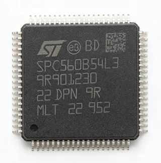
SC56F826BU80AE - 16-bit DSP, 80MHz, 32KB Flash MCU | NXP
N.º da peça: SC56F826BU80AE ✗ Fim de vida| Qtd. | Preço unitário | Total |
|---|---|---|
| 1 | $28.5 | $28,50 |
| 10 | $25.65 | $256,50 |
| 100 | $22.8 | $2.280,00 |
| 500 | $20.52 | $10.260,00 |
| 1.000 | $18.95 | $18.950,00 |
SC56F826BU80AE Visão geral
A Digital Signal Controller (DSC) is a hybrid semiconductor device that merges the deterministic, low-latency peripheral architecture of a microcontroller with the multiply-accumulate (MAC) throughput of a Digital Signal Processor (DSP). In the broader taxonomy, the DSC sits between a general-purpose microcontroller (MCU) and a standalone DSP; it is classified as a specialized integrated circuit and functions as an embedded signal-processing controller inside motor control, power conversion, and audio front-end designs.
Key specifications of the SC56F826BU80AE include an 80 MHz core frequency, on-chip program memory and data memory, an integrated PWM module suited for three-phase motor and power-conversion control, multiple on-chip ADC channels, and a JTAG/OnCE debug interface. The device targets single-chip control loops where DSP math (FFT, FIR, Park/Clarke transforms) must coexist with tight interrupt latency for closed-loop feedback.
Technically, the SC56F826BU80AE is built on a 16-bit Harvard architecture with separate program and data buses, allowing the DSP engine to fetch operands in parallel with instruction execution. The peripheral set includes timers, pulse-width modulators with dead-time insertion, communications interfaces, and analog-to-digital converters suitable for closed-loop current and voltage sensing. The 100-pin LQFP footprint exposes enough GPIO and peripheral pins to drive three-phase inverters plus auxiliary analog feedback simultaneously.
Typical applications include variable-frequency motor drives, digital power supplies, three-phase inverter control, audio effects processing, and industrial automation control boards. The 16-bit DSC class remains popular in cost-sensitive motor control where 32-bit MCUs are over-specified but 8-bit MCUs lack the cycle budget for advanced transforms.
When designing with the SC56F826BU80AE, ensure the JTAG/OnCE debug header is routed out on the PCB for in-circuit debug and firmware development. Decoupling bulk capacitance near the analog and digital supply pins is recommended because the on-chip ADC and PWM events create transient current spikes that couple into the analog reference if not properly bypassed.
This page synthesizes distributor pricing, drop-in alternatives, and practical design notes for engineers evaluating the SC56F826BU80AE - information not consolidated in any single manufacturer datasheet.
Alternativas drop-in para SC56F826BU80AE — mesmo encapsulamento, compatível pino a pino. Peças de encapsulamento diferente que exigem retrabalho na PCB são excluídas.
Variantes desta série
Modelos da mesma série compatíveis como drop-in com SC56F826BU80AE (mesmo formato e footprint) — diferindo em Debug Interface, Package.
Ferramenta de comparação rápida — selecione peças alternativas para comparação lado a lado:
SC56F826BU80A
✅ Drop-In📋 Alternativa de referência (fora do catálogo)
DSP56F826BU80E
✅ Drop-In✓ Em estoque
$1 / unidade
Ver ficha técnica →SC56F826BU80AE Classificações máximas e características elétricas
| Product Type | 16-bit Digital Signal Controller (DSC) |
| Core Architecture | 16-bit Harvard (DSP + MCU hybrid) |
| Core Clock Speed | 80 MHz |
| Encapsulamento | LQFP-100 |
| Contagem de pinos | 100 |
| Faixa de temperatura de operação | -40C to +85C (industrial, extended) |
| PWM Module | Yes (motor/power-control oriented) |
| On-chip ADC | Yes (multi-channel) |
| Debug Interface | JTAG / OnCE |
| Tipo de montagem | Surface Mount |
| Status RoHS | Compliant |
| Lead-Free | Yes |
| Manufacturer | NXP Semiconductors (formerly Freescale Semiconductor) |
| Series / Family | DSP56F826 / 56F8xx |
Guia de Configuração de Pinos do SC56F826BU80AE lqfp-100
Configuração de pinos para SC56F826BU80AE (pacote lqfp-100). Este CI digital inclui GPIO, interfaces de comunicação (UART, SPI, I2C) e pinos de alimentação. Consulte o datasheet do fabricante para funções alternativas dos pinos e opções de configuração. Essencial para projeto de sistemas embarcados e layout de PCB.
Nenhum dado detalhado de pinagem disponível para SC56F826BU80AE.
Consulte a ficha técnica para a configuração completa dos pinos.
Aplicações típicas
SC56F826BU80AE é adequado para 6 aplicaçãos: Three-Phase Motor Drive / Variable Frequency Drive, Digital Switch-Mode Power Supply (SMPS) Control, Audio Effects Processing, Industrial Automation Controller, Solar Inverter / Renewable Power Control, Uninterruptible Power Supply (UPS) Control.
Three-Phase Motor Drive / Variable Frequency Drive
The SC56F826BU80AE's 80 MHz 16-bit DSP core, integrated PWM module with dead-time insertion, and multi-channel ADC make it a strong fit for three-phase AC induction and PMSM motor drives. Field-oriented-control loops typically execute Park/Clarke/SVPWM transforms in a single PWM period of 50-100 microseconds; at 80 MHz (12.5 ns per instruction cycle) the SC56F826 has enough throughput to leave margin for current-loop and speed-loop closure simultaneously. The LQFP-100 footprint exposes enough GPIO for three-phase gate driver enable signals plus Hall/encoder feedback and analog current sensing. Unlike 32-bit Cortex-M alternatives, the 56F826 retains deterministic interrupt latency required by hard real-time motor control. Engineers typically pair it with NXP MC33HB2000 or similar three-phase gate drivers.
Recomendado
Digital Switch-Mode Power Supply (SMPS) Control
The SC56F826BU80AE is well-suited for digitally controlled SMPS designs where the on-chip PWM, ADC, and DSP throughput can implement peak current-mode or average current-mode control in real time. At 80 MHz the DSC can sample ADC, compute the control law (PI or sliding-mode), and update PWM duty cycle all within a 100 kHz switching period (10 microseconds). The LQFP-100 footprint allows analog feedback channels for primary current/voltage sensing plus isolated secondary-side feedback. Designers moving from analog UC3842-style controllers benefit from the 56F826's firmware-defined loop dynamics. Pin-to-pin compatibility with the SC56F826BU80A enables legacy design reuse while firmware migration to the 56F8xxx family is evaluated.
Recomendado
Audio Effects Processing
For audio front-ends requiring real-time effects (reverb, EQ, dynamics), the SC56F826BU80AE delivers enough MAC throughput to process two-channel audio at 48 kHz sample rates with headroom for additional DSP blocks. The 16-bit fixed-point architecture suits audio's native integer representation without scaling overhead. On-chip PWM can drive Class-D amplifier outputs directly, reducing external component count. The 56F826's interrupt latency is low enough to maintain glitch-free audio output even when the CPU is busy with effects computation. Legacy audio products built on the 56F826 family continue to ship because firmware development investment outweighs migration cost.
Recomendado
Industrial Automation Controller
Industrial automation and process-control boards benefit from the SC56F826BU80AE's industrial temperature grade (-40C to +85C), PWM peripheral, and multi-channel ADC in a single LQFP-100 device. PLC expansion modules, machine-vision front-ends, and conveyor controllers use the 56F826 for sensor acquisition plus actuator PWM drive in a deterministic loop. The JTAG/OnCE debug interface enables in-circuit firmware development on the production line. Compared with 32-bit Cortex-M0 alternatives, the 56F826 retains 16-bit math efficiency important for legacy control algorithms. Rochester Electronics continues to support industrial customers with NRND inventory.
Recomendado
Solar Inverter / Renewable Power Control
Solar micro-inverters and grid-tied photovoltaic converters use the SC56F826BU80AE's DSP throughput for MPPT (Maximum Power Point Tracking) algorithms and grid-synchronization PLL math. At 80 MHz the core computes incremental-conductance MPPT within a 100 ms scan cycle and updates PWM duty cycle for the boost or full-bridge stage in real time. The multi-channel ADC reads panel voltage, panel current, and grid voltage simultaneously for synchronized control. AEC-style reliability at industrial temperature grades makes the part suitable for outdoor inverter enclosures. The 100-pin LQFP footprint supports the analog feedback count required by these topologies.
Recomendado
Uninterruptible Power Supply (UPS) Control
UPS designs use the SC56F826BU80AE to run inverter control loops, battery charging algorithms, and AC-line synchronization simultaneously. The 16-bit DSP MAC throughput handles RMS voltage computation and battery-state-of-charge math in real time, while PWM channels drive the inverter bridge. Industrial temperature grade and LQFP-100 pin count accommodate the analog sensing required for AC-line, DC-bus, and battery current monitoring. Legacy UPS designs built on 56F826 firmware can extend service life through authorized Rochester Electronics inventory while planning eventual migration to 56F8xxx.
Recomendado
Resumo dos produtos recomendados
Dados de referência de engenharia para SC56F826BU80AE — comparação, orientação de projeto e informações de conformidade.
Guia de seleção
Comparação com alternativas
| Parâmetro | Este produto | SC56F826BU80A | DSP56F826BU80 |
|---|---|---|---|
| Package | LQFP-100 | LQFP-100 - same | LQFP-100 - same |
| Brand | NXP Semiconductors | NXP Semiconductors - same | NXP Semiconductors - same (Freescale legacy branding) |
| Core Architecture | 16-bit DSC (DSP+MCU) | 16-bit DSC (DSP+MCU) | 16-bit DSC (DSP+MCU) |
| Core Clock Speed | 80 MHz | 80 MHz | 80 MHz |
| Lifecycle Status | NRND | NRND | NRND (older Freescale branding) |
| PWM Module | Yes (motor/power oriented) | Yes | Yes |
| On-chip ADC | Yes (multi-channel) | Yes | Yes |
| Debug Interface | JTAG / OnCE | JTAG / OnCE | JTAG / OnCE |
Principais diferenciais
- Identical silicon with industrial temperature suffix designation (vs SC56F826BU80A)
- Modern NXP branding versus legacy Freescale branding (vs DSP56F826BU80)
- NRND status with continued authorized distributor inventory (vs EOL SC56F826 variants)
Notas de projeto
Estimated: at 80 MHz full-activity in LQFP-100 with typical industrial ambient (25C), the SC56F826BU80AE dissipates between 0.4W and 0.8W depending on peripheral activity (PWM switching, ADC sampling, GPIO toggling). The LQFP-100 package has a higher thermal resistance than QFN alternatives (theta_JA typically ~50 C/W on a 4-layer JEDEC board). For continuous full-load operation, ensure a minimum 1 square inch of unbroken ground plane beneath the part to stay below 70C junction rise. Forced-air cooling is recommended in enclosed motor-drive cabinets where ambient may exceed 60C.
Place bulk decoupling capacitors (4.7uF to 10uF ceramic plus 100uF electrolytic) within 5 mm of the SC56F826BU80AE VDD pins. Separate analog and digital ground planes should be joined at a single point beneath the DSC to prevent ADC reference corruption from PWM-induced ground bounce. Route the JTAG/OnCE debug header to a 2x5 0.1-inch header on the PCB edge - this enables in-circuit firmware debugging without removing the MCU from the board. Keep ADC analog traces away from PWM gate-driver traces to minimize capacitive coupling.
Estimated: the SC56F826BU80AE's 16-bit ADC achieves best noise performance when the analog supply is bypassed with separate ferrite-bead-isolated rails from the digital VDD. PWM edges with 1-2 ns rise times create broadband harmonics that couple into adjacent ADC input traces - route PWM outputs on one PCB layer and ADC inputs on a different layer with a ground plane sandwich. Add a 100 ohm RC low-pass filter on each ADC input if the source impedance exceeds 5 kohm to prevent input-current-induced settling errors. The OnCE debug clock should be gated during sensitive ADC conversions if spurious coupling is observed.
Because the SC56F826BU80AE is NRND, sourcing teams should plan an obsolescence mitigation strategy now - either stockpile via authorized distributor Rochester Electronics, qualify a 56F8xxx successor, or accept lifetime-buy risk. Do not assume the 'A' suffix (without 'E') part has identical temperature grade - confirm the operating range in the 56F826 family datasheet before substituting. Verify that the JTAG/OnCE header pinout matches the Freescale/NXP standard (not all 56F8xxx family members share identical debug pinouts). Finally, ensure the firmware was originally built against the 56F826 core's interrupt vector layout - porting to a newer NXP DSC family requires vector remapping.
Informações de conformidade
RoHS-compliant and lead-free per NXP/Freescale product page. AEC-Q100 not applicable (industrial-grade DSC, not automotive-qualified). Halogen-free status not verified in the provided data. NRND lifecycle per latest distributor indicators (Rochester Electronics holding stock on DigiKey Marketplace as of 2026-10-16).