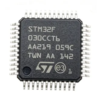
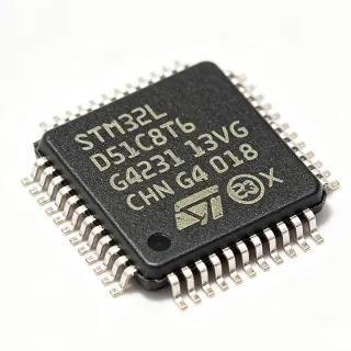
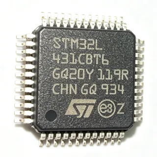
STM32F334C8T6 - 32-bit ARM Cortex-M4 MCU with FPU | STMicroelectronics
N.º da peça: STM32F334C8T6 ✓ Ativo| Qtd. | Preço unitário | Total |
|---|---|---|
| 1 | $6.5 | $6,50 |
| 10 | $5.85 | $58,50 |
| 100 | $5.2 | $520,00 |
| 500 | $4.68 | $2.340,00 |
| 1.000 | $4.16 | $4.160,00 |
STM32F334C8T6 Visão geral
A microcontroller (MCU) is a compact integrated circuit designed to govern a specific operation in an embedded system. It contains a processor core, memory, and programmable input/output peripherals. The STM32F334C8T6 belongs to the STM32F3 family, which is optimized for mixed-signal control applications, combining a high-performance ARM Cortex-M4 core with advanced analog peripherals such as high-resolution timers, comparators, and operational amplifiers.
Key features include a 72 MHz ARM Cortex-M4 core with FPU, 64 KB Flash, 12 KB SRAM, and a rich set of peripherals: 5x USART, 2x SPI, 2x I2C, 1x USB 2.0 FS, 1x CAN, 12-bit ADC with up to 21 channels, 12-bit DAC, and advanced 16-bit timers with dead-time generation for motor control. The device also includes a high-resolution timer (HRTIM) with 217 ps resolution, making it ideal for digital power conversion and lighting applications.
The STM32F334C8T6 integrates a nested vectored interrupt controller (NVIC), a memory protection unit (MPU), and a single-cycle multiply and hardware divide. The FPU accelerates mathematical operations for control algorithms, while the advanced analog peripherals reduce external component count. The device operates from 2.0V to 3.6V supply and supports a temperature range of -40°C to +85°C.
Typical applications include field-oriented control (FOC) of brushless DC motors, digital power supplies (buck, boost, flyback), solar inverters, LED lighting, and industrial automation. The high-resolution timer and fast ADC enable precise current and voltage sensing for closed-loop control.
When designing with this MCU, ensure proper decoupling of the VDD pins with 100 nF capacitors and a 4.7 uF bulk capacitor. The VDDA pin must be connected to a clean analog supply, and the VREF+ pin should be filtered to achieve optimal ADC accuracy. For motor control, use the HRTIM and ADC in interleaved mode to minimize latency.
Alternativas drop-in para STM32F334C8T6 — mesmo encapsulamento, compatível pino a pino. Peças de encapsulamento diferente que exigem retrabalho na PCB são excluídas.
Ferramenta de comparação rápida — selecione peças alternativas para comparação lado a lado:
STM32F334C8T7
✅ Drop-In ⚠️ Especificações não verificadas📋 Alternativa de referência (fora do catálogo)
STM32F334C6T6
✅ Drop-In ⚠️ Especificações não verificadas📋 Alternativa de referência (fora do catálogo)
STM32F334C4T6
✅ Drop-In ⚠️ Especificações não verificadas📋 Alternativa de referência (fora do catálogo)
STM32F303C8T6
✅ Drop-In ⚠️ Especificações não verificadas📋 Alternativa de referência (fora do catálogo)
STM32F334C8T6 Classificações máximas e características elétricas
| Core | ARM Cortex-M4 with FPU |
| Maximum Clock Speed | 72 MHz |
| Flash Memory | 64 KB |
| SRAM | 12 KB |
| Tensão de alimentação | 2.0 V to 3.6 V |
| Temperatura de operação | -40C to +85C |
| Encapsulamento | LQFP-48 (7x7 mm) |
| Tipo de montagem | Surface Mount |
| Number of I/Os | 37 |
| ADC Resolution | 12-bit |
| ADC Channels | 21 |
| DAC Resolution | 12-bit |
| DAC Channels | 1 |
| Timers | Advanced 16-bit timers with dead-time generation |
| High-Resolution Timer | 217 ps resolution |
| Communication Interfaces | 5x USART, 2x SPI, 2x I2C, 1x USB 2.0 FS, 1x CAN |
| Status RoHS | Compliant |
Configuração de pinos do STM32F334C8T6
| Pino 1 | VBAT — Battery backup supply |
| Pino 2 | PC13 — GPIO / RTC |
| Pino 3 | PC14 — GPIO / OSC32_IN |
| Pino 4 | PC15 — GPIO / OSC32_OUT |
| Pino 5 | PF0 — GPIO / OSC_IN |
| Pino 6 | PF1 — GPIO / OSC_OUT |
| Pino 7 | NRST — Reset |
| Pino 8 | VSSA — Analog ground |
| Pino 9 | VDDA — Analog power supply |
| Pino 10 | PA0 — GPIO / ADC_IN0 |
| Pino 11 | PA1 — GPIO / ADC_IN1 |
| Pino 12 | PA2 — GPIO / USART2_TX |
| Pino 13 | PA3 — GPIO / USART2_RX |
| Pino 14 | PA4 — GPIO / DAC_OUT1 |
| Pino 15 | PA5 — GPIO / DAC_OUT2 |
| Pino 16 | PA6 — GPIO / TIM1_CH1 |
| Pino 17 | PA7 — GPIO / TIM1_CH2 |
| Pino 18 | PB0 — GPIO / TIM1_CH3 |
| Pino 19 | PB1 — GPIO / TIM1_CH4 |
| Pino 20 | PB2 — GPIO / BOOT1 |
| Pino 21 | PB10 — GPIO / I2C2_SCL |
| Pino 22 | PB11 — GPIO / I2C2_SDA |
| Pino 23 | PB12 — GPIO / SPI2_NSS |
| Pino 24 | PB13 — GPIO / SPI2_SCK |
| Pino 25 | PB14 — GPIO / SPI2_MISO |
| Pino 26 | PB15 — GPIO / SPI2_MOSI |
| Pino 27 | PA8 — GPIO / MCO |
| Pino 28 | PA9 — GPIO / USART1_TX |
| Pino 29 | PA10 — GPIO / USART1_RX |
| Pino 30 | PA11 — GPIO / USB_DM |
| Pino 31 | PA12 — GPIO / USB_DP |
| Pino 32 | PA13 — GPIO / SWDIO |
| Pino 33 | PA14 — GPIO / SWCLK |
| Pino 34 | PA15 — GPIO / JTDI |
| Pino 35 | PB3 — GPIO / JTDO |
| Pino 36 | PB4 — GPIO / NJTRST |
| Pino 37 | PB5 — GPIO / I2C1_SMBA |
| Pino 38 | PB6 — GPIO / I2C1_SCL |
| Pino 39 | PB7 — GPIO / I2C1_SDA |
| Pino 40 | BOOT0 — Boot mode selection |
| Pino 41 | PB8 — GPIO / CAN_RX |
| Pino 42 | PB9 — GPIO / CAN_TX |
| Pino 43 | VDD — Digital power supply |
| Pino 44 | VSS — Digital ground |
| Pino 45 | PC14 — GPIO / OSC32_IN |
| Pino 46 | PC15 — GPIO / OSC32_OUT |
| Pino 47 | PC13 — GPIO / RTC |
| Pino 48 | VBAT — Battery backup supply |
Aplicações típicas
STM32F334C8T6 é adequado para 6 aplicaçãos: Field-Oriented Control (FOC) of Brushless DC Motors, Digital Power Supplies (Buck, Boost, Flyback), Solar Inverters, LED Lighting, Industrial Automation, Test and Measurement Equipment.
Field-Oriented Control (FOC) of Brushless DC Motors
The STM32F334C8T6 is ideal for FOC of BLDC motors due to its high-resolution timer (HRTIM) with 217 ps resolution and fast 12-bit ADC. The HRTIM generates precise PWM signals for three-phase inverters, while the ADC samples phase currents with minimal latency. The FPU accelerates Clarke and Park transforms, enabling efficient real-time control. In a typical FOC application, the MCU reads current sensors via the ADC, computes the rotor position using Hall sensors or encoders, and updates PWM duty cycles at a rate of 20 kHz. The advanced timers provide dead-time insertion to prevent shoot-through in the inverter bridge. Compared to general-purpose MCUs, the STM32F334C8T6 reduces CPU load by offloading PWM generation to hardware, allowing more headroom for complex control algorithms. Designers should ensure proper grounding and shielding of analog inputs to maintain ADC accuracy.
Recomendado
Digital Power Supplies (Buck, Boost, Flyback)
The STM32F334C8T6 excels in digital power conversion due to its HRTIM, which provides high-resolution PWM for precise voltage regulation. The HRTIM's 217 ps resolution allows fine control of duty cycle, reducing output ripple. The fast ADC enables high-bandwidth voltage and current sensing for closed-loop control. In a typical buck converter application, the MCU reads the output voltage via a resistor divider, compares it to a reference, and adjusts the PWM duty cycle to maintain regulation. The HRTIM's fault inputs provide hardware protection against overcurrent and overvoltage. The FPU accelerates PID control loops, enabling high switching frequencies up to 1 MHz. Compared to analog controllers, the digital approach offers flexibility in tuning and monitoring. Designers should pay attention to the ADC sampling time and PWM update rate to ensure stability.
Recomendado
Solar Inverters
The STM32F334C8T6 is well-suited for solar inverters, where it manages maximum power point tracking (MPPT) and DC-AC conversion. The HRTIM generates high-frequency PWM for the inverter bridge, while the ADC monitors solar panel voltage and current. The FPU accelerates MPPT algorithms, such as perturb and observe, to maximize energy harvest. In a typical solar inverter, the MCU controls a boost converter to step up the panel voltage and an H-bridge to produce AC output. The HRTIM's dead-time generation ensures safe switching of the bridge. The device's wide operating temperature range (-40°C to +85°C) makes it suitable for outdoor installations. Compared to dedicated solar inverter ICs, the STM32F334C8T6 offers programmability for different topologies. Designers should implement robust protection features, such as overvoltage and overcurrent detection, using the HRTIM fault inputs.
Recomendado
LED Lighting
The STM32F334C8T6 is used in advanced LED lighting systems for dimming and color control. The HRTIM provides high-resolution PWM for precise brightness control, while the ADC monitors LED current for constant-current regulation. The device supports multiple channels, enabling RGB color mixing. In a typical LED driver, the MCU generates PWM signals to control a buck converter, maintaining a constant current through the LED string. The HRTIM's high resolution minimizes flicker, even at low dimming levels. The FPU enables smooth color transitions and gamma correction. Compared to dedicated LED driver ICs, the STM32F334C8T6 offers flexibility for complex lighting effects. Designers should ensure proper thermal management, as LED drivers can dissipate significant power.
Recomendado
Industrial Automation
The STM32F334C8T6 is suitable for industrial automation, including PLCs, motor drives, and robotic controllers. Its rich set of communication interfaces (USART, SPI, I2C, CAN, USB) enables connectivity to sensors, actuators, and industrial networks. The advanced timers provide precise timing for motion control, while the ADC and DAC interface with analog sensors and actuators. In a typical PLC, the MCU reads digital inputs, executes logic, and drives outputs. The CAN interface allows communication with other controllers in a factory network. The device's robust design, with a wide temperature range and low power consumption, makes it reliable in harsh environments. Compared to dedicated PLC chips, the STM32F334C8T6 offers programmability and cost-effectiveness. Designers should implement proper isolation for industrial interfaces to protect the MCU from electrical noise.
Recomendado
Test and Measurement Equipment
The STM32F334C8T6 is used in test and measurement equipment, such as data loggers, signal generators, and power analyzers. Its high-resolution ADC and DAC enable accurate signal acquisition and generation. The FPU accelerates digital signal processing, such as filtering and FFT. In a typical data logger, the MCU samples analog signals at high speed, stores data in Flash, and communicates via USB. The HRTIM can generate precise trigger signals for synchronized measurements. The device's low power consumption is beneficial for battery-powered instruments. Compared to dedicated measurement ICs, the STM32F334C8T6 offers flexibility and integration. Designers should ensure a clean analog supply for the ADC to achieve high accuracy.
Recomendado
Resumo dos produtos recomendados
Dados de referência de engenharia para STM32F334C8T6 — comparação, orientação de projeto e informações de conformidade.
Guia de seleção
Comparação com alternativas
| Parâmetro | Este produto | STM32F334C8T7 | STM32F334C6T6 | STM32F334C4T6 | STM32F303C8T6 |
|---|---|---|---|---|---|
| Package | LQFP-48 | LQFP-48 | LQFP-48 | LQFP-48 | LQFP-48 |
| Brand | STMicroelectronics | STMicroelectronics | STMicroelectronics | STMicroelectronics | STMicroelectronics |
| Core | ARM Cortex-M4 with FPU | ARM Cortex-M4 with FPU | ARM Cortex-M4 with FPU | ARM Cortex-M4 with FPU | ARM Cortex-M4 with FPU |
| Maximum Clock Speed | 72 MHz | 72 MHz | 72 MHz | 72 MHz | 72 MHz |
| Flash Memory | 64 KB | 64 KB | 32 KB | 16 KB | 64 KB |
| SRAM | 12 KB | 12 KB | 12 KB | 12 KB | 16 KB |
| High-Resolution Timer (HRTIM) | Yes (217 ps) | Yes (217 ps) | Yes (217 ps) | Yes (217 ps) | No |
| Operating Temperature Range | -40C to +85C | -40C to +105C | -40C to +85C | -40C to +85C | -40C to +85C |
Principais diferenciais
- High-resolution timer (HRTIM) with 217 ps resolution (vs STM32F303C8T6)
- Extended temperature range option (STM32F334C8T7) (vs STM32F334C8T6)
- Pin-compatible family with multiple Flash sizes (vs STM32F334C6T6)
Notas de projeto
Decouple each VDD pin with a 100 nF ceramic capacitor placed as close as possible to the pin. Additionally, use a 4.7 uF bulk capacitor on the main VDD rail. The VDDA pin must be connected to a clean analog supply, and VREF+ should be filtered with a 1 uF capacitor to ensure ADC accuracy. For battery-powered designs, connect VBAT to a backup battery or tie it to VDD through a diode.
For optimal ADC performance, route analog signals away from digital traces and use a ground plane. Place the crystal oscillator (if used) close to the OSC_IN/OSC_OUT pins with load capacitors as specified in the datasheet. For motor control applications, keep the power stage separate from the MCU to minimize noise coupling. Use a 4-layer PCB with dedicated power and ground planes for best EMC performance.
Ensure the BOOT0 pin is properly configured to select the correct boot mode. If using SWD for programming, connect PA13 (SWDIO) and PA14 (SWCLK) with pull-up/pull-down resistors as recommended. Do not exceed the absolute maximum ratings for supply voltage (3.6V) or I/O pins. For high-resolution timer applications, verify the HRTIM clock source and configuration to avoid unexpected PWM behavior.
Informações de conformidade
RoHS compliant per STMicroelectronics product page. Not AEC-Q100 qualified; for automotive, consider STM32F334C8T7 with extended temperature range.