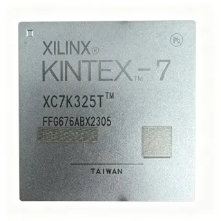
XC5VLX50-2FF676I - 440 I/O Virtex-5 LX FPGA | AMD
N.º da peça: XC5VLX50-2FF676I ✗ Fim de vidaXC5VLX50-2FF676I Visão geral
A field-programmable gate array is a programmable semiconductor in which configurable logic blocks, routing resources, block RAM, digital signal processing resources, input/output resources, and clock-management circuits are interconnected through user-programmed configuration data. In the product hierarchy, an FPGA sits above a programmable logic device and becomes a reconfigurable digital system-on-chip. Virtex-5 LX devices target high-performance programmable logic, parallel processing, interface bridging, embedded control, and signal-processing systems that require substantial logic and I/O resources.
The XC5VLX50-2FF676I combines 440 I/O with a 676-ball package, providing high connectivity for board-to-board interfaces, memory connections, network ports, video or image-processing links, and high-speed control fabrics. Its industrial temperature designation supports systems intended for controlled industrial environments. The ASMBL architecture uses column-based logic organization to support high-performance routing and predictable implementation of large digital designs. The device also carries 46,080 registers, which provide substantial sequential and datapath resources.
The -2 suffix denotes the device performance grade, while the FF676 package identifier corresponds to the 676-ball surface-mount FCBGA footprint. Pin assignment, differential I/O standards, configuration requirements, power sequencing, and decoupling must be implemented according to the manufacturer datasheet. Programming is performed through the supported configuration interface, and the resulting circuit is defined by the bitstream loaded into the FPGA configuration memory. This makes the same physical device usable for different logic functions when the board, configuration memory, and design are changed.
Typical uses include industrial control and automation, telecommunications interface equipment, test and measurement systems, high-speed data acquisition, network packet processing, video infrastructure, embedded signal processing, and defense or aerospace electronics requiring programmable logic. Its large I/O count is particularly useful when a design must connect multiple buses, external memories, converters, and clock sources without relying on several smaller programmable devices.
PCB implementation requires a dense BGA escape strategy, continuous power and ground planes, careful via-in-pad or fanout construction, and decoupling close to the device. Designers should follow the manufacturer’s pinout, package, power, configuration, and decoupling guidance rather than relying only on the device family name. The physical footprint and full pin map must also be cross-checked before any replacement is approved.
This product page combines the exact package, architecture, resource, interface, and ordering identifiers with application guidance, replacement constraints, and engineering-focused design notes. It also highlights why speed-grade, temperature-grade, and package suffixes must be compared individually before any board-level substitution is considered.
Alternativas drop-in para XC5VLX50-2FF676I — mesmo encapsulamento, compatível pino a pino. Peças de encapsulamento diferente que exigem retrabalho na PCB são excluídas.
Variantes desta série
Modelos da mesma série compatíveis como drop-in com XC5VLX50-2FF676I (mesmo formato e footprint) — diferindo em Device Type, Speed Grade.
XC5VLX50-2FF676C
✅ Drop-InConsulte o preço
Ver ficha técnica →XC5VLX50-3FFG676C
✅ Drop-In📋 Alternativa de referência (fora do catálogo)
XC5VLX50-2FF677C
✅ Drop-In📋 Alternativa de referência (fora do catálogo)
XC5VLX50-2FF676I Classificações máximas e características elétricas
| Device Type | Virtex-5 LX Field Programmable Gate Array (FPGA) |
| Architecture | Second-generation ASMBL column-based FPGA architecture |
| Logic Resource Identifier | 17,694,72? as listed in the exact product record; unit definition requires confirmation |
| Register Count | 46,080 registers |
| Input/Output Count | 440 I/O |
| Encapsulamento | 676-BBGA, FCBGA |
| Terminal Type | Ball |
| Package Shape | Square |
| Total Terminals | 676 terminals |
| Temperature Grade | Industrial grade |
| Speed Grade | -2 performance grade |
| Tipo de montagem | Surface mount |
Guia de Configuração de Pinos do XC5VLX50-2FF676I square
Configuração de pinos para XC5VLX50-2FF676I (pacote square). Este CI digital inclui GPIO, interfaces de comunicação (UART, SPI, I2C) e pinos de alimentação. Consulte o datasheet do fabricante para funções alternativas dos pinos e opções de configuração. Essencial para projeto de sistemas embarcados e layout de PCB.

Nenhum dado detalhado de pinagem disponível para XC5VLX50-2FF676I.
Consulte a ficha técnica para a configuração completa dos pinos.
Aplicações típicas
XC5VLX50-2FF676I é adequado para 6 aplicaçãos: Industrial Control and Automation, Telecommunications Interface Equipment, High-Speed Data Acquisition, Test and Measurement Systems, Network Packet Processing, Embedded Signal Processing.
Industrial Control and Automation
The XC5VLX50-2FF676I fits industrial controllers that need extensive I/O for sensors, actuator drivers, field buses, and machine-control logic. Its 440 I/O can reduce the number of companion programmable devices, while 46,080 registers provide substantial capacity for sequential control and datapath functions. The industrial temperature suffix makes it the relevant member when the assembly is intended for controlled industrial environments. Designers should partition the ball map among banks according to the required I/O standards, maintain uninterrupted power and ground planes, and verify timing margins against the -2 performance grade before release.
Recomendado
Telecommunications Interface Equipment
The XC5VLX50-2FF676I is suitable for telecommunications interface equipment requiring many parallel and serial connections plus configurable protocol logic. Its 440 I/O can support multiple backplane links, payload interfaces, memory buses, and control channels within one FPGA package. The second-generation ASMBL architecture and 46,080 registers give designers room to implement parallel packet processing, buffering, and interface adaptation. Before schematic release, verify every differential I/O requirement against the manufacturer pinout and account for the larger voltage, current, and temperature constraints associated with telecommunications equipment.
Recomendado
High-Speed Data Acquisition
The XC5VLX50-2FF676I can serve as the central programmable fabric in a parallel or mixed-signal data-acquisition system. Its 440 I/O provide substantial connectivity for ADC outputs, digital sensors, timing inputs, memory interfaces, and data-processing pipelines, while the 46,080 registers support counters, packetization, and channel multiplexing. The -2 speed grade is appropriate when design timing must be closed against that grade rather than a faster or slower variant. Layout engineers should control routing escape, provide low-impedance power distribution, and apply the manufacturer’s bank-specific decoupling and voltage rules.
Recomendado
Test and Measurement Systems
The XC5VLX50-2FF676I is well matched to modular test and measurement systems that combine pattern generation, timing control, acquisition, and analysis in one programmable device. Its 440 I/O allow multiple instrument channels, trigger signals, converters, and status lines to be connected without relying on a large network of fixed-function logic. The large register count supports counters, state machines, pipelines, and instrument-control logic. Engineers should reserve the manufacturer-specified configuration pins, preserve clean references and supplies, and validate signal-integrity behavior for every supported I/O standard used by the instrument.
Recomendado
Network Packet Processing
The XC5VLX50-2FF676I can implement packet classification, buffering, traffic shaping, and protocol conversion in a programmable network interface. Its 440 I/O provide substantial bandwidth for parallel packet buses, physical-layer device interfaces, memory, and management paths, while 46,080 registers support deep sequential datapaths and queues. The second-generation ASMBL column-based architecture is intended to support high-performance FPGA logic. Layout should use short return paths for clock and configuration signals, maintain continuous supply planes, and confirm whether the system timing closes against the -2 speed grade.
Recomendado
Embedded Signal Processing
The XC5VLX50-2FF676I supports embedded signal-processing systems that require flexible logic, substantial register capacity, and high external connectivity. Potential roles include filter control, sampling-clock management, digital correction, channel multiplexing, and accelerator interfacing. The 440 I/O permit direct connection to multiple converters, memories, and clock sources, while the 676-ball FCBGA provides a dense but well-defined integration point. Designers must consult the manufacturer tables for block RAM, DSP, clocking, and bank-supply details before assigning the device, and should preserve configuration access for production programming and field updates.
Recomendado
Resumo dos produtos recomendados
Dados de referência de engenharia para XC5VLX50-2FF676I — comparação, orientação de projeto e informações de conformidade.
Guia de seleção
Comparação com alternativas
| Parâmetro | Este produto | XC5VLX50-2FF676C | XC5VLX50-3FFG676C | XC5VLX50-2FF677C |
|---|---|---|---|---|
| Package | 676-BBGA, FCBGA | 676-BBGA, FCBGA | 676-BBGA, FCBGA | 677-BBGA, FCBGA |
| Brand | AMD | AMD | AMD | AMD |
| Device Family | Virtex-5 LX FPGA | Virtex-5 LX FPGA | Virtex-5 LX FPGA | Virtex-5 LX FPGA |
| Speed Grade | -2 | -2 | -3 | -2 |
| Temperature Grade | Industrial | Commercial | Commercial | Commercial |
| Terminal Count | 676 terminals | 676 terminals | 676 terminals | 677 terminals |
Principais diferenciais
- Industrial-grade ordering configuration (vs XC5VLX50-2FF676C)
- Faster documented speed-grade designation (vs XC5VLX50-3FFG676C)
- Exact 676-ball package code (vs XC5VLX50-2FF677C)
Notas de projeto
Treat the 676-ball FCBGA land pattern as a controlled-layout interface. Follow the manufacturer package drawing for ball locations, ball-map assignments, and recommended escape routing. Keep power and ground planes continuous, place local decoupling at the corresponding package balls, and provide a manufacturable via strategy that satisfies both electrical and assembly requirements.
Implement the manufacturer’s supply, bank, and power-sequence requirements before assigning any I/O standard. Because the target can expose 440 I/O, rails and ground references must be partitioned according to the ball map rather than grouped by schematic function. Validate startup, shutdown, sequencing, and current demands across every operating mode before releasing the power tree.
Reserve configuration and clock access near the package and keep sensitive routing short and referenced to a continuous plane. For high-speed user I/O, follow the bank-specific guidance for voltage references, impedance, and return paths. Do not infer pin equivalence from the 676 or 677 package number alone; compare every relevant ball assignment mechanically and electrically.
The most common substitution error is matching only the family and speed grade while overlooking the temperature suffix, ball map, or package code. XC5VLX50-2FF676C changes the temperature designation, XC5VLX50-3FFG676C changes the speed and temperature suffixes, and XC5VLX50-2FF677C changes the package identifier. Confirm timing, temperature, footprint, configuration, and supply requirements before approving any replacement.
Power integrity and thermal performance must be evaluated together in the assembled FCBGA. Use the manufacturer power data for the actual design utilization rather than a nominal device figure, and estimate junction temperature from the calculated dissipation and the applicable package and board thermal model. The large BGA footprint also requires attention to copper connectivity, via arrays, and enclosure airflow.
Informações de conformidade
The exact product records identify an industrial temperature grade but do not establish RoHS, REACH, AEC-Q100, lead-free, halogen-free, or conflict-minerals status.