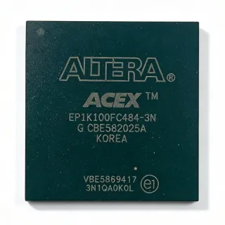
XC6SLX25T-2FG484I - 24,051-Cell FPGA | AMD/Xilinx
N.º da peça: XC6SLX25T-2FG484I ✓ AtivoXC6SLX25T-2FG484I Visão geral
A field-programmable gate array is a semiconductor device whose digital logic, interfaces, and signal-processing blocks are configured after manufacture. An FPGA belongs to the programmable-logic hierarchy, where configurable logic blocks, programmable I/O, embedded memory, DSP resources, and clock-management circuits implement control, networking, image-processing, and interface functions without requiring a custom ASIC mask set.
The XC6SLX25T family combines 24,051 logic cells with as many as 250 user I/O in a 23 mm by 23 mm, 1.0 mm-pitch FBGA package. Its 500 MHz internal-frequency figure indicates the device's stated internal operating range, while actual interface and design performance also depends on the selected clocking resources, I/O standards, speed grade, and external timing constraints.
The -2 speed designation places this device in the Spartan-6 performance range identified by AMD as one of the family's available grades. The T suffix identifies the Spartan-6 LXT family, and the FG484 package designation denotes the 484-ball surface-mount configuration. These suffix meanings should be confirmed against the AMD package and ordering documentation before a new PCB or procurement decision.
Typical applications include industrial control, video display bridges, embedded processing interfaces, network equipment, test systems, and general-purpose programmable logic. The combination of substantial logic capacity and a large I/O count makes the device useful for designs joining multiple interfaces, clock domains, memory resources, and real-time datapaths on one FPGA.
Design planning should begin with the AMD package pinout and Spartan-6 family documentation. Verify differential pairs, supply pins, configuration pins, clock-capable pins, and exposed thermal requirements against the exact -2 industrial ordering code. Use the manufacturer's package files to generate PCB land patterns and bonding constraints rather than relying on generic BGA dimensions.
This product record combines package, logic-capacity, temperature, speed-grade, and application information with a practical comparison of pin-compatible Spartan-6 options. It also highlights the electrical, thermal, and lifecycle checks required before using a mature FPGA family in a new industrial design.
Alternativas drop-in para XC6SLX25T-2FG484I — mesmo encapsulamento, compatível pino a pino. Peças de encapsulamento diferente que exigem retrabalho na PCB são excluídas.
Variantes desta série
Modelos da mesma série compatíveis como drop-in com XC6SLX25T-2FG484I (mesmo formato e footprint) — diferindo em Device Type, Package, Package Dimensions.
XC6SLX25T-2FGG484I
✅ Drop-In📋 Alternativa de referência (fora do catálogo)
XC6SLX25T-2FG484C
✅ Drop-InConsulte o preço
Ver ficha técnica →XC6SLX25T-2FGG484C
✅ Drop-In📋 Alternativa de referência (fora do catálogo)
XC6SLX25T-3FGG484I
✅ Drop-In📋 Alternativa de referência (fora do catálogo)
XC6SLX25T-N3FGG484I
✅ Drop-In📋 Alternativa de referência (fora do catálogo)
XC6SLX25T-2FG484I Classificações máximas e características elétricas
| Device Type | Field-Programmable Gate Array (FPGA) |
| FPGA Family | Spartan-6 LXT |
| Logic Cells | 24,051 cells |
| Configurable Logic Blocks | 1,879 CLBs |
| User I/O | Up to 250 I/O |
| Internal Frequency | 500 MHz |
| Speed Grade | -2 |
| Temperature Grade | Industrial, 0°C to 85°C |
| Encapsulamento | 484-ball FBGA |
| Package Dimensions | 23 mm × 23 mm |
| Ball Pitch | 1.0 mm |
| Process Technology | 45 nm CMOS |
| Tipo de montagem | Surface Mount |
| Terminal Type | Ball |
| Lead-Free Status | Lead-free package designation reported |
Guia de Configuração de Pinos do XC6SLX25T-2FG484I 23 mm × 23 mm
Configuração de pinos para XC6SLX25T-2FG484I (pacote 23 mm × 23 mm). Este CI digital inclui GPIO, interfaces de comunicação (UART, SPI, I2C) e pinos de alimentação. Consulte o datasheet do fabricante para funções alternativas dos pinos e opções de configuração. Essencial para projeto de sistemas embarcados e layout de PCB.

Nenhum dado detalhado de pinagem disponível para XC6SLX25T-2FG484I.
Consulte a ficha técnica para a configuração completa dos pinos.
Aplicações típicas
XC6SLX25T-2FG484I é adequado para 6 aplicaçãos: Industrial Control and Automation, Video Display and Interface Bridging, Network and Communications Equipment, Embedded Processor and Bus Interfacing, Test and Measurement Equipment, Aerospace and Defense Control Logic.
Industrial Control and Automation
The XC6SLX25T-2FG484I fits industrial control systems that combine deterministic logic, multiple external interfaces, and an operating range of 0°C to 85°C. Its 24,051 logic cells and as many as 250 I/O provide capacity for machine-control sequencing, sensor conditioning, actuator timing, communication bridging, and safety interlocks in one programmable device. The -2 speed grade provides useful timing margin for synchronized control loops, while the 484-ball package exposes more I/O than smaller packages. Designers should partition deterministic control paths from less critical supervisory logic, constrain clock domains, and reserve configuration and recovery functions for reliable field behavior.
Video Display and Interface Bridging
The XC6SLX25T-2FG484I is suitable for video-interface and display-bridging designs that require parallel logic, memory interfaces, and multiple data paths. Its 24,051-cell Spartan-6 LXT resource level can support timing conversion, frame-buffer control, pixel formatting, and ancillary-signal handling without a separate ASIC. The large 484-ball package offers up to 250 I/O, helping reduce the number of companion interface components when several buses or parallel streams must terminate on the FPGA. Practical designs must assign pins according to bank voltage rules, use clock-capable inputs correctly, and constrain all video and memory interfaces against the selected -2 timing limits.
Network and Communications Equipment
The XC6SLX25T-2FG484I can implement protocol conversion, packet processing, test loops, and interface isolation for network and communications equipment. Its 24,051 logic cells are useful for parallel-to-serial adaptation, buffering, framing logic, and multi-clock-domain control, while the 484-ball package offers substantial I/O connectivity. The industrial temperature range supports factory automation, instrumentation, and communications infrastructure that operates from 0°C to 85°C. For timing-sensitive links, engineers should use the clock-management resources, define clock-domain crossings explicitly, constrain source-synchronous interfaces, and verify I/O standards against each power bank voltage.
Embedded Processor and Bus Interfacing
The XC6SLX25T-2FG484I works well as a programmable companion to a processor or microcontroller in systems requiring custom peripherals, glue logic, and mixed bus arbitration. Its logic capacity can implement UART, SPI, parallel processor buses, memory controllers, DMA request logic, and interrupt coordination, while up to 250 I/O simplify connection to external data-acquisition and storage devices. The -2 speed grade supports demanding bus timing, but external interface performance remains dependent on pin placement and system-level timing budgets. Avoid relying solely on FPGA resources for functions requiring hard real-time guarantees, and verify all input thresholds against the selected power supply and I/O standard.
Test and Measurement Equipment
The XC6SLX25T-2FG484I is adaptable to automated test, instrumentation, and signal-generation systems that require parallel acquisition, pattern generation, timing control, and flexible interface routing. The 24,051-cell device can combine test sequencing, data capture, pattern generation, and communication logic in one FPGA, while the 484-ball package supports dense instrumentation connections. The 500 MHz internal-frequency figure provides a reference for the device's internal operating range, though usable signal-path bandwidth depends on I/O standards, pin locations, and timing closure. For measurement accuracy, separate analog front-end concerns from the FPGA and validate launch and capture timing at each interface.
Aerospace and Defense Control Logic
The XC6SLX25T-2FG484I can serve as the programmable logic core in aerospace, defense, and rugged embedded subsystems that need configurable sequencing, bus arbitration, data routing, and fault monitoring. Its Spartan-6 LXT architecture provides 24,051 logic cells, and the industrial-grade ordering suffix supports a 0°C to 85°C operating range. The device should not be treated as automatically qualified for flight or defense programs; qualification, radiation, reliability, and long-term availability requirements must be established separately. Engineers should implement redundant monitoring, configuration recovery, and deterministic resource allocation, then verify every electrical and environmental criterion against the program specification.
Dados de referência de engenharia para XC6SLX25T-2FG484I — comparação, orientação de projeto e informações de conformidade.
Guia de seleção
Comparação com alternativas
| Parâmetro | Este produto | XC6SLX25T-2FGG484I | XC6SLX25T-2FG484C | XC6SLX25T-2FGG484C | XC6SLX25T-3FGG484I | XC6SLX25T-N3FGG484I |
|---|---|---|---|---|---|---|
| Brand | AMD/Xilinx | AMD/Xilinx | AMD/Xilinx | AMD/Xilinx | AMD/Xilinx | AMD/Xilinx |
| Package | 484-FBGA | 484-BBGA - same package family | 484-BBGA - same package family | 484-BBGA - same package family | 484-BBGA - same package family | 484-BBGA - same package family |
| Device Type | Spartan-6 LXT FPGA | Spartan-6 LXT FPGA | Spartan-6 LXT FPGA | Spartan-6 LXT FPGA | Spartan-6 LXT FPGA | Spartan-6 LXT FPGA |
| Speed Grade | -2 | -2 | -2 | -2 | -3 | N3 |
Principais diferenciais
- Industrial-temperature coverage in the -2 performance configuration (vs XC6SLX25T-2FGG484C)
- Retains the familiar -2 speed grade for balanced performance (vs XC6SLX25T-3FGG484I)
- Large logic and I/O capacity for integrated industrial logic (vs XC6SLX25T-2FG484C)
Notas de projeto
Generate the PCB land pattern from the exact 484-ball package drawing and AMD package files. The package is listed as 23 mm by 23 mm with 1.0 mm ball pitch, but those dimensions alone do not define pad size, solder-mask opening, paste stencil, or assembly allowances. Validate the footprint against the selected -2 industrial ordering code and inspect the ball map for power, ground, configuration, clock-capable, and differential-pair assignments before fabrication.
Plan the power architecture directly from the Spartan-6 family documentation rather than treating all 484 balls as interchangeable signal connections. Separate core and I/O supply requirements, provide local high-frequency decoupling at the appropriate supply pins, and use a low-impedance distribution network for switching current. Estimated: if the total device dissipation is P watts and the effective board-to-ambient thermal resistance is R in °C/W, the estimated junction-temperature rise is P × R; substitute board-specific thermal data rather than assuming a generic value.
Assign clock-capable pins and differential pairs according to the AMD pin constraints before finalizing logic placement. Route clocks as short, continuous paths away from high-slew-rate outputs, keep clocking and configuration lines away from potential aggressors, and reserve pin locations required by memory or high-speed interfaces. The 500 MHz internal-frequency statement describes the device's internal range, not a guarantee that every external interface can operate at that rate.
Do not substitute a nearby 484-BBGA Spartan-6 device using package appearance alone. Confirm the exact XC6SLX25T suffix, -2 speed grade, I temperature suffix, configuration interface, I/O standards, and ball map. A change from I to C can reduce environmental suitability, while changing from -2 to -3 or N3 changes the performance grade and timing assumptions. Record the approved alternate MPN in the schematic and firmware documentation when substitution is unavoidable.
Informações de conformidade
The package information describes the related lead-free package designation. RoHS, REACH, AEC-Q100, halogen-free, and conflict-minerals status were not explicitly identified for this exact ordering code.