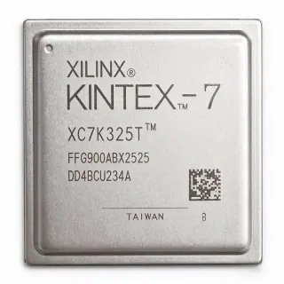
XCKU040-2FBVA900E - 530K-Cell Kintex UltraScale FPGA | AMD
N.º da peça: XCKU040-2FBVA900E ✓ AtivoXCKU040-2FBVA900E Visão geral
A field-programmable gate array is a programmable-logic device that can be configured after manufacture to implement digital functions. Within the product hierarchy, this Kintex UltraScale device combines configurable logic blocks, block RAM, DSP resources, programmable input/output, and high-speed transceivers. The UltraScale architecture places these resources in a fabric designed for scalable data paths, making the device suitable for systems that need more flexibility than a fixed application-specific integrated circuit.
Key device attributes include 530,250 logic cells, 30,300 logic-array blocks or configurable logic blocks, 468 user I/Os, and 21,606,000 bits of block RAM. The device uses a 0.95 V core supply and is manufactured in a 20 nm process. Its 900-ball flip-chip ball-grid-array package provides 31 mm by 31 mm body dimensions and supports a large pin count for power distribution, configuration, memory interfaces, transceivers, and general-purpose I/O.
The -2 designation identifies the device’s performance-grade option within the XCKU040 family, while the final E suffix identifies the associated package and temperature-grade ordering variant. The 900-ball FCBGA footprint is intended for multilayer printed-circuit boards with controlled escape routing and power-delivery networks. Exact transceiver rates, maximum I/O standards, configuration characteristics, power consumption, and operating-temperature limits should be selected from the manufacturer’s device tables and package documentation.
Typical applications include high-speed network packet processing, industrial control and automation, high-performance computing, test and measurement equipment, machine vision, signal processing, and adaptable accelerator logic. The large logic and RAM resources allow parallel algorithms to be implemented in programmable hardware, while the 468 user I/Os support interfaces to external memory, converters, transceivers, clocks, and board-level control signals.
PCB implementation requires careful attention to ball-grid-array escape routing, layer transitions, power-plane geometry, decoupling, thermal management, and high-speed signal integrity. The 31 mm by 31 mm package also demands a controlled board-construction process because power delivery and thermal performance are tightly coupled in large FPGA designs.
This page combines the exact orderable MPN, verified package and resource details, application guidance, comparison criteria, and practical design considerations. It also distinguishes package-compatible family variants from devices that require a different footprint, allowing engineering teams to assess replacement options without confusing functional similarity with true drop-in compatibility.
Alternativas drop-in para XCKU040-2FBVA900E — mesmo encapsulamento, compatível pino a pino. Peças de encapsulamento diferente que exigem retrabalho na PCB são excluídas.
Variantes desta série
Modelos da mesma série compatíveis como drop-in com XCKU040-2FBVA900E (mesmo formato e footprint) — diferindo em Device Type, Architecture, Logic Cells, Package Type, User I/O Count.
XCKU040-2FBVA900I
✅ Drop-InConsulte o preço
Ver ficha técnica →XCKU040-1FBVA900C
✅ Drop-InConsulte o preço
Ver ficha técnica →XCKU040-2FBVA900E Classificações máximas e características elétricas
| Device Type | Kintex UltraScale FPGA |
| Logic Cells | 530,250 cells |
| Logic Array Blocks | 30,300 LABs/CLBs |
| User I/O Count | 468 I/Os |
| Block RAM | 21,606,000 bits (approximately 21.1 Mb) |
| Core Supply Voltage | 0.95 V |
| Process Technology | 20 nm |
| Architecture | Kintex UltraScale |
| Package Type | 900-BBGA, FCBGA |
| Package Dimensions | 31 mm x 31 mm |
| Package Pin Count | 900 balls |
| Performance Grade | -2 |
| Programming Technology | Field-programmable gate array |
| Tipo de montagem | Surface mount |
Guia de Configuração de Pinos do XCKU040-2FBVA900E 900 balls
Configuração de pinos para XCKU040-2FBVA900E (pacote 900 balls). Este CI digital inclui GPIO, interfaces de comunicação (UART, SPI, I2C) e pinos de alimentação. Consulte o datasheet do fabricante para funções alternativas dos pinos e opções de configuração. Essencial para projeto de sistemas embarcados e layout de PCB.

Nenhum dado detalhado de pinagem disponível para XCKU040-2FBVA900E.
Consulte a ficha técnica para a configuração completa dos pinos.
Aplicações típicas
XCKU040-2FBVA900E é adequado para 6 aplicaçãos: High-Speed Network Packet Processing, Industrial Control and Automation, Test and Measurement Equipment, Machine Vision and Signal Processing, High-Performance Computing Accelerators, Aerospace and Defense Systems.
High-Speed Network Packet Processing
XCKU040-2FBVA900E fits network packet-processing designs because its 530,250 logic cells, 21,606,000 RAM bits, and 468 user I/Os provide substantial parallel resources for headers, lookup tables, queues, and traffic classification. The 20 nm Kintex UltraScale device can implement multiple data paths while using programmable logic to accommodate evolving protocols. Board designers should use the official 900-ball pinout, provide high-quality reference-decoupling networks, and validate high-speed interface timing against the selected transceiver and I/O standards.
Recomendado
Industrial Control and Automation
For industrial control, motion coordination, and factory automation, XCKU040-2FBVA900E provides enough programmable logic to consolidate timing, sequencing, interlocks, communications, and signal conditioning in one FPGA. The 468 user I/Os support external sensors, actuators, counters, and isolated interfaces, while the 21.606 Mb block-RAM capacity can hold lookup data and working buffers. The exact I version should be considered when the system’s environmental requirements call for the corresponding industrial temperature grade.
Recomendado
Test and Measurement Equipment
XCKU040-2FBVA900E is suitable for programmable test equipment, instrumentation, and protocol-aware measurement systems where deterministic parallel acquisition and real-time analysis are valuable. Its 530,250 logic cells can implement acquisition pipelines, trigger logic, digital signal processing, and interface conversion, while 30,300 LABs or CLBs provide distributed routing resources. The 0.95 V core and dense 900-ball FCBGA demand careful power-plane segmentation, thermal analysis, and signal-integrity verification before instrument deployment.
Recomendado
Machine Vision and Signal Processing
The XCKU040-2FBVA900E can support machine-vision preprocessing by combining parallel pixel transport, thresholding, feature extraction, buffer management, and camera-interface logic in programmable hardware. Its 21,606,000 RAM bits provide substantial on-chip buffering, while 468 user I/Os permit connection to image sensors, converters, and external memory. System partitioning should account for the 31 mm by 31 mm package footprint and use the AMD package files to plan BGA escape routing and controlled power delivery.
Recomendado
High-Performance Computing Accelerators
XCKU040-2FBVA900E is applicable to programmable accelerators that benefit from parallel datapaths, dedicated block RAM, and deterministic FPGA timing. The large 530,250-cell fabric can host multiple arithmetic pipelines or control engines, while the 21.606 Mb memory capacity supports local data buffering. Because the specific DSP-resource count is not stated in the product listing, accelerator designers should confirm the exact device resource table and DSP capabilities before mapping multiply-accumulate operations.
Recomendado
Aerospace and Defense Systems
XCKU040-2FBVA900E can support programmable signal-processing, communications, navigation-assistance, or control functions in systems that require reconfigurable hardware and high logic density. The Kintex UltraScale architecture provides 530,250 logic cells, 468 I/Os, and a 0.95 V core in a 900-ball FCBGA. Aerospace and defense deployments require project-specific qualification, reliability, radiation, security, and environmental review; the available product information does not establish AEC-Q100 or aerospace qualification for this MPN.
Recomendado
Resumo dos produtos recomendados
Dados de referência de engenharia para XCKU040-2FBVA900E — comparação, orientação de projeto e informações de conformidade.
Guia de seleção
Comparação com alternativas
| Parâmetro | Este produto | XCKU040-2FBVA900I | XCKU040-1FBVA900C |
|---|---|---|---|
| Brand | AMD | AMD | AMD |
| Package | 900-BBGA, FCBGA, 31 mm x 31 mm | 900-BBGA, FCBGA | 900-FBGA |
| Device Family | Kintex UltraScale | Kintex UltraScale | Kintex UltraScale |
| Logic Cells | 530,250 cells | 530,250 cells | 424,200 cells |
| Process Technology | 20 nm | 20 nm | 20 nm |
| Core Voltage | 0.95 V | 0.95 V | 0.95 V |
| Performance Grade | -2 | -2 | -1 |
Principais diferenciais
- Higher performance grade within the package-compatible XCKU040 family (vs XCKU040-1FBVA900C)
- Exact temperature-grade family option with identical principal resource listing (vs XCKU040-2FBVA900I)
- High logic and memory density in a 900-ball package (vs XCKU040-1FBVA900C)
Notas de projeto
Use the official AMD UltraScale package pinout file for the 900-ball FCBGA rather than generating assignments from a generic BGA drawing. The verified package dimensions are 31 mm by 31 mm. Escape routing must satisfy the device’s I/O and power requirements while preserving access for X-ray or continuity inspection. Confirm stack-up, antipad, via-in-pad, solder-mask, and land-finish rules against the current AMD package guidance before releasing the PCB.
Design the 0.95 V core rail as a high-current, low-impedance distribution network and follow the AMD power, decoupling, and package guidelines for every required voltage rail. Place local bulk and high-frequency decoupling near the appropriate supply and ground balls, and validate the PDN across all operating modes. Estimated thermal and power values cannot be established from the available listing because the complete current, voltage, and temperature tables are not included.
Develop the board stack-up and high-speed routing strategy around the selected UltraScale I/O standards and transceiver configurations. The 468 user I/Os create a dense escape-routing problem in the 31 mm by 31 mm package, so length matching, reference-plane continuity, return-path planning, and connector or memory topology must be evaluated together. Run post-layout extraction and signal-integrity simulation using the actual tool versions and device models supported for the selected design.
Perform a board-level thermal analysis before deployment because the 20 nm device, 900-ball package, and multilayer PCB share electrical and heat-removal paths. Include copper-plane area, via arrays, adjacent heat sources, airflow assumptions, and the intended ambient temperature in the model. Verify the operating junction-temperature margin against the applicable AMD device documentation rather than relying only on ambient-temperature limits.
Informações de conformidade
The verified product information does not state RoHS, REACH, AEC-Q100, lead-free, halogen-free, or conflict-minerals status for the exact MPN.