Контроллеры горячей замены
Товары (15)

ADM1278-1ACPZ-RL - Hot Swap Controller + PMBus Monitor | ADI
The Analog Devices ADM1278-1ACPZ-RL is an integrated hot-swap controller and digital power-and-energy monitor with a PMBus-compatible interface, housed in a 32-pin LFCSP (5x5 mm) package. It targets 1.4 V to 20 V positive-rail hot-swap applications and integrates a 12-bit ADC for telemetry of VIN, VOUT, IOUT and on-die temperature. The device supports programmable current-limit thresholds from 5 mV to 25 mV across a sense resistor, with a 290 ns response time to short-circuit events. A hot-swap controller is a specialized power-management IC that sits between a live backplane and a removable circuit card, controlling the inrush current that flows when bulk load capacitance charges up. Without it, the charged capacitor looks like a momentary short, which can trip upstream supplies, cause connector arcing, or damage FETs. The ADM1278 combines that inrush-control role with on-board telemetry: a PMBus interface reports voltage, current, power and energy in real time so the system host can implement digital energy budgets, logging, and predictive analytics. Within the broader taxonomy, hot-swap controllers sit under hot-swap and ORing controllers -> power management ICs -> power management. Key features include constant-power folded-back current limiting for tighter FET SOA protection, programmable linear inrush current profile on power-up, FET-health monitoring with auto-shutdown on fault, and remote temperature sensing with programmable warning and shutdown thresholds. The integrated PMBus block supports readback of voltage, current, power and energy in a standard format readable by any supervisory MCU or BMC. The -1 suffix in the part number denotes the LFCSP package variant with specific pin assignments as described in the datasheet. Architecturally, the chip uses an external N-channel MOSFET as the high-side pass element, a high-side current-sense amplifier, a precision bandgap-referenced 12-bit ADC, and an I2C/SMBus-compatible PMBus interface block. The ADI datasheet (Rev. C) describes a constant-power foldback mode that derates the gate drive as VDS across the FET rises, holding the FET inside its thermal envelope during sustained fault events. Typical applications include server and datacenter hot-swap boards, network switches and routers with removable line cards, RAID/HBA cards, blade-server mezzanine cards, PCI Express add-in cards, and -48 V distribution systems with intermediate bus converters. Industrial applications requiring PMBus telemetry such as programmable DC supplies and remote radio units (RRUs) also benefit from the integrated monitoring. When designing with the ADM1278, choose the external MOSFET first - its SOA and RDSon drive efficiency, fault tolerance and thermal performance. The sense resistor value (RSENSE) directly sets the current-limit threshold, and a 1% tolerance part is strongly recommended for accurate telemetry. The PMBus address is resistor-programmable, allowing multiple hot-swap ICs to coexist on a single bus.

ISL61851BIBZ-T - Dual USB Hot-Swap Controller, 0.6A | Renesas
The Renesas ISL61851BIBZ-T is a dual-channel USB hot-swap power controller with integrated MOSFETs, providing independent overcurrent fault protection for two USB ports in an 8-pin SOIC package. The device operates from a nominal 2.5V to 5V input range, delivers up to 0.6A per channel with auto-retry fault management, and features an active-high enable input. The -T suffix indicates tape-and-reel packaging for high-volume assembly. A hot-swap controller is a power-distribution IC that sits between a system supply rail and a downstream load (USB port, disk drive, or plug-in card) and protects the backplane from inrush current, short circuits, and sustained overloads. The ISL61851 belongs to the hot-swap controller -> USB power switch -> power management IC taxonomy, with built-in soft-start and current-limiting functions that allow safe hot-plugging of USB peripherals without host reset or system brown-out. This category is foundational to USB host and hub designs where VBUS must remain compliant with USB 2.0/3.0 power-delivery specifications during connector insertion. Key features include integrated power MOSFETs per channel eliminating external FET selection, programmable current-limit threshold, automatic retry after fault timeout, independent OC fault output flagging, and a low on-resistance that minimizes voltage drop on the 5V VBUS rail. The active-high enable allows hardware or GPIO-driven port control, while the small 8-pin SOIC footprint supports compact dual-port designs in hubs, chargers, and embedded systems. The industrial temperature range covers -40C to +85C ambient operation. The internal architecture uses two independent current-sense and gate-drive channels sharing a common thermal pad. Each channel monitors load current and compares it against an internal reference; on fault detection, the controller latches off (or auto-retries, depending on variant) and asserts an open-drain FAULT output. The ISL61851 variant uses the auto-retry timing profile defined by the ISL6185xx family. Typical applications include USB 2.0/3.0 hub downstream ports, wall-adapter powered chargers, industrial USB isolators, automotive infotainment USB jacks, and embedded single-board computer (SBC) VBUS switches. The dual independent channels simplify PCB routing for two-port front-panel connectors. When designing with this part, place input and output bulk capacitors as close to the IC pins as possible to minimize parasitic inductance during the 100ms inrush event. The exposed pad (pin 8) must be soldered to a thermal copper pour for proper heat spreading at 0.6A continuous per channel. This page synthesizes distributor pricing, drop-in alternatives, and practical design notes not consolidated in the manufacturer datasheet alone.
ISL61851DCBZ-T - Dual USB Hot-Swap Controller, 2.5V-5V | Renesas
The Renesas (formerly Intersil) ISL61851DCBZ-T is a dual-channel USB hot-swap power controller with integrated MOSFETs, rated for a 2.5 V to 5 V operating range and supplied in an 8-pin SOIC (DCB) package. The part provides fully independent overcurrent (OC) fault protection for two USB ports, an internal charge pump for the high-side N-FET drive, and an active-high enable input per channel, making it a drop-in USB power switch for self-powered hubs and bus-powered devices. Operating temperature range is 0 °C to +70 °C (commercial). A hot-swap controller is a category of power-management device that safely inserts a board or load into a live backplane or supply rail. The controller ramps the load voltage, limits inrush current, and isolates the supply when a downstream fault (overcurrent, short circuit, or thermal stress) is detected. Hot-swap controllers sit inside the broader hierarchy of: hot-swap controller -> power-distribution switch -> power-management IC -> semiconductor. USB-specific hot-swap controllers also integrate the 100 mA / 500 mA current-limit profiles required by the USB 2.0 specification, simplifying host/hub designs versus discrete solutions built from a controller plus external FET and sense resistor. Key features include two independent switches with programmable current-limit thresholds, internal 2.5 V–5 V MOSFETs with low on-resistance, an open-drain / active-low FAULT output per channel, undervoltage lockout, thermal shutdown, and a turn-on soft-start to control inrush. The 8-lead SOIC footprint and small external BOM (typically two input/output capacitors plus optional fault pull-ups) enable compact PCB layouts in space-constrained USB ports and hubs. Typical applications include USB 2.0 self-powered hubs, USB peripherals, point-of-sale terminals, set-top boxes, printers, and any 5 V rail that must be power-cycled independently for port-by-port protection. The integrated FET eliminates the need for an external MOSFET, while the independent enable inputs allow firmware-driven port reset without affecting the other channel. When designing with this part, place input and output ceramic bypass capacitors as close as possible to the IC pins and verify that downstream connector VBUS traces can carry the programmed current limit without excessive IR drop. For high-impedance or long-cable loads, evaluate the dV/dt behavior at turn-on to avoid nuisance overcurrent trips during load capacitance charging.
ISL61851JCBZ - Dual USB Hot Swap Controller, 2.5-5V | Renesas
The Renesas ISL61851JCBZ is a dual-channel USB hot swap controller with integrated MOSFETs, designed for 2.5V to 5V USB port power switching and overcurrent protection in an 8-pin SOIC package. It provides two fully independent overcurrent (OC) fault-protected switch channels for USB VBUS rails, supports a continuous load current of approximately 1 A per channel, and operates over the commercial 0C to +70C temperature range. A USB hot swap controller is a specialized power-management IC that sits between the system supply (typically 5V) and the USB VBUS pin, providing inrush current limiting, electronic circuit-breaker protection, and fault isolation when downstream peripherals short or overload the bus. As part of the broader hot-swap controller category, it sits hierarchically under power management IC and ultimately under power semiconductor/analog IC taxonomy. The ISL6185 family uses internal N-channel MOSFETs to eliminate the external FET selection normally required, simplifying USB port implementation on motherboards, hubs, and embedded platforms. Key features of the ISL61851JCBZ include independent OC fault outputs per channel, active-high enable inputs, automatic retry after fault clearing, low quiescent current draw for standby compliance, and thermal shutdown protection. The 8-pin SOIC package offers compact PCB footprint compatible with hand-solderable and reflow-solderable assembly, suitable for densely populated USB hub designs. Internally, each channel combines a low-RDS(on) MOSFET, a charge pump for gate drive, a current-sense comparator, and a fault timer to deliver a complete self-protected switch in a single IC. The active-high enable logic permits software-controlled port power gating, useful for battery-powered hosts that need to suspend USB bus power to save energy. Typical applications include dual-port USB 2.0 hubs, USB host ports on industrial single-board computers, embedded USB charging ports, and any platform that needs UL-recognized per-port overcurrent protection without discrete MOSFETs. Compared with discrete FET + current-sense designs, this part reduces BOM count, board area, and qualification complexity for USB-IF compliance testing. When laying out this part, place input and output bulk capacitors within 5 mm of the device to support the hot-swap inrush profile, and ensure the exposed copper pad (where applicable) has sufficient thermal relief for the worst-case continuous 1 A per channel dissipation. Designers should verify fault timing against the USB 2.0 specification Section 7.1.2 voltage-drop tolerance when selecting upstream capacitance. This page synthesizes distributor pricing, drop-in same-family alternatives, and practical design notes not consolidated in the manufacturer datasheet, with values sourced from the Renesas ISL6185 datasheet family and DigiKey/Mouser distributor listings as of 2026-10-08.
ISL61861AIBZ - 1.5A USB Hot-Swap Controller, 8-SOIC | Renesas
The Renesas ISL61861AIBZ is a single-channel USB hot-swap power controller with integrated 45 mOhm P-channel MOSFET that delivers up to 1.5 A continuous load current to one USB port while providing overcurrent (OC) fault protection and latched fault output behavior. Housed in an 8-pin SOIC (150-mil) package, it operates from a nominal +2.5 V to +5 V supply and is specified over the industrial -40C to +85C temperature range. The part family, ISL6186, is optimized to meet USB 2.0/3.0 port power requirements, providing controlled rise time, programmable current limit, and reverse-current blocking during fault conditions. A USB hot-swap controller is a specialty power management IC (PMIC) that sits between a system supply rail and a downstream USB VBUS load. Its role is to soft-start the port, limit inrush current, isolate hot-plug transients, and disconnect the port on persistent overcurrent - functions that protect both the host backplane and the attached device. Within the broader PMIC hierarchy, hot-swap controllers sit alongside eFuse ICs, load switches, and ORing controllers, and are typically deployed behind a buck regulator that generates the +5 V USB rail. Key features of the ISL61861AIBZ include: 45 mOhm integrated P-channel MOSFET, 1.5 A nominal continuous load current, latched fault output that requires manual restart, logic-level active-high enable input, and an internal charge pump that drives the PFET gate. The 8-SOIC package provides a thermal pad via pin 5 (GND/tab) and is footprint-compatible with the 8-SOIC eFuse pinout used by many competing vendors, which simplifies multi-source PCB layouts. Typical applications include USB port power distribution in industrial PCs, embedded single-board computers, set-top boxes, and telecom line cards where each downstream port must survive fault events without disrupting the upstream supply. The ISL61861AIBZ's latched-off behavior is preferred when fault persistence should disable the port until the host CPU clears the fault bit. When designing with this part, place input and output bulk capacitors per the USB 2.0 specification (120 uF max on VBUS downstream) and observe the layout guidelines in the manufacturer datasheet to keep the high-current return path impedance low. Choose the ISL61861II variant for auto-retry behavior; choose the ISL61862/3 variants if you need 3.3 V auxiliary logic or independent dual-channel control. This page synthesizes distributor pricing, drop-in alternatives, application notes, and parametric comparison not consolidated on any single distributor page, providing engineers a one-stop reference for USB port power design with the ISL6186 family.

LM5069MM-1/NOPB - 80V Hot Swap Controller, Latch-Off | TI
The Texas Instruments LM5069MM-1/NOPB is a 9V-to-80V positive hot-swap / inrush current controller with power limiting, housed in a 10-pin VSSOP (DGS) package and rated for -40C to +125C operation. It integrates the analog control loop for driving an external N-channel MOSFET across a wide operating voltage range, with internal charge pump, programmable current limit, and a circuit-breaker / latch-off fault response that disables the pass FET after a fault detection. A hot-swap controller is a specialized power-management integrated circuit that controls the inrush current when a printed circuit board is inserted into a live backplane, allowing the bulk capacitors on the board to charge safely while protecting the connector, the MOSFET pass element, and the upstream supply from stress. Hot-swap controllers sit within the broader hierarchy of power-management ICs, between upstream OR-ing controllers / eFuses and downstream point-of-load (POL) regulators. The LM5069 family specifically addresses positive high-voltage rails up to 80V, making it a key building block in -48V telecom, 24V industrial, and 12V/24V/48V distributed-bus systems. Key features include a 9V-to-80V operating range, 100V absolute maximum on VIN, programmable current limit with external sense resistor, programmable inrush dV/dt control, programmable undervoltage and overvoltage lockout with hysteresis, power-limiting foldback during startup, and a fault timer. The LM5069-1 variant latches off after a fault, requiring manual reset, while the LM5069-2 variant auto-restarts at a fixed duty cycle. Architecturally, the LM5069 uses an internal charge pump to drive the external N-FET gate above VIN, an external sense resistor (RSENSE) for cycle-by-cycle current sensing, and a transconductance amplifier that closes the loop on the inrush profile. The TIMER pin capacitor sets the fault integration period, while the UVLO/OVLO dividers on the EN / UVLO pin set the input voltage window. Compared to discrete inrush solutions, the LM5069 reduces BOM count, improves fault repeatability, and provides telemetry-grade protection that meets the requirements of telecom (NEBS) and industrial (IEC 61131-7-1) hot-swap cards. Typical applications include -48V telecom line-card hot swap, 24V industrial PLC and motor-drive bus protection, 12V/24V/48V battery-backed server and storage hot swap, RAID / disk-array plug-in cards, and ATCA / AdvancedTCA payload boards. Designers choose the LM5069 family for its combination of wide operating voltage, power limiting during startup transients, and industry-standard 10-pin VSSOP footprint. When designing with this part, select the external RSENSE to set the circuit-breaker threshold and the GATE dV/dt capacitor to control inrush current. The TIMER capacitor value sets the fault integration window: too short can nuisance-trip on benign transients, too long can allow sustained overcurrent. Always verify SOA of the external pass MOSFET under worst-case hot-plug at minimum VIN. This page synthesizes distributor pricing, drop-in alternatives, and practical design notes not found in the manufacturer datasheet, including cross-brand pin-compatibility notes for Analog Devices and Maxim Integrated parts.

TPS16851VMAR - 80V 20A eFuse Hot Swap Controller VMA | TI
The Texas Instruments TPS16851VMAR is an 80V, 3.5mΩ, 20A stackable integrated hot swap eFuse with accurate and fast current monitor, housed in a 23-pin LQFN-CLIP (VMA, 6x5 mm) package. It operates from a wide 9V to 80V input range with a 92V absolute maximum rating, an integrated N-channel MOSFET with RON of 3.65mΩ typical (3.5mΩ marketing figure), and an active-high enable input with adjustable undervoltage lockout. The part withstands negative voltages up to -5V at the output and supports stackable operation for higher current rails. The device includes accurate current monitoring, programmable fault response, and a thermal pad for efficient heat extraction in high-current applications. What is an eFuse/Hot Swap Controller? An eFuse (electronic fuse) is a semiconductor protection device that replaces a traditional blade fuse with solid-state hot-swap control. A hot swap controller manages the safe insertion and removal of circuit boards or loads into a live power bus, controlling inrush current and providing protection against overloads, short circuits, and transients. The taxonomy is: eFuse -> hot swap controller -> power management IC -> semiconductor. Unlike a simple fuse, an eFuse can auto-retry or latch off, report faults via digital signals, and integrate current/temperature sensing. Key features include the 80V continuous input operating range, 92V transient tolerance, integrated low-RON FET, accurate current monitor output (IMON), adjustable current-limit, fast short-circuit response, thermal shutdown, and a fault output (FLT) pin. The active-high enable pin allows sequencing with upstream converters, and the PROG pin sets the current-limit threshold with a single external resistor. The integrated MOSFET eliminates the need for external sense resistors and external FETs, reducing PCB area in 20A rails. The architecture uses a charge-pump-driven N-channel MOSFET with a high-side monolithic switch, achieving low RON at high currents. The LQFN-CLIP package uses a top-side clip for low thermal impedance and high current capability, supporting 20A continuous operation with proper PCB thermal design. The stackable feature means TPS1685x devices can be paralleled for higher-current rails. Typical applications include 48V telecom/datacom power distribution, server backplane protection, industrial PLC I/O power rails, battery management systems, and eMobility/USB-PD high-current paths. The wide VIN range and integrated FET make it a strong choice for AI server 48V distribution and multi-amp industrial loads. Compared to a discrete hot-swap solution with external FETs and sense resistors, the TPS16851VMAR simplifies BOM and improves accuracy. A key design consideration is thermal management: at VIN=48V and 20A load with 3.65mΩ RON, the conduction loss is approximately 3.5W (Estimated: P = I2R = 20*20*0.00365 = 1.46W steady-state, higher during fault events). The LQFN-CLIP package provides low theta-JC, but PCB copper area and airflow still need consideration. Adding sufficient input capacitance and TVS protection is recommended for robust hot-plug behavior in 48V systems. This page synthesizes distributor pricing, drop-in TPS1685x family alternatives, and practical design notes not found in the manufacturer datasheet alone.

TPS2421-1DDAR - 5A 20V Hot Swap Controller | Texas Instruments
The Texas Instruments TPS2421-1DDAR is a 5 A, 20 V integrated-FET hot-swap controller in an 8-pin SO PowerPad (DDA) package that provides highly integrated load management and superior protection on busses up to 20 V. The device integrates a 33 mOhm pass MOSFET with full hot-swap control logic, enabling programmable inrush current limiting, current-fault timer, and overcurrent latch-off in a single IC. The wide 3 V to 20 V operating range also supports standard 3.3 V, 5 V, and 12 V bus rails where a maximum 2.9 V UVLO turn-on threshold prevents false restart. A hot-swap controller is a power-management IC that inserts between a backplane supply and a removable or inrush-sensitive load, replacing the legacy practice of fusing the rail. The controller manages the inrush transient (created when the load's bulk capacitors charge), provides fault isolation (so a short on one card does not collapse the entire bus), and offers programmability via simple external resistors and capacitors. The TPS2421 family sits inside the broader taxonomy of eFuse / hot-swap / load-switch ICs, which are themselves a sub-category of power-management semiconductors that combine power MOSFETs with supervisory analog. Key features of the TPS2421-1DDAR include an integrated 33 mOhm pass MOSFET rated for 1.8 A to 5.5 A of adjustable load current, a programmable hard current limit, a programmable fault timer for transient filtering, and a non-current-limiting fault threshold for hard overcurrent response. Active-high enable input, fault-output flag, and thermal shutdown are also integrated, and the PowerPad exposed die pad gives a low theta-JA for heat removal in tight layouts. Internally, the device uses a current-sense FET topology with an internal charge pump to drive the N-channel MOSFET, paired with two comparators - one for the adjustable fault timer and one for hard current limit. The architecture trades some accuracy for integration, but in return delivers a parts-count of 3 to 4 external components (timer cap, IMON resistor, IMON-FLT resistor divider), far less than a discrete hot-swap design. The PowerPad package enables the 5 A continuous current without raising junction temperature beyond safe limits. Typical applications include RAID/HDD hot-plug bays, server and telecom line cards, industrial 12 V / 24 V distributed-bus loads, and USB-PD / eFuse roles where the 20 V upper rating easily covers 20 V USB-PD Source voltages. Designers also use it as a smart replacement for inline fuses and PTCs in space-constrained boards. When designing with the TPS2421-1DDAR, always populate the PowerPad with a thermal via array to a ground copper pour. Use Kelvin connection on the load-current sense resistor to avoid IR drop corruption, and choose the fault capacitor with dielectric matching to the chosen fault time. This page synthesises distributor pricing, drop-in alternatives, and practical design notes that supplement the manufacturer datasheet.
TPS24713DGS - 18V Hot-Swap Controller w/ Power Limit | TI
The Texas Instruments TPS24713DGS is a 2.5-V to 18-V high-efficiency power-limiting hot-swap controller that drives an external N-channel MOSFET in a 10-pin VSSOP (DGS) package. The device provides inrush current limiting, programmable FET SOA protection, accurate current-sense threshold of 25 mV, a power-good (PG) output, and a fast breaker for short-circuit protection with auto-retry fault response. A hot-swap controller is a power-management IC that safely inserts or removes a circuit card from a live backplane by controlling the gate of an external MOSFET as a soft-start element. The TPS24713 belongs to the hot-swap controller IC family within the broader category of power-management semiconductors, sitting between DC-DC converters and discrete protection circuits such as eFuses and PTC resettable fuses. By regulating inrush current and isolating faulty loads, hot-swap controllers prevent backplane collapse and connector arcing in multi-board systems. Key features include 2.5 V to 18 V operating range, adjustable current limit, programmable FET SOA protection via the power-limiting loop, accurate 25 mV current-sense threshold that minimises sense-resistor losses, a power-good output for downstream sequencing, and an auto-retry fault response that latches off in fault conditions and automatically retries after a programmed interval. The combination of current-limit loop and power-limit loop provides superior SOA protection over current-limit-only competitors. The TPS24713 uses a dual-loop architecture: an inner current-sense loop (trans-conductor amplifier at 25 mV) regulates inrush and steady-state current, while an outer power-limit loop (analog multiplier of VDS and ID) protects the external MOSFET against thermal runaway. The 25 mV sense threshold allows a 2 mΩ sense resistor for a 12.5 A load with minimal conduction loss, and the programmable power-limit timer balances SOA utilisation against nuisance tripping. Typical applications include RAID and hot-plug disk drives, blade servers, redundant telecom -48 V distribution, PCI/PCIe hot-plug cards, and industrial high-side switches. The 10-pin VSSOP (DGS) footprint suits compact add-in cards and ATCA/IPMB designs. The auto-retry response is well suited to remote, unattended systems that must recover from transient faults without operator intervention. When designing with this device, choose the external MOSFET's RDS(on) and SOA rating together with the sense resistor value to balance conduction loss against trip accuracy. The power-good output can directly drive an enable pin on a downstream DC-DC converter for sequenced power-up. This page synthesises distributor pricing, drop-in alternatives, and practical design notes for the TPS24713DGS not found in the manufacturer datasheet alone, including same-family TI variants (TPS24710, TPS24711, TPS24712, TPS2491) for footprint-compatible upgrades.

TPS24713DGSR - 2.5-18V Hot-Swap Controller, Auto-Retry | TI
The Texas Instruments TPS24713DGSR is a 2.5 V to 18 V high-efficiency, power-limiting hot-swap controller with auto-retry fault response, housed in a 10-pin VSSOP (DGS) package. It safely drives an external N-channel MOSFET to provide inrush current limiting, load current protection, and fault isolation on plug-in cards and live-insertion backplanes, with an operating temperature range of -40C to +85C. A hot-swap controller is a specialized power-management IC that allows a circuit board to be inserted into or removed from a live backplane without causing damaging inrush currents, voltage droops, or connector arcing. Hot-swap controllers sit in the hierarchy: hot-swap controller -> power management IC -> semiconductor, and are essential building blocks for high-availability systems that require hot-plug capability. Key features include a 2.5 V to 18 V operating supply range, programmable power-limiting fault current, programmable fault timeout, an open-drain power-good (PG) output, and an open-drain fault (FLT) indicator. The auto-retry variant (TPS24713) retries after a fault, while the latched variant (TPS24712) latches off. The device is part of the TPS24710/11/12/13 family, with the TPS24710/11 differing in fault response timing. The TPS24713 uses an external N-channel MOSFET sense element with a current-sense resistor (RSENSE) and a high-side gate driver. The sense voltage across RSENSE is amplified and compared against a programmable power-limit reference, allowing the controller to regulate power dissipation rather than peak current - a key differentiator from current-only hot-swap controllers. This architecture provides predictable SOA operation for the MOSFET under varying load conditions. Typical applications include server and storage hot-plug bays, RAID controllers, 12 V distributed-power systems, telecom plug-in modules, industrial PC cards, and ATCA/AdvancedTCA cards. Its wide 2.5 V to 18 V input range covers 3.3 V, 5 V, and 12 V rails, making it broadly applicable across enterprise, telecom, and industrial platforms. When designing with the TPS24713, pay attention to the sense-resistor selection and the associated power dissipation: choose a low-ohm RSENSE (typically 5-50 mOhm) to minimize loss, but ensure the resulting power-limit threshold is above maximum steady-state load. Add a gate-source pull-down resistor (typically 100 kOhm) for safe MOSFET turn-off during controller power-down. This page synthesizes distributor pricing, drop-in alternatives, and practical design notes not found in the manufacturer datasheet, giving engineers a complete procurement and design reference for the TPS24713DGSR.
TPS2491DGSR - 80V Hot Swap Controller w/ Auto-Retry | TI
The Texas Instruments TPS2491DGSR is a positive high-voltage, power-limiting hot-swap controller that drives an external N-channel MOSFET, rated for 9V to 80V operation and housed in a 10-pin MSOP/VSSOP (DGS) package. It delivers programmable power limiting and independent current limiting to keep the external FET inside its safe operating area (SOA), and it auto-retries after a fault. A hot-swap controller is a specialized power-management IC that inserts a circuit board into a live backplane by controlling the inrush current that charges bulk capacitance. The TPS2491 belongs to the hot-swap controller category, which sits within the broader power-management IC (PMIC) family. It protects upstream supplies from faults caused by shorted loads, failed capacitors, or connector mis-mates during live insertion. Key features include a wide 9V to 80V operating range, 100V absolute-maximum VIN tolerance, 0.01A minimum programmable current limit, and adjustable power limiting with Auto-Retry response. The MSOP/VSSOP-10 footprint integrates the controller into dense telecom, server, and industrial backplane designs where PCB area is constrained. Auxiliary functions include a fault output and a programmable timer that latches retry attempts at user-defined intervals. Technically, the device uses an external sense resistor to monitor load current, an internal transconductance amplifier to enforce both the current-limit and power-limit loops, and a gate-driver capable of pulling 10uA source / 100uA sink to control standard N-FETs. Two independent analog adjustments let the engineer shape the SOA envelope to match a specific MOSFET's pulsed rating. Typical applications include 48V telecom rectifier hot-swap modules, blade servers with redundant -48V feeds, industrial 24V/36V PLC chassis, and battery-backup insert cards. The Auto-Retry variant (vs TPS2490's latched fault) suits unattended systems where the controller must restore service after a transient short clears itself. When laying out the PCB, keep the sense-resistor Kelvin traces short and direct, place the gate pull-down resistor close to the FET gate, and bypass VCC with a 1uF X7R adjacent to the IC. Avoid routing analog signal traces under the gate-drive node to prevent false triggering from dV/dt coupling. This page synthesizes distributor pricing, same-package drop-in alternatives, and practical design notes not found in the manufacturer datasheet. Review the comparison table and selection guide before finalizing the BOM.
TPS259230DRCR - 5V 5A 28mOhm eFuse with BFET Driver | TI
The Texas Instruments TPS259230DRCR is a 4.5-V to 5.5-V, 28-mOhm, 1-A to 5-A eFuse (electronic fuse) with integrated driver for an external blocking FET, housed in a 10-pin VSON (DRC) 3x3 mm package. It provides robust circuit protection and integrated power management for 5-V rails with up to 5 A continuous load current. An eFuse (electronic fuse) is a solid-state circuit-protection and power-management IC that replaces discrete fuses, MOSFETs, and supervision ICs. It sits between a power source and its load, protecting against over-current, short-circuit, over-voltage, inrush current, and reverse-current faults. Compared to a polymeric PTC or glass fuse, an eFuse is resettable, programmable, and far faster - reacting in microseconds rather than seconds. It belongs to the broader category of hot-swap controllers / power management ICs in the TI power-tree hierarchy. The TPS259230DRCR adds an external N-FET blocking driver, enabling true input-side reverse-current blocking. Key features include an adjustable current-limit threshold from 1 A to 5 A (set by ILIM pin), 28 mOhm typical on-resistance, integrated over-voltage clamp, programmable dV/dt soft-start, fault output (FLG), and thermal shutdown. The package thermal resistance (theta_JA) is approximately 49 C/W on a standard JEDEC 2s2p board. The device uses a charge-pump gate driver to control an external N-channel blocking MOSFET for true reverse-current blocking (BFET_CTRL pin). The internal control loop combines current sensing, SOA-aware fold-back, and programmable blanking to distinguish real faults from benign transients such as load-step or hot-plug events. The 28 mOhm internal pass element minimizes conduction loss and on-chip heat, while the BFET driver offloads continuous reverse-current dissipation to the external FET. Typical applications include 5-V rail hot-swap protection in servers, SSDs and storage cards, USB Type-C VBUS protection, fan bay surveillance, and industrial PLC I/O protection. The wide SOA and adjustable ILIM make the part well suited to high-transient capacitive loads where conventional fuses would nuisance-trip. When using this part, select the external N-FET blocking MOSFET for Vds rating that comfortably exceeds the highest expected input surge, and size it for the continuous load current. Place the sense resistor or ILIM setting accurately, and follow the dV/dt capacitor recommendation to control inrush. Always honor the -40C to +85C operating junction temperature envelope. This page synthesizes distributor pricing, drop-in alternatives, and design considerations not found in the manufacturer datasheet alone - giving engineers a one-stop reference for sourcing and designing with the TPS259230DRCR.
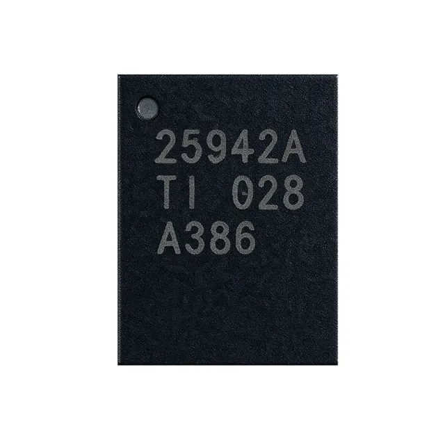
TPS25940ARVCR - 18V 5A eFuse with True Reverse Blocking | TI
The Texas Instruments TPS25940ARVCR is a 2.7V to 18V, 42mΩ, 0.6A to 5.2A electronic fuse (eFuse) with true reverse-current blocking and DevSleep support, housed in a 20-pin WQFN (RVC) 4x3 mm package. The device integrates a low-Rdson N-channel FET, programmable current limit, and load-protection features, targeting SSD, USB Type-C, and hot-swap power paths. The 5.3A maximum load current and 42mΩ on-resistance minimize power dissipation during steady-state operation. Reverse-current blocking prevents current backflow when the output voltage exceeds the input, a critical feature for systems with multiple parallel power sources or battery-backed rails. DevSleep support enables very-low quiescent current in deep-sleep states, an essential characteristic for SSD power-management ICs and battery-powered portable equipment. An eFuse (electronic fuse) is a semiconductor protection device that combines the function of a traditional fuse, current-limiting circuit, and load switch into a single integrated circuit. It sits between a power source and a downstream load to provide inrush current limiting, overcurrent protection, short-circuit protection, reverse-current blocking, and often overvoltage/undervoltage protection. Unlike a one-time-use fuse, an eFuse can be reset by toggling its enable input. In the broader system hierarchy, an eFuse is a subcategory of hot-swap controller / power-distribution switch, which itself falls under power management IC and finally semiconductor device. Key features include 2.7V to 18V operating input range, 0.6A to 5.2A programmable current limit (set via external resistor), ±8% ILIM accuracy over temperature, integrated true reverse-current blocking, programmable inrush current slew rate via dVdt pin, fault output (FLT) pin for system monitoring, thermal shutdown, and an EN/UVLO pin for precise turn-on control. The device supports the SATA DevSleep specification, drawing microamp-level quiescent current during sleep to meet SSD power budgets. The TPS25940 family uses a charge-pump-driven N-channel MOSFET architecture with an integrated gate driver. The true reverse-current block comparator monitors VOUT versus VIN and disables the FET when VOUT > VIN, preventing discharge of downstream capacitance into the input rail. The DEVSLP pin activates a low-quiescent-current mode by disabling most internal circuits while keeping reverse-blocking monitoring active. The device operates from -40C to +85C ambient. Typical applications include NVMe/SATA SSD power rails, USB Type-C VBUS hot-swap protection, multi-port USB hubs, fan protection circuits, and any 5V/12V rail that requires inrush control and disconnect on fault. When designing with this eFuse, place the ILIM resistor close to the ILIM pin to minimize noise pickup, use a 1µF or larger input bulk capacitor to suppress voltage transients during hot-plug events, and observe absolute maximum VIN of 20V including transient ringing. The package's thermal pad must be soldered to a sufficiently large copper pour to handle steady-state I²R dissipation - at 5A continuous through 42mΩ, the part dissipates ~1.05W. This page synthesizes distributor pricing, drop-in alternatives, and practical design notes not found on the manufacturer product page.
TPS259470ARPWR - 5.5A eFuse w/ Reverse Polarity Protection | TI
The Texas Instruments TPS259470ARPWR is a 5.5 A, 28 mΩ true reverse-current-blocking electronic fuse (eFuse) with integrated input reverse polarity protection, housed in a 10-pin VQFN-HR (RPW) 2x2 mm package. It operates from 2.7 V to 23 V input and is characterized for junction temperatures from -40 °C to +125 °C. The device integrates a low-impedance N-channel MOSFET, programmable current limit, overvoltage lockout, and fast fault response to protect downstream loads from inrush, short circuit, and incorrect adapter polarity events. An electronic fuse (eFuse) is a solid-state power switch and protection IC that replaces traditional PTC fuses, Schottky OR-ing diodes, and discrete hot-swap circuits. It sits between a system input rail and downstream converters, providing controlled turn-on, accurate current limiting, and fast interruption on fault. The TPS259470 in particular is part of TI's hot-swap/eFuse family that combines input reverse polarity protection, true reverse-current blocking (does not rely on body diode conduction), programmable overvoltage, and fault output signaling in one IC. Key specifications include a 28 mΩ typical on-resistance, 5.5 A continuous load current capability, adjustable overvoltage lockout, active current limit with auto-retry response, and an open-drain fault indicator (FLT). The integrated reverse polarity protection eliminates the need for a series input Schottky diode, reducing conduction loss by typically 30-60% versus traditional reverse-polarity Schottky solutions, while true reverse-current blocking prevents back-feeding when a higher-voltage adapter is hot-plugged in parallel with a lower-voltage source. Architecturally, the TPS259470 uses an internal N-channel MOSFET with a charge-pump gate driver, a precision current-sense amplifier, and a fault state machine. The 2.7 V UVLO ensures clean startup in low-voltage USB-PD and industrial 5 V/12 V/19 V/20 V rails. Because the IC is characterized for -40 °C to +125 °C junction and is available in a thermally enhanced VQFN-HR 2x2 mm package, it is suitable for compact, high-ambient-temperature applications where PCB area is at a premium. Typical applications include USB Type-C / USB-PD source and sink protection, multi-port USB hubs, industrial PLC and sensor power rails, telecom router line cards, and battery backup systems. The device is especially useful wherever an adapter, battery, or USB-PD source must be hot-plugged into a live system without causing inrush latch-up or back-power through the input. When designing in, keep input/output traces short and use low-ESR ceramic bypass capacitance close to VIN and PGND. The TIMER capacitor sets the fault retry interval and must be sized for the actual upstream supply ramp rate. Always cross-check thermal dissipation versus continuous load to avoid triggering thermal shutdown in enclosed adapters. This page distills datasheet values, drop-in alternatives, and design notes not available on the manufacturer summary page to help engineers select and implement the part quickly.

TPS26633PWPR - 60V 6A eFuse HTSSOP-20 | Texas Instruments
The Texas Instruments TPS26633PWPR is a 4.5V to 60V, 31mΩ, 0.6A to 6A industrial eFuse with output power limiting and surge protection, housed in a 20-pin HTSSOP (PWP) package with exposed thermal pad. It integrates a 60V hot-swap FET, supports reverse polarity protection with an external N-channel FET, and delivers ±7% accurate adjustable current limit. Absolute maximum input voltage is rated at 67V, allowing robust transient tolerance on industrial 24V and 48V buses. An eFuse (electronic fuse) is a semiconductor-based circuit protection device that replaces traditional mechanical fuses, PTCs, and discrete hot-swap circuits. It combines a power MOSFET, current-sense amplifier, and control logic in one IC, sitting in the power management hierarchy between discrete MOSFETs and full system PMICs. Compared with a PTC or polyfuse, an eFuse offers precise, programmable current limit, fast fault response, and automatic retry, and it does not require physical replacement after a trip event. Key features of the TPS26633PWPR include 4.5V to 60V operating range, integrated 31mΩ RON hot-swap FET, 0.6A to 6A adjustable current limit with ±7% accuracy, output power limiting for surge compliance, reverse current blocking, fault output indicator, and thermal shutdown. The HTSSOP-20 PowerPAD package provides a low thermal resistance path for sustained 6A operation, and the device operates from -40C to +125C junction temperature. The device uses TI's hot-swap controller architecture with charge-pump gate drive and precision current sensing, providing monotonic dV/dt controlled startup to limit inrush current. The output power-limit feature clamps transient power to a programmed threshold for IEC 61000-4-5 surge compliance, while the timer-based fault response prevents nuisance tripping on capacitive loads. Typical applications include industrial PLC I/O protection, 24V factory automation power rails, motor-drive auxiliary supplies, building-automation controllers, and telecom 48V line-card protection. The wide input range makes it well suited for systems powered from 24V industrial buses or 48V PoE/PoE+ sources where input transients and reverse-wiring events are common. When designing with the TPS26633PWPR, place input and output bulk capacitors close to the IC, connect the PowerPAD to a 1-square-inch copper pour, and program the current limit with a 1% resistor to achieve the ±7% accuracy. Always verify SOA under worst-case VIN and I²t conditions in the datasheet. This page synthesizes distributor pricing, drop-in HTSSOP-20 alternatives, and practical design notes not found in the manufacturer datasheet.